SC05-11EWA中文资料
2N5551中文资料(fairchild)中文数据手册「EasyDatasheet - 矽搜」
50 VCB = 100V
10
10
10
1β
100 Co
o
125 C
0.1
o
-40 Co
25 Co
75 C
- CCEO(SALT)LECTOR-EMITTER VOLTAGE [V]
0.01
V
1
10
100
IC- COLLECTOR CURRENT [mA]
Figure 2. Collector-Emitter Saturation Voltage vs.
芯片中文手册,看全文,戳
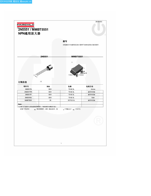
2N5551 / MMBT5551 NPN通用放大器
2013年6月
描写
该装置是专为通用高压放大器和气体放电的显示驱动程序.
2N5551
TO-92
MMBT5551
3
2
1 SOT-23
Marking: 3S 1. Base 2. Emitter 3. Collector
MMBT5551
350 2.8
357
Units
mW mW/°C °C/W °C/W
2
芯片中文手册,看全文,戳
电气特性
(4)
价值观是在T 符
A = 25°C除非另有说明. 参数
断特性
V(BR)CEO 集电极 - 发射极击穿电压 V(BR)CBO 集电极基击穿电压 V (BR)EBO 发射极基极击穿电压
Value
160 180
6 600 -55到+150
2N5551 / MMBT5551 - NPN通用放大
器
Units
V V V mA °C
热特性
价值观是在T
EE-SPX304-W2A中文资料(omron)中文数据手册「EasyDatasheet - 矽搜」
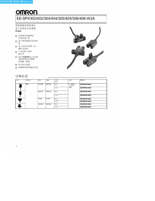
Extension cable
避免从微型光电断开时电源被提供给微型光电或微型光电可
能会损坏.
如果金属安装基座进行感性电
噪音,可微型光电被意外激活.如果 噪音是个问题,采取以下预防措施:
1. GND端子连接到安装基座,于是就有 是在微型光电和安装基座之间电势没有差别.
2.通过GND端子连接到安装基座
0.47- µF电容.
间距d(毫米)
在TR上
Dark-ON mode
在TR上
Dark-ON mode
EE-SPX305-W2 d A
d
注:EE-SPX405-W2A检测位置特性是相反那
些EE-SPX305-W2A.
TR关闭
间距d(毫米)
TR关闭
间距d(毫米)
操作
J 内部/外部接线图
光时 ON /遮光时 ON
Operation indicator
零件号
EE-SPX302-W2A EE-SPX402-W2A EE-SPX304-W2A EE-SPX404-W2A EE-SPX305-W2A EE-SPX405-W2A EE-SPX306-W2A EE-SPX406-W2A
1
芯片中文手册,看全文,戳
EE- -SPX302/402/304/404/305/405/306/406- -W2A
20 (0.79)
6.95(0.27)
14.5 (0.57)
1000±30
端子配置
红色(褐色)V CC
白色(黑色)输出
黑(蓝色)GND(0V)
IEC colors are shown in parentheses.
4
芯片中文手册,看全文,戳
EE- -SPX302/402/304/404/305/405/306/406- -W2A
SMS05C中文资料
110 100
90 80 70 60 50 40 30 20 10
0 0
25
50
75
100
125
150
Ambient Temperature - TA (oC)
Clamping Voltage vs. Peak Pulse Current
Clamping Voltage - VC (V)
45
40 SMS24C
Non-Repetitive Peak Pulse Power vs. Pulse Time
10
Peak Pulse Power - PPP (kW)
1
0.1
Percent of IPP
0.01 0.1
110 100
90 80 70 60 50 40 30 20 10
0 0
1
10
100
Pulse Duration - tp (µs)
SMS15C Parameter
Reverse Stand-Off Voltage Reverse Breakdown Voltage Reverse Leakage Current Clamping Voltage Clamping Voltage Junction Capacitance
Symbol VRWM VBR IR VC VC Cj
Minimum
It = 1mA
6
VRWM = 5V, T=25°C
IPP = 5A, tp = 8/20µs
IPP = 24A, tp = 8/20µs
Between I/O Pins and Gnd
VR = 0V, f = 1MHz
Typical 325
SC111中文资料

PRELIMINARY - October 9, 2000TEL:805-498-2111 FAX:805-498-3804 WEB:PRELIMINARY - October 9, 2000ELECTRICAL CHARACTERISTICSUnless specified: V CC = 4.75V to 12.6V; GND = PGND = 0V; FB = V O ; V BSTL = 12V; V BSTH-PHASE = 12V; T J = 25o C PARAMETER CONDITIONSMINTYPMAXUNITSPOWER SUPPLY Supply Voltage V CC 4.412.6V Supply Current EN = V CC8mA Line RegulationV IN = 2.5 ± 0.5V, V O = V IN /2 @ 0A0.5%UNDER VOLTAGE LOCKOUT Turn-On Threshold TBD 4.2TBD V Turn-Off Threshold TBD4.0TBDVERROR AMPLIFIER Transconductance 2mS Open Loop DC Gain 50dB Bandwidth -3dB 500kHz COMP Source Capability ±250µA Input Bias 58µAOSCILLATOR Oscillator Frequency 225250275kHz Oscillator Max Duty Cycle 9095%Ramp Height 1VTIMINGMinimum Off-Time 100ns Dead Time80nsABSOLUTE MAXIMUM RATINGSParameter Symbol Maximum Units V CC , BSTL to GND V IN-0.5 to 14V PGND to GND ± 0.5V PHASE to GND -0.5 to 18V BSTH to PHASE14V Thermal Resistance Junction to Case θJC 45°C/W Thermal Resistance Junction to Ambient θJA 115°C/W Operating Temperature Range T A 0 to 70°C Storage Temperature Range T STG -65 to +150°C Lead Temperature (Soldering) 10 secT LEAD 300°CPRELIMINARY - October 9, 2000BLOCK DIAGRAMELECTRICAL CHARACTERISTICSUnless specified: V CC = 4.75V to 12.6V; GND = PGND = 0V; FB = V O ; V BSTL = 12V; V BSTH-PHASE = 12V; T J = 25o C PARAMETER CONDITIONS MIN TYP MAX UNITS MOSFET DRIVERSPeak DH Sink/Source Current BSTH - DH = 4.5V, DH - PHASE = 3.0V0.5A DH - PHASE = 1.5V0.1Peak DL Sink/Source CurrentBSTL - DL = 4.5V, DL - GND = 3.0V0.5ADL - GND = 1.5V0.1PROTECTIONOver Current Set Isource V OCSET = 4.5V 180200220µA SOFT START Charge Current V SS = 1.5V 10µA Discharge Current V SS = 1.5V2µA POWER GOOD Upper Threshold 112%Lower Threshold 88%PWRGD Voltage Low I PWRGD = 2mA0.5V REFERENCEREFOUT Source Current 3mAInput Bias58µANOTE:(1) Specification refers to application circuit (Figure 1.).PIN DESCRIPTIONPin #Pin Name Pin Function1 VCC Chip supply voltage.2SS/ENBL Soft start/Enable.3OCSET Current limit set point.4PWRGD Logic high indicates correct output.5GND Ground.6PHASE Phase node connection between MOSFET’s.7DL Low side driver output.8DH High side driver output.9BSTH High side drive supply.10BSTL Low side drive supply.11COMP Error amplifier output, compensation.12SENSE Error amplifier negative input.13REFIN Error amplifier positive input.14REFOUT Buffered reference voltage.NOTE:(1) All logic level inputs and outputs are open collector TTL compatible.PRELIMINARY - October 9, 2000THEORY OF OPERATIONSynchronous Buck ConverterV TERMINATION power is provided by a synchronous,voltage-mode pulse width modulated (PWM) controller.This section has all the features required to build a high efficiency synchronous buck converter for termi-nation of power application.The output voltage of the synchronous converter is set and controlled by the output of the error amplifier. The resistive divider generates reference voltage for the error amplifier from an external chipset voltage which is usually 2.5V. The inverting input of the error amplifier receives its voltage from the SENSE pin.The internal oscillator uses an on-chip capacitor and trimmed precision current sources to set the oscillation frequency to 250kHz. The triangular output of the os-cillator sets the reference voltage at the inverting input of the PWM comparator. The non-inverting input of the comparator receives it’s input voltage from the error amplifier. When the oscillator output voltage drops be-low the error amplifier output voltage, the comparator output goes high. This pulls DL low, turning off the low-side FET, and DH is pulled high, turning on the high-side FET (once the cross-current control allows it).When the oscillator voltage rises back above the error amplifier output voltage, the comparator output goes low. This pulls DH low, turning off the high-side FET,and DL is pulled high, turning on the low-side FET (once the cross-current control allows it).As SENSE increases, the output voltage of the error amplifier decreases. This causes a reduction in the on-time of the high-side MOSFET connected to DH,hence lowering the output voltage.Under Voltage LockoutThe under voltage lockout circuit of the SC1110 as-sures that both the high-side MOSFET driver outputs remain in the off state whenever the supply voltage drops below set parameters. Lockout occurs if V CC falls below 4.0V. Normal operation resumes once V CC rises above 4.2V.Soft StartInitially, SS/ENABLE sources 10µA of current tocharge an external capacitor. The outputs of the error amplifiers are clamped to a voltage proportional to the voltage on SS/ENABLE. This limits the on-time of the high-side MOSFETs, thus leading to a controlled ramp-up of the output voltages.R DS(ON) Current LimitingThe current limit threshold is set by connecting an ex-ternal resistor from the V CC supply to OCSET. The volt-age drop across this resistor is due to the 200µA inter-nal sink sets the voltage at the pin. This voltage is compared to the voltage at the PHASE node. This comparison is made only when the high-side drive is high to avoid false current limit triggering due to uncon-tributing measurements from the MOSFET’s off-voltage. When the voltage at PHASE is less than the voltage at OCSET, an overcurrent condition occurs and the soft start cycle is initiated. The synchronous switcher turns off and SS/ENABLE starts to sink 2µA.When SS/ENABLE reaches 0.8V, it then starts to source 10µA and a new cycle begins.Hiccup ModeDuring power up, the SS/ENABLE pin is internally pulled low until VCC reaches the undervoltage lockout level of 4.2V. Once V CC has reached 4.2V, the SS/EN-ABLE pin is released and begins to source 10µA of current to the external soft-start capacitor. As the soft-start voltage rises, the output of the internal error am-plifier is clamped to this voltage. When the error signal reaches the level of the internal triangular oscillator,which swings from 1V to 2V at a fixed frequency of 250kHz, switching occurs. As the error signal crosses over the oscillator signal, the duty cycle of the PWM signal continues to increase until the output comes into regulation. If an over-current condition has not oc-curred the soft-start voltage will continue to rise and level off at about 2.2V.An over-current condition occurs when the high-side drive is turned on, but the PHASE node does not reach the voltage level set at the OCSET pin. ThePHASE node is sampled only once per cycle during the valley of the triangular oscillator. Once an over-current occurs, both the high-side and low-side drivers turn off and the SS/ENABLE pin begins to sink 2uA. The soft-start voltage will begin to decrease as the 2uA of cur-rent discharges the external capacitor. When the soft-start voltage reaches 0.8V, the SS/ENABLE pin will be-gin to source 10uA and begin to charge the external capacitor causing the soft-start voltage to rise again.Again, when the soft-start voltage reaches the level of the internal oscillator, switching will occur.If the over-current condition is no longer present, nor-mal operation will continue. If the over-current condi-tion is still present, the SS/ENABLE pin will again begin to sink 2uA. This cycle will continue indefinitely until the over-current condition is removed.PRELIMINARY - October 9, 2000 SIMULATION WAVEFORMS 2.5V and 1.25V ramp upOutput current of the VTT supplyPRELIMINARY - October 9, 2000 OUTLINE DRAWING SO-14ECN00-1363。
反射光电ex-11ea手册

反射光电EX-11EA手册提供了该型号传感器的详细信息和使用指南。
EX-11EA是一种超薄型光电传感器,内置放大器,适用于各种检测应用,如印刷电路板定位、IC检测等。
它具有以下特点:
1. 符合标准:该型号符合EMC指令EN60947-5-2、RoHS指令以及ISO13849-1(1类,PLc)标准。
2. 检测能力:EX-11EA能够检测最小直径为1mm的不透明物体,检测距离可达150mm。
3. 安装方式:它设计有安装孔,方便用户根据需要安装在不同的位置上。
传感器由投光部和受光部组成,工作时会有指示灯显示其工作状态。
4. 平行移动特性:透过型的EX-11E和EX-15E型号在平行移动时具有特定的特性,例如在一定的位移范围内保持检测稳定性。
5. 应用场景:EX-11EA-PN型号适用于多种应用场景,包括印刷电路板定位、IC检测、印刷电路板机架检测、晶片盒检测、薄环检测以及检查托盘中是否存在电容器等。
PSC05-11EWA, 规格书,Datasheet 资料
High Efficiency Red 75 30 160 5 -40°C To +85°C 260°C For 3-5 Seconds
Units mW mA mA V
Note: 1. Luminous intensity/ luminous Flux: +/-15%.
Electrical / Optical Characteristics at TA=25°C
Symbol λpeak λD [1] Δλ1/2 C VF [2] IR Parameter Peak Wavelength Dominant Wavelength Spectral Line Half-width Capacitance Forward Voltage Reverse Current Device High Efficiency Red High Efficiency Red High Efficiency Red High Efficiency Red High Efficiency Red High Efficiency Red Typ. 627 625 45 15 2.0 2.5 10 Max. Units nm nm nm pF V uA Test Conditions IF=20mA IF=20mA IF=20mA VF=0V;f=1MHz IF=20mA VR=5V
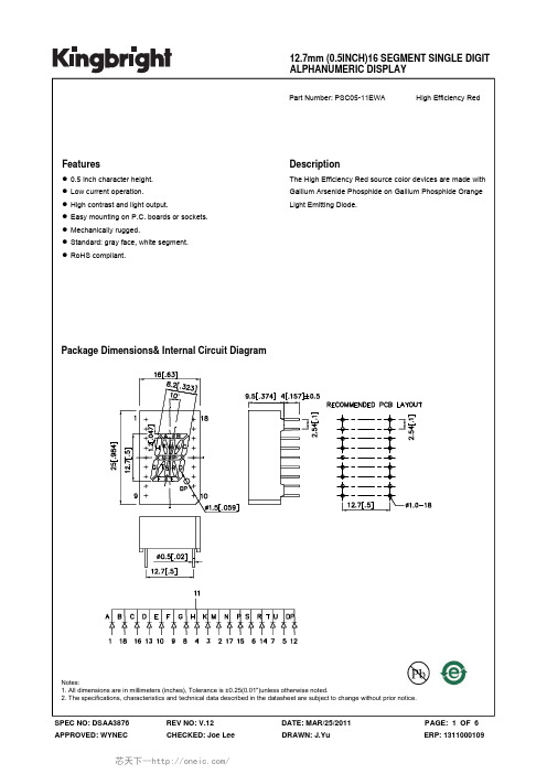
12.7mm (0.5INCH)16 SEGMENT SINGLE DIGIT ALPHANUMERIC DISPLAY
Part Number: PSC05-11EWA High Efficiency Red
SC1105CS.TR中文资料
POWER MANAGEMENTSC1105/6Voltage ModePWM ControllerPRELIMINARY FeaturesApplicationsDescriptionThe SC1105 is an asynchronous voltage mode PWM controller for applications that require an option of two voltages. An input is provided to select either the input voltage (VIN) or a user programmed voltage at the output.When the PWM is enabled the 200kHz fixed frequency PWM regulates the output to either a fixed voltage of 1.5V (SC1105) or a user programmed voltage (SC1106). When the PWM is disabled the high side MOSFET gate is turned on to deliver the input voltage directly to the output.The SC1105/6 internal architecture and functional blocks are based on the SC1101 integrated circuit, therefore, the layout guidelines and reference circuits can be readily applied.u Low cost / small sizeu Switch mode efficiency > 85%u1% reference voltage accuracyu500mA output driveu SO-8 packageu Switchable AGP supply 1.5V or 3.3Vu Peripheral card supplies (backward compatibility) u User selectable edge connectorsu PCMCIA cardsPOWER MANAGEMENT PRELIMINARYElectrical CharacteristicsAbsolute Maximum Ratingsr e t e m a r a P l o b m y S m u m i x a M s t i n U e g a t l o V t u p n I V C C D N G o t 7+o t 3.0-V l a i t n e r e f f i D d n u o r G P D N G D N G o t +1V e g a t l o V t u p n I t s o o B DN G o t T S B 51+o t 3.0-V e r u t a r e p m e T g n i t a r e p O T A 07+o t 0C °eg n a R e r u t a r e p m e T e g a r o t S T G T S 521+o t 54-C °.c e S 01)g n i r e d l o S (e r u t a r e p m e T d a e L T L 003C °t n e i b m A o t n o i t c n u J ,e c n a t s i s e R l a m r e h T q A J 561W /C °e s a C o t n o i t c n u J ,e c n a t s i s e R l a m r e h T q C J 04W /C °)l e d o M y d o B n a m u H (g n i t a R D S E DS E 2Vk V CC = 4.75V to 5.25V; GND = P GND = 0V; V O = 1.5V; T A = 25°C; BST = 12V; 2A; V IN = 3.3V + 5%.Per test circuit, unless otherwise specified.r e t e m a r a P l o b m y S s n o i t i d n o C n i M p y T x a M s t i n U ec n e r e f e R V FE R 832.1052.1362.1Vpm e T r e v O 522.1052.1572.1t n e r r u C s a i B E S N E S O V I B 6011C S 0.20.8A µt n e r r u C t n e c s e i u Q I Q V o t n i t n e r r u C C C n i p 0.50.8A m d a o L n o i t a l u g e R G E R D A O L I O A8o t A 1=5.00.1%e n i L n o i t a l u g e R G E R E N I L 1.0%y c n e u q e r F r o t a l l i c s O C S O 081002022z H k e l c y C y t u D x a M .c .d 0959%tn e r r u C e c r u o S /k n i S H D I OV T S B V 5.4=H D -V (H D V -D N G P )V 2=005AmPOWER MANAGEMENT PRELIMINARY Test CircuitPOWER MANAGEMENT PRELIMINARYBlock DiagramPin ConfigurationOrdering InformationPin DescriptionsTop View(8 Lead Plastic SOIC)ec i v e D )1(e g a k c a P T (e g n a R p m e T J )R T .S C 5011C S 8-O S C °521o t °0RT .S C 6011C S 8-O S C°521o t °0Note:(1) Only available in tape and reel packaging. A reel contains 2500 devices.#n i P em a N n i P no i t c n u F n i P 1V C C .e g a t l o v y l p p u s e c i v e D 2C N .n o i t c e n n o c o N 3#T E D E P Y T .e l b i t a p m o c L T T -t u p n i l e v e l c i g o L .V 5.1=o L ;V 3.3=i H ,t c e l e s e g a t l o v t u p t u O 4D N G P .d n u o r g r e w o p e c i v e D 5H D .t u p t u o r e v i r d e d i s h g i H 6T S B .r e v i r d e d i s h g i h r o f y l p p u S V 217E S N E S O V .n i a h c k c a b d e e f l a n r e t n i f o d n e p o T 8DN G .d n u o r g l a n g i s l l a m SPOWER MANAGEMENT PRELIMINARY Typical CharacteristicsPOWER MANAGEMENT PRELIMINARYSemtech CorporationPower Management Products Division 652 Mitchell Rd., Newbury Park, CA 91320Phone: (805)498-2111 FAX (805)498-3804Outline DrawingContact InformationLand Pattern - SO-8。
CS-iTWD-05 无线水浸智能监测终端 使用说明书

CS-iTWD-05 无线水浸智能监测终端使用说明书(CS-iTWD-05-SS)(REV:A)西安中星测控有限公司修订履历修订日期版本修订内容修订人2019/04/22 A 首次发布晏峰编制审核标准化批准签名日期注:本签署页仅限公司内部使用。
目次1 概述 (1)1.1 产品简介 (1)1.2 工作原理 (1)2 技术指标 (2)2.1 主要技术参数 (2)2.2 外形尺寸 (2)3 使用说明 (3)3.1 安装SIM卡 (3)3.2 安装电池 (3)3.3 入网说明 (4)3.4 通信协议 (4)4 安装方法 (4)5 选型指导 (6)6 附件 (7)7 注意事项 (7)7.1 终端联网不成功 (7)7.2 产品可能因以下原因产生漏报现象 (7)8 声明 (7)CS-iTWD-05无线水浸智能监测终端使用说明书1 概述1.1 产品简介无线水浸智能监测终端用于监测是否有水浸入,当有水浸入时会触发终端报警,报警信号通过无线传输方式发送至监控中心,监控中心对数据进行解析并判断警情。
该终端产品提供LoRaWAN、NBIOT、GPRS三种无线通讯方式,可应用于路基浸水、机房浸水、桥下积水等应用场合的监测。
终端产品使用电池供电,具有安装方便、电池寿命长、检测准确率高,工作稳定等特点。
图1 无线水浸智能监测终端示意图1.2 工作原理无线水浸智能监测终端采用漏水探测电极进行水浸探测,当探头的两个电极被水浸入时,触发终端报警并通过无线网络将报警信息发送至监控中心。
2 技术指标2.1 主要技术参数无线水浸智能监测终端的主要技术指标见表1所示。
表1 主要技术参数名称技术参数备注工作频段434MHz/470MHz/868MHz/915MHz LoRaWAN B1/B3/B5/B8/B20 NB-IoT 850/900/1800/1900MHz GPRS设备类型Class A LoRaWAN天线接口FPC天线工作电压锂电池供电ER26500(3.6V)ER26500+SPC1550电池寿命3-5年工作正常且每天最多两次上报数据工作最大电流<200mA LoRaWAN <350mA NB-IoT <2000mA GPRS休眠电流<25.0μA线缆长度3米(默认)长度可定制防护等级IP68外壳材质采用PC+ABS防老化、防腐蚀,防撞击材料工作温度(-25~+85)℃消费级SIM卡(-40~+85)℃工业级SIM卡/ LoRaWAN 存储温度(-40~+85)℃2.2 外形尺寸无线水浸智能监测终端的外形及尺寸标注见图2所示。
- 1、下载文档前请自行甄别文档内容的完整性,平台不提供额外的编辑、内容补充、找答案等附加服务。
- 2、"仅部分预览"的文档,不可在线预览部分如存在完整性等问题,可反馈申请退款(可完整预览的文档不适用该条件!)。
- 3、如文档侵犯您的权益,请联系客服反馈,我们会尽快为您处理(人工客服工作时间:9:00-18:30)。
Package Dimensions & Internal Circuit Diagram
Notes: 1. All dimensions are in millimeters (inches), Tolerance is ±0.25(0.01")unless otherwise noted. 2. Specifications are subject to change whitout notice.
元器件交易网
12.7mm (0.5INCH) SINGLE DIGIT NUMERIC DISPLAYS
SA05-11EWA/GWA/YWA/SRWA SC05-11EWA/GWA/YWA/SRWA
Features
0.5 INCH DIGIT HEIGHT. LOW CURRENT OPERATION. EXCELLENT CHARACTER APPEARANCE. EASY MOUNTING ON P.C. BOARDS OR SOCKETS. I.C. COMPATIBLE. CATEGORIZED FOR LUMINOUS INTENSITY, YELLOW AND GREEN CATEGORIZED FOR COLOR. MECHANICALLY RUGGED. STANDARD : GRAY FACE, WHITE SEGMENT.
Description
The High Efficiency Red source color devices are made with Gallium Arsenide Phosphide on Gallium Phosphide Orange Light Emitting Diode. The Green source color devices are made with Gallium Phosphide Green Light Emitting Diode. The Yellow source color devices are made with Gallium Arsenide Phosphide on Gallium Phosphide Yellow Light Emitting Diode. The Super Bright Red source color devices are made with Gallium Aluminum Arsenide Red Light Emitting Diode.
Electrical / Optical Characteristics at T)=25°C °
Sy m b o l Par am et er D ev i c e High Efficiency Red Green Yellow Super Bright Red High Efficiency Red Green Yellow Super Bright Red Ty p . 627 565 590 660 625 568 588 640 45 30 35 20 15 15 20 45 2.0 2.2 2.1 1.85 2.5 2.5 2.5 2.5 10 Max . Un it s Tes t Co n d it io n s
nm
IF=20mA
C
pF
VF=0V;f=1MHz
VF IR
Forward Voltage
V
IF=20mA
Reverse Current
uA
V R = 5V
SPEC NO: CDA0851 APPROVED:J.LU
REV NO: V.1 CHECKED:
DATE: NOV/18/2001 DRAWN: S.H.CHEN
Super Bright Red
SPEC NO: CDA0851 APPROVED:J.LU
REV NO: V.1 CHECKED:
DATE: NOV/18/2001 DRAWN: S.H.CHEN
PAGE: 5 OF 5
PAGE: 2 OF 5
元器件交易网
Absolute Maximum Ratings at T)=25°C °
Par am et er Power dissipation DC Forward Current Peak Forward Current [1] Reverse Voltage Operating/Storage Temperature Lead Solder Temperature [2]
S u p er B r i g h t R ed 100 30 15 5 5
Un it s mW mA mA V
High Efficiency Red
SPEC NO: CDA0851 APPROVED:J.LU
REV NO: V.1 CHECKED:
DATE: NOV/18/2001 DRAWN: S.H.CHEN
SPEC NO: CDA0851 APPROVED:J.LU
REV NO: V.1 CHECKED:
DATE: NOV/18/2001 DRAWN: S.H.CHEN
PAGE: 1 OF 5
元器件交易网
Selection Guide
Par t No . SA05-11EWA SC05-11EWA SA05-11GWA SC05-11GWA SA05-11YWA SC05-11YWA SA05-11SRWA SC05-11SRWA SUPER BRIGHT RED (GaAlAs) 8000 24000 YELLOW (GaAsP/GaP) 1900 4700 GREEN (GaP) 3000 10500 HIGH EFFICIENCY RED (GaAsP/GaP) 3 0 00 800 0 Dic e Iv (u c d ) @ 10 m A Min . Ty p .
λpeak
Peak Wavelength
nm
IF=20mA
λD
Dominate Wavelength
nm
IF=20mA
∆λ1/2
High Efficiency Red Spectral Line Halfwidth Green Yellow Super Bright Red Capacitance High Efficiency Red Green Yellow Super Bright Red High Efficiency Red Green Yellow Super Bright Red All
Notes: 1. 1/10 Duty Cycle, 0.1ms Pulse Width. 2. 4mm below package base.
H i g h E f f i c i en c y R ed 105 30 160 5
Gr een 105 25 140 5
Yello w 10 5 30 140 5 -40°C To +85°C 260°C For 5 Seconds
D es c r i p t i o n Common Anode, Rt Hand Decimal Common Cathode, Rt. Hand Decimal Common Anode, Rt Hand Decimal Common Cathode, Rt. Hand Decimal Common Anode, Rt Hand Decimal Common Cathode, Rt. Hand Decimal Common Anode, Rt Hand Decimal Common Cathode, Rt. Hand Decimal
PAGE: 3 OF 5
元器件交易网
Green
Yellow
SPEC NO: CDA0851 APPROVED:J.LU
REV NO: V.1 CHECKED:
DATE: NOV/18/2001 DRAWN: S.H.CHEN
PAGE