MAX5923EUP+;MAX5923EUP+T;中文规格书,Datasheet资料
APL5912中文资料

C1 (pF) 27 36 68
Absolute Maximum Ratings
Symbol VCNTL VIN VI/O VPOK PD PPEAK TJ TSTG TSDR VESD Parameter VCNTL Supply Voltage (VCNTL to GND) VIN Supply Voltage (VIN to GND) EN and FB to GND POK to GND Average Power Dissipation Peak Power Dissipation (<20mS) Junction Temperature Storage Temperature Soldering Temperature, 10 Seconds Minimum ESD Rating (Human Body Mode) Rating -0.3 ~ 7 -0.3 ~ 3.3 -0.3 ~ VCNTL+0.3 -0.3 ~ 7 3 20 150 -65 ~ 150 300 ±2 Unit V V V V W W
APL5912 KA :
APL5912 XXXXX
Note: ANPEC lead-free products contain molding compounds/die attach materials and 100% matte tin plate termination finish; which are fully compliant with RoHS and compatible with both SnPb and lead-free soldiering operations. ANPEC lead-free products meet or exceed the lead-free requirements of IPC/JEDEC J STD-020C for MSL classification at lead-free peak reflow temperature.
MAX13085EESA-T中文资料

General DescriptionThe MAX13080E–MAX13089E +5.0V, ±15kV ESD-protect-ed, RS-485/RS-422 transceivers feature one driver and one receiver. These devices include fail-safe circuitry,guaranteeing a logic-high receiver output when receiver inputs are open or shorted. The receiver outputs a logic-high if all transmitters on a terminated bus are disabled (high impedance). The MAX13080E–MAX13089E include a hot-swap capability to eliminate false transitions on the bus during power-up or hot insertion.The MAX13080E/MAX13081E/MAX13082E feature reduced slew-rate drivers that minimize EMI and reduce reflections caused by improperly terminated cables, allowing error-free data transmission up to 250kbps. The MAX13083E/MAX13084E/MAX13085E also feature slew-rate-limited drivers but allow transmit speeds up to 500kbps. The MAX13086E/MAX13087E/MAX13088E driver slew rates are not limited, making transmit speeds up to 16Mbps possible. The MAX13089E slew rate is pin selectable for 250kbps,500kbps, and 16Mbps.The MAX13082E/MAX13085E/MAX13088E are intended for half-duplex communications, and the MAX13080E/MAX13081E/MAX13083E/MAX13084E/MAX13086E/MAX13087E are intended for full-duplex communica-tions. The MAX13089E is selectable for half-duplex or full-duplex operation. It also features independently programmable receiver and transmitter output phase through separate pins.The MAX13080E–MAX13089E transceivers draw 1.2mA of supply current when unloaded or when fully loaded with the drivers disabled. All devices have a 1/8-unit load receiver input impedance, allowing up to 256transceivers on the bus.The MAX13080E/MAX13083E/MAX13086E/MAX13089E are available in 14-pin PDIP and 14-pin SO packages.The MAX13081E/MAX13082E/MAX13084E/MAX13085E/MAX13087E/MAX13088E are available in 8-pin PDIP and 8-pin SO packages. The devices operate over the com-mercial, extended, and automotive temperature ranges.ApplicationsUtility Meters Lighting Systems Industrial Control Telecom Security Systems Instrumentation ProfibusFeatures♦+5.0V Operation♦Extended ESD Protection for RS-485/RS-422 I/O Pins±15kV Human Body Model ♦True Fail-Safe Receiver While Maintaining EIA/TIA-485 Compatibility ♦Hot-Swap Input Structures on DE and RE ♦Enhanced Slew-Rate Limiting Facilitates Error-Free Data Transmission(MAX13080E–MAX13085E/MAX13089E)♦Low-Current Shutdown Mode (Except MAX13081E/MAX13084E/MAX13087E)♦Pin-Selectable Full-/Half-Duplex Operation (MAX13089E)♦Phase Controls to Correct for Twisted-Pair Reversal (MAX13089E)♦Allow Up to 256 Transceivers on the Bus ♦Available in Industry-Standard 8-Pin SO PackageMAX13080E–MAX13089E+5.0V , ±15kV ESD-Protected, Fail-Safe, Hot-Swap, RS-485/RS-422 Transceivers________________________________________________________________Maxim Integrated Products 1Ordering Information19-3590; Rev 1; 4/05For pricing, delivery, and ordering information,please contact Maxim/Dallas Direct!at 1-888-629-4642, or visit Maxim’s website at .Selector Guide, Pin Configurations, and Typical Operating Circuits appear at end of data sheet.Ordering Information continued at end of data sheet.M A X 13080E –M A X 13089E+5.0V , ±15kV ESD-Protected, Fail-Safe, Hot-Swap, RS-485/RS-422 Transceivers 2_______________________________________________________________________________________ABSOLUTE MAXIMUM RATINGSDC ELECTRICAL CHARACTERISTICS(V CC = +5.0V ±10%, T A = T MIN to T MAX , unless otherwise noted. Typical values are at V CC = +5.0V and T A = +25°C.) (Note 1)Stresses beyond those listed under “Absolute Maximum Ratings” may cause permanent damage to the device. These are stress ratings only, and functional operation of the device at these or any other conditions beyond those indicated in the operational sections of the specifications is not implied. Exposure to absolute maximum rating conditions for extended periods may affect device reliability.(All Voltages Referenced to GND)Supply Voltage (V CC ).............................................................+6V Control Input Voltage (RE , DE, SLR,H/F , TXP, RXP)......................................................-0.3V to +6V Driver Input Voltage (DI)...........................................-0.3V to +6V Driver Output Voltage (Z, Y, A, B).............................-8V to +13V Receiver Input Voltage (A, B)....................................-8V to +13V Receiver Input VoltageFull Duplex (A, B)..................................................-8V to +13V Receiver Output Voltage (RO)....................-0.3V to (V CC + 0.3V)Driver Output Current.....................................................±250mAContinuous Power Dissipation (T A = +70°C)8-Pin SO (derate 5.88mW/°C above +70°C).................471mW 8-Pin Plastic DIP (derate 9.09mW/°C above +70°C).....727mW 14-Pin SO (derate 8.33mW/°C above +70°C)...............667mW 14-Pin Plastic DIP (derate 10.0mW/°C above +70°C)...800mW Operating Temperature RangesMAX1308_EC_ _.................................................0°C to +75°C MAX1308_EE_ _..............................................-40°C to +85°C MAX1308_EA_ _............................................-40°C to +125°C Junction Temperature......................................................+150°C Storage Temperature Range.............................-65°C to +150°C Lead Temperature (soldering, 10s).................................+300°CMAX13080E–MAX13089E+5.0V , ±15kV ESD-Protected, Fail-Safe, Hot-Swap, RS-485/RS-422 Transceivers_______________________________________________________________________________________3DC ELECTRICAL CHARACTERISTICS (continued)(V CC = +5.0V ±10%, T A = T MIN to T MAX , unless otherwise noted. Typical values are at V CC = +5.0V and T A = +25°C.) (Note 1)M A X 13080E –M A X 13089E+5.0V , ±15kV ESD-Protected, Fail-Safe, Hot-Swap, RS-485/RS-422 Transceivers 4_______________________________________________________________________________________DRIVER SWITCHING CHARACTERISTICSMAX13080E/MAX13081E/MAX13082E/MAX13089E WITH SRL = UNCONNECTED (250kbps)(V CC = +5.0V ±10%, T A = T MIN to T MAX , unless otherwise noted. Typical values are at V CC = +5.0V and T A = +25°C.)RECEIVER SWITCHING CHARACTERISTICSMAX13080E/MAX13081E/MAX13082E/MAX13089E WITH SRL = UNCONNECTED (250kbps)(V CC = +5.0V ±10%, T A = T MIN to T MAX , unless otherwise noted. Typical values are at V CC = +5.0V and T A = +25°C.)MAX13080E–MAX13089E+5.0V , ±15kV ESD-Protected, Fail-Safe, Hot-Swap, RS-485/RS-422 Transceivers_______________________________________________________________________________________5DRIVER SWITCHING CHARACTERISTICSMAX13083E/MAX13084E/MAX13085E/MAX13089E WITH SRL = V CC (500kbps)(V CC = +5.0V ±10%, T A = T MIN to T MAX , unless otherwise noted. Typical values are at V CC = +5.0V and T A = +25°C.)RECEIVER SWITCHING CHARACTERISTICSMAX13083E/MAX13084E/MAX13085E/MAX13089E WITH SRL = V CC (500kbps)(V CC = +5.0V ±10%, T A = T MIN to T MAX , unless otherwise noted. Typical values are at V CC = +5.0V and T A = +25°C.)M A X 13080E –M A X 13089E+5.0V , ±15kV ESD-Protected, Fail-Safe, Hot-Swap, RS-485/RS-422 Transceivers 6_______________________________________________________________________________________DRIVER SWITCHING CHARACTERISTICSMAX13086E/MAX13087E/MAX13088E/MAX13089E WITH SRL = GND (16Mbps)(V CC = +5.0V ±10%, T A = T MIN to T MAX , unless otherwise noted. Typical values are at V CC = +5.0V and T A = +25°C.)RECEIVER SWITCHING CHARACTERISTICSMAX13086E/MAX13087E/MAX13088E/MAX13089E WITH SRL = GND (16Mbps)(V CC = +5.0V ±10%, T A = T MIN to T MAX , unless otherwise noted. Typical values are at V CC = +5.0V and T A = +25°C.)Note 2:∆V OD and ∆V OC are the changes in V OD and V OC , respectively, when the DI input changes state.Note 3:The short-circuit output current applies to peak current just prior to foldback current limiting. The short-circuit foldback outputcurrent applies during current limiting to allow a recovery from bus contention.MAX13080E–MAX13089E+5.0V , ±15kV ESD-Protected, Fail-Safe, Hot-Swap, RS-485/RS-422 Transceivers_______________________________________________________________________________________70.800.901.501.101.001.201.301.401.60-40-10520-253550958011065125SUPPLY CURRENT vs. TEMPERATURETEMPERATURE (°C)S U P P L Y C U R R E N T (m A )0201040305060021345OUTPUT CURRENTvs. RECEIVER OUTPUT-HIGH VOLTAGEM A X 13080E -89E t o c 02OUTPUT HIGH VOLTAGE (V)O U T P U T C U R R E N T (m A )20104030605070021345OUTPUT CURRENTvs. RECEIVER OUTPUT-LOW VOLTAGEM A X 13080E -89E t o c 03OUTPUT LOW VOLTAGE (V)O U T P U T C U R R E N T (m A )4.04.44.24.84.65.25.05.4RECEIVER OUTPUT-HIGH VOLTAGEvs. TEMPERATURETEMPERATURE (°C)O U T P U T H I G H V O L T A G E (V )-40-10520-2535509580110651250.10.70.30.20.40.50.60.8RECEIVER OUTPUT-LOW VOLTAGEvs. TEMPERATURETEMPERATURE (°C)O U T P U T L O W V O L T A G E (V )-40-10520-25355095801106512502040608010012014016012345DRIVER DIFFERENTIAL OUTPUT CURRENT vs. DIFFERENTIAL OUTPUT VOLTAGEDIFFERENTIAL OUTPUT VOLTAGE (V)D I F FE R E N T I A L O U T P U T C U R R E N T (m A )2.02.82.43.63.24.44.04.8DRIVER DIFFERENTIAL OUTPUT VOLTAGE vs. TEMPERATURED I F FE R E N T I A L O U T P U T V O L T A G E (V )-40-10520-253550958011065125TEMPERATURE (°C)40201008060120140180160200-7-5-4-6-3-2-1012354OUTPUT CURRENT vs. TRANSMITTEROUTPUT-HIGH VOLTAGEOUTPUT HIGH VOLTAGE (V)O U T P U T C U R R E N T (m A )60402080100120140160180200042681012OUTPUT CURRENT vs. TRANSMITTEROUTPUT-LOW VOLTAGEOUTPUT-LOW VOLTAGE (V)O U T P U T C U R R E N T (m A )Typical Operating Characteristics(V CC = +5.0V, T A = +25°C, unless otherwise noted.)M A X 13080E –M A X 13089E+5.0V , ±15kV ESD-Protected, Fail-Safe, Hot-Swap, RS-485/RS-422 Transceivers 8_______________________________________________________________________________________21543679810SHUTDOWN CURRENT vs. TEMPERATUREM A X 13080E -89E t o c 10S H U T D O W N C U R R E N T (µA )-40-10520-253550958011065125TEMPERATURE (°C)600800700100090011001200DRIVER PROPAGATION DELAY vs. TEMPERATURE (250kbps)D R I VE R P R O P A G A T I O N D E L A Y (n s )-40-10520-253550958011065125TEMPERATURE (°C)300400350500450550600DRIVER PROPAGATION DELAY vs. TEMPERATURE (500kbps)D R I VE R P R O P A G A T I O N D E L A Y (n s )-40-10520-253550958011065125TEMPERATURE (°C)1070302040506080DRIVER PROPAGATION DELAY vs. TEMPERATURE (16Mbps)D R I VE R P R O P A G A T I O N D E L A Y (n s )-40-10520-253550958011065125TEMPERATURE (°C)40201008060120140160180RECEIVER PROPAGATION DELAYvs. TEMPERATURE (250kpbs AND 500kbps)R E C E I V E R P R O P A G A T I O N D E L A Y (n s )-40-10520-253550958011065125TEMPERATURE (°C)40201008060120140160180RECEIVER PROPAGATION DELAYvs. TEMPERATURE (16Mbps)R EC E I V E R P R O P A G AT I O N D E L A Y (n s )-40-10520-253550958011065125TEMPERATURE (°C)2µs/div DRIVER PROPAGATION DELAY (250kbps)DI 2V/divV Y - V Z 5V/divR L = 100Ω200ns/divRECEIVER PROPAGATION DELAY(250kbps AND 500kbps)V A - V B 5V/divRO 2V/divTypical Operating Characteristics (continued)(V CC = +5.0V, T A = +25°C, unless otherwise noted.)MAX13080E–MAX13089E+5.0V , ±15kV ESD-Protected, Fail-Safe, Hot-Swap, RS-485/RS-422 Transceivers_______________________________________________________________________________________9Test Circuits and Waveforms400ns/divDRIVER PROPAGATION DELAY (500kbps)DI 2V/divR L = 100ΩV Y - V Z 5V/div10ns/div DRIVER PROPAGATION DELAY (16Mbps)DI 2V/divR L = 100ΩV Y 2V/divV Z 2V/div40ns/divRECEIVER PROPAGATION DELAY (16Mbps)V B 2V/divR L = 100ΩRO 2V/divV A 2V/divTypical Operating Characteristics (continued)(V CC = +5.0V, T A = +25°C, unless otherwise noted.)Figure 2. Driver Timing Test CircuitM A X 13080E –M A X 13089E+5.0V , ±15kV ESD-Protected, Fail-Safe, Hot-Swap, RS-485/RS-422 Transceivers 10______________________________________________________________________________________Test Circuits and Waveforms (continued)Figure 4. Driver Enable and Disable Times (t DHZ , t DZH , t DZH(SHDN))DZL DLZ DLZ(SHDN)MAX13080E–MAX13089E+5.0V , ±15kV ESD-Protected, Fail-Safe, Hot-Swap, RS-485/RS-422 TransceiversTest Circuits and Waveforms (continued)Figure 6. Receiver Propagation Delay Test CircuitM A X 13080E –M A X 13089E+5.0V , ±15kV ESD-Protected, Fail-Safe, Hot-Swap, RS-485/RS-422 TransceiversMAX13080E–MAX13089E+5.0V , ±15kV ESD-Protected, Fail-Safe, Hot-Swap, RS-485/RS-422 TransceiversMAX13080E/MAX13083E/MAX13086EMAX13081E/MAX13084E/MAX13086E/MAX13087EFunction TablesM A X 13080E –M A X 13089E+5.0V , ±15kV ESD-Protected, Fail-Safe, Hot-Swap, RS-485/RS-422 Transceivers MAX13082E/MAX13085E/MAX13088EFunction Tables (continued)MAX13089EDetailed Description The MAX13080E–MAX13089E high-speed transceivers for RS-485/RS-422 communication contain one driver and one receiver. These devices feature fail-safe circuit-ry, which guarantees a logic-high receiver output when the receiver inputs are open or shorted, or when they are connected to a terminated transmission line with all dri-vers disabled (see the Fail-Safe section). The MAX13080E/MAX13082E/MAX13083E/MAX13085E/ MAX13086E/MAX13088E/MAX13089E also feature a hot-swap capability allowing line insertion without erroneous data transfer (see the Hot Swap Capability section). The MAX13080E/MAX13081E/MAX13082E feature reduced slew-rate drivers that minimize EMI and reduce reflec-tions caused by improperly terminated cables, allowing error-free data transmission up to 250kbps. The MAX13083E/MAX13084E/MAX13085E also offer slew-rate limits allowing transmit speeds up to 500kbps. The MAX13086E/MAX13087E/MAX13088Es’ driver slew rates are not limited, making transmit speeds up to 16Mbps possible. The MAX13089E’s slew rate is selectable between 250kbps, 500kbps, and 16Mbps by driving a selector pin with a three-state driver.The MAX13082E/MAX13085E/MAX13088E are half-duplex transceivers, while the MAX13080E/MAX13081E/ MAX13083E/MAX13084E/MAX13086E/MAX13087E are full-duplex transceivers. The MAX13089E is selectable between half- and full-duplex communication by driving a selector pin (H/F) high or low, respectively.All devices operate from a single +5.0V supply. Drivers are output short-circuit current limited. Thermal-shutdown circuitry protects drivers against excessive power dissi-pation. When activated, the thermal-shutdown circuitry places the driver outputs into a high-impedance state.Receiver Input Filtering The receivers of the MAX13080E–MAX13085E, and the MAX13089E when operating in 250kbps or 500kbps mode, incorporate input filtering in addition to input hysteresis. This filtering enhances noise immunity with differential signals that have very slow rise and fall times. Receiver propagation delay increases by 25% due to this filtering.Fail-Safe The MAX13080E family guarantees a logic-high receiver output when the receiver inputs are shorted or open, or when they are connected to a terminated transmission line with all drivers disabled. This is done by setting the receiver input threshold between -50mV and -200mV. If the differential receiver input voltage (A - B) is greater than or equal to -50mV, RO is logic-high. If (A - B) is less than or equal to -200mV, RO is logic-low. In the case of a terminated bus with all transmitters disabled, the receiv-er’s differential input voltage is pulled to 0V by the termi-nation. With the receiver thresholds of the MAX13080E family, this results in a logic-high with a 50mV minimumnoise margin. Unlike previous fail-safe devices, the-50mV to -200mV threshold complies with the ±200mVEIA/TIA-485 standard.Hot-Swap Capability (Except MAX13081E/MAX13084E/MAX13087E)Hot-Swap InputsWhen circuit boards are inserted into a hot or powered backplane, differential disturbances to the data buscan lead to data errors. Upon initial circuit board inser-tion, the data communication processor undergoes itsown power-up sequence. During this period, the processor’s logic-output drivers are high impedanceand are unable to drive the DE and RE inputs of these devices to a defined logic level. Leakage currents up to±10µA from the high-impedance state of the proces-sor’s logic drivers could cause standard CMOS enableinputs of a transceiver to drift to an incorrect logic level. Additionally, parasitic circuit board capacitance couldcause coupling of V CC or GND to the enable inputs. Without the hot-swap capability, these factors could improperly enable the transceiver’s driver or receiver.When V CC rises, an internal pulldown circuit holds DElow and RE high. After the initial power-up sequence,the pulldown circuit becomes transparent, resetting thehot-swap tolerable input.Hot-Swap Input CircuitryThe enable inputs feature hot-swap capability. At theinput there are two NMOS devices, M1 and M2 (Figure 9). When V CC ramps from zero, an internal 7µstimer turns on M2 and sets the SR latch, which alsoturns on M1. Transistors M2, a 1.5mA current sink, andM1, a 500µA current sink, pull DE to GND through a5kΩresistor. M2 is designed to pull DE to the disabledstate against an external parasitic capacitance up to100pF that can drive DE high. After 7µs, the timer deactivates M2 while M1 remains on, holding DE low against three-state leakages that can drive DE high. M1 remains on until an external source overcomes the required input current. At this time, the SR latch resetsand M1 turns off. When M1 turns off, DE reverts to a standard, high-impedance CMOS input. Whenever V CCdrops below 1V, the hot-swap input is reset.For RE there is a complementary circuit employing two PMOS devices pulling RE to V CC. MAX13080E–MAX13089E+5.0V, ±15kV ESD-Protected, Fail-Safe, Hot-Swap, RS-485/RS-422 TransceiversM A X 13080E –M A X 13089EMAX13089E ProgrammingThe MAX13089E has several programmable operating modes. Transmitter rise and fall times are programma-ble, resulting in maximum data rates of 250kbps,500kbps, and 16Mbps. To select the desired data rate,drive SRL to one of three possible states by using a three-state driver: V CC , GND, or unconnected. F or 250kbps operation, set the three-state device in high-impedance mode or leave SRL unconnected. F or 500kbps operation, drive SRL high or connect it to V CC .F or 16Mbps operation, drive SRL low or connect it to GND. SRL can be changed during operation without interrupting data communications.Occasionally, twisted-pair lines are connected backward from normal orientation. The MAX13089E has two pins that invert the phase of the driver and the receiver to cor-rect this problem. F or normal operation, drive TXP and RXP low, connect them to ground, or leave them uncon-nected (internal pulldown). To invert the driver phase,drive TXP high or connect it to V CC . To invert the receiver phase, drive RXP high or connect it to V CC . Note that the receiver threshold is positive when RXP is high.The MAX13089E can operate in full- or half-duplex mode. Drive H/F low, leave it unconnected (internal pulldown), or connect it to GND for full-duplex opera-tion. Drive H/F high for half-duplex operation. In full-duplex mode, the pin configuration of the driver and receiver is the same as that of a MAX13080E. In half-duplex mode, the receiver inputs are internally connect-ed to the driver outputs through a resistor-divider. This effectively changes the function of the device’s outputs.Y becomes the noninverting driver output and receiver input, Z becomes the inverting driver output and receiver input. In half-duplex mode, A and B are still connected to ground through an internal resistor-divider but they are not internally connected to the receiver.±15kV ESD ProtectionAs with all Maxim devices, ESD-protection structures are incorporated on all pins to protect against electro-static discharges encountered during handling and assembly. The driver outputs and receiver inputs of the MAX13080E family of devices have extra protection against static electricity. Maxim’s engineers have devel-oped state-of-the-art structures to protect these pins against ESD of ±15kV without damage. The ESD struc-tures withstand high ESD in all states: normal operation,shutdown, and powered down. After an ESD event, the MAX13080E–MAX13089E keep working without latchup or damage.ESD protection can be tested in various ways. The transmitter outputs and receiver inputs of the MAX13080E–MAX13089E are characterized for protec-tion to the following limits:•±15kV using the Human Body Model•±6kV using the Contact Discharge method specified in IEC 61000-4-2ESD Test ConditionsESD performance depends on a variety of conditions.Contact Maxim for a reliability report that documents test setup, test methodology, and test results.Human Body ModelFigure 10a shows the Human Body Model, and Figure 10b shows the current waveform it generates when dis-charged into a low impedance. This model consists of a 100pF capacitor charged to the ESD voltage of interest,which is then discharged into the test device through a 1.5k Ωresistor.IEC 61000-4-2The IEC 61000-4-2 standard covers ESD testing and performance of finished equipment. However, it does not specifically refer to integrated circuits. The MAX13080E family of devices helps you design equip-ment to meet IEC 61000-4-2, without the need for addi-tional ESD-protection components.+5.0V , ±15kV ESD-Protected, Fail-Safe, Hot-Swap, RS-485/RS-422 TransceiversThe major difference between tests done using the Human Body Model and IEC 61000-4-2 is higher peak current in IEC 61000-4-2 because series resistance is lower in the IEC 61000-4-2 model. Hence, the ESD with-stand voltage measured to IEC 61000-4-2 is generally lower than that measured using the Human Body Model. Figure 10c shows the IEC 61000-4-2 model, and Figure 10d shows the current waveform for IEC 61000-4-2 ESD Contact Discharge test.Machine Model The machine model for ESD tests all pins using a 200pF storage capacitor and zero discharge resis-tance. The objective is to emulate the stress caused when I/O pins are contacted by handling equipment during test and assembly. Of course, all pins require this protection, not just RS-485 inputs and outputs.Applications Information256 Transceivers on the BusThe standard RS-485 receiver input impedance is 12kΩ(1-unit load), and the standard driver can drive up to 32-unit loads. The MAX13080E family of transceivers has a1/8-unit load receiver input impedance (96kΩ), allowingup to 256 transceivers to be connected in parallel on one communication line. Any combination of these devices,as well as other RS-485 transceivers with a total of 32-unit loads or fewer, can be connected to the line.Reduced EMI and ReflectionsThe MAX13080E/MAX13081E/MAX13082E feature reduced slew-rate drivers that minimize EMI and reduce reflections caused by improperly terminated cables, allowing error-free data transmission up to250kbps. The MAX13083E/MAX13084E/MAX13085Eoffer higher driver output slew-rate limits, allowing transmit speeds up to 500kbps. The MAX13089E withSRL = V CC or unconnected are slew-rate limited. WithSRL unconnected, the MAX13089E error-free data transmission is up to 250kbps. With SRL connected toV CC,the data transmit speeds up to 500kbps. MAX13080E–MAX13089E+5.0V, ±15kV ESD-Protected, Fail-Safe, Hot-Swap, RS-485/RS-422 TransceiversM A X 13080E –M A X 13089ELow-Power Shutdown Mode (Except MAX13081E/MAX13084E/MAX13087E)Low-power shutdown mode is initiated by bringing both RE high and DE low. In shutdown, the devices typically draw only 2.8µA of supply current.RE and DE can be driven simultaneously; the devices are guaranteed not to enter shutdown if RE is high and DE is low for less than 50ns. If the inputs are in this state for at least 700ns, the devices are guaranteed to enter shutdown.Enable times t ZH and t ZL (see the Switching Characteristics section) assume the devices were not in a low-power shutdown state. Enable times t ZH(SHDN)and t ZL(SHDN)assume the devices were in shutdown state. It takes drivers and receivers longer to become enabled from low-power shutdown mode (t ZH(SHDN), t ZL(SHDN))than from driver/receiver-disable mode (t ZH , t ZL ).Driver Output ProtectionTwo mechanisms prevent excessive output current and power dissipation caused by faults or by bus contention.The first, a foldback current limit on the output stage,provides immediate protection against short circuits over the whole common-mode voltage range (see the Typical Operating Characteristics ). The second, a thermal-shut-down circuit, forces the driver outputs into a high-imped-ance state if the die temperature exceeds +175°C (typ).Line LengthThe RS-485/RS-422 standard covers line lengths up to 4000ft. F or line lengths greater than 4000ft, use the repeater application shown in Figure 11.Typical ApplicationsThe MAX13082E/MAX13085E/MAX13088E/MAX13089E transceivers are designed for bidirectional data commu-nications on multipoint bus transmission lines. F igures 12 and 13 show typical network applications circuits. To minimize reflections, terminate the line at both ends in its characteristic impedance, and keep stub lengths off the main line as short as possible. The slew-rate-lim-ited MAX13082E/MAX13085E and the two modes of the MAX13089E are more tolerant of imperfect termination.Chip InformationTRANSISTOR COUNT: 1228PROCESS: BiCMOS+5.0V , ±15kV ESD-Protected, Fail-Safe, Hot-Swap, RS-485/RS-422 TransceiversFigure 11. Line Repeater for MAX13080E/MAX13081E/MAX13083E/MAX13084E/MAX13086E/MAX13087E/MAX13089E in Full-Duplex Mode+5.0V, ±15kV ESD-Protected, Fail-Safe, Hot-Swap, RS-485/RS-422 TransceiversMAX13080E–MAX13089EM A X 13080E –M A X 13089E+5.0V , ±15kV ESD-Protected, Fail-Safe, Hot-Swap, RS-485/RS-422 TransceiversPin Configurations and Typical Operating CircuitsMAX13080E–MAX13089E+5.0V , ±15kV ESD-Protected, Fail-Safe, Hot-Swap, RS-485/RS-422 Transceivers______________________________________________________________________________________21Pin Configurations and Typical Operating Circuits (continued)M A X 13080E –M A X 13089E+5.0V , ±15kV ESD-Protected, Fail-Safe, Hot-Swap, RS-485/RS-422 Transceivers 22______________________________________________________________________________________Ordering Information (continued)MAX13080E–MAX13089E+5.0V , ±15kV ESD-Protected, Fail-Safe, Hot-Swap, RS-485/RS-422 Transceivers______________________________________________________________________________________23Package Information (continued)(The package drawing(s) in this data sheet may not reflect the most current specifications. For the latest package outline information,go to /packages .)。
MAX1722EZK-T中文资料
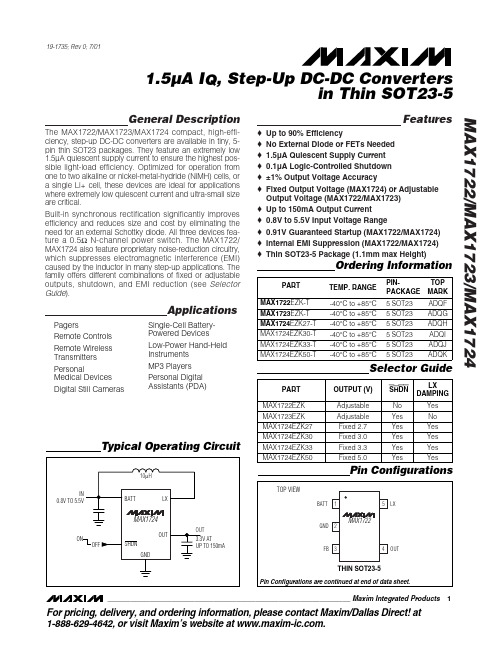
MAX1722
FB 3
4
OUT
THIN SOT23-5
Pin Configurations are continued at end of data sheet.
________________________________________________________________ Maxim Integrated Products
元器件交易网
19-1735; Rev 0; 7/01
1.5µA IQ, Step-Up DC-DC Converters in Thin SOT23-5
General Description
The MAX1722/MAX1723/MAX1724 compact, high-efficiency, step-up DC-DC converters are available in tiny, 5pin thin SOT23 packages. They feature an extremely low 1.5µA quiescent supply current to ensure the highest possible light-load efficiency. Optimized for operation from one to two alkaline or nickel-metal-hydride (NiMH) cells, or a single Li+ cell, these devices are ideal for applications where extremely low quiescent current and ultra-small size are critical. Built-in synchronous rectification significantly improves efficiency and reduces size and cost by eliminating the need for an external Schottky diode. All three devices feature a 0.5Ω N-channel power switch. The MAX1722/ MAX1724 also feature proprietary noise-reduction circuitry, which suppresses electromagnetic interference (EMI) caused by the inductor in many step-up applications. The family offers different combinations of fixed or adjustable outputs, shutdown, and EMI reduction (see Selector Guide). o o o o o o o o o o o
MAX2632EUK-T中文资料

ISM Radios
Wireless Local Loops
TV Tuners
Land Mobile Radios
Set-Top Boxes
__________Typical Operating Circuit
ON OFF
SHDN BIAS GND
CBLOCK
IN
IN
BIAS RBIAS
OUT
OUT
1.25:1
RBIAS = 40kΩ
1.3
1.5
VCC = 3V, TA = +25°C
5.5
6.5
8.0
Supply Current
RBIAS =10kΩ VCC = 3V, TA = TMIN to TMAX (Note1) 4.2
6.5
9.2
mA
VCC = 2.7V to 5.5V, TA = +25°C
PINPACKAGE
SOT TOP MARK*
MAX2630EUS-T -40°C to +85°C 4 SOT143
DG_ _
MAX2631EUK-T -40°C to +85°C 5 SOT23-5 AABK
MAX2632EUK-T -40°C to +85°C 5 SOT23-5 AABL
MAX2633EUT-T -40°C to +85°C 6 SOT23-6 AAAA
The MAX2630 comes in a 4-pin SOT143 package, requiring minimal board space. The MAX2631/MAX2632 come in small 5-pin SOT23 packages. The MAX2633 comes in a 6-pin SOT23 package.
MAXIM 化数字电位器MAX5481, MAX5482, MAX5483, MAX548 说明书

ENGLISH•简体中文•日本語•概述状况状况:生产中。
下载Notes MAX5481Linear13-WireSerial SPINon-Volatile102410253519.6$1.95@1kMAX548250$1.95 @1kMAX548310$1.95 @1kMAX548450$1.95 @1k查看所有Digital Potentiometers (128)引脚配置相关产品MAX5494,MAX5495,MAX5496, ...10位、双路、非易失、线性变化数字电位器类似产品:浏览其它类似产品线查看所有Digital Potentiometers (128产品)顶标MAX5481顶标MAX5482顶标MAX5483顶标MAX5484新品发布[ 2005-08-03 ]应用工程师帮助选型,下个工作日回复参数搜索应用帮助概述技术文档定购信息概述关键特性应用/使用关键指标图表注释、注解相关产品数据资料应用笔记评估板设计指南可靠性报告软件/模型价格与供货样品在线订购封装信息无铅信息参考文献: 19-3708 Rev. 4; 2008-03-12本页最后一次更新: 2008-03-27联络我们:信息反馈、提出问题 • 对该网页的评价 • 发送本网页 • 隐私权政策 • 法律声明 © 2010 Maxim Integrated Products版权所有General DescriptionThe MAX5481–MAX5484 10-bit (1024-tap) nonvolatile,linear-taper, programmable voltage-dividers and vari-able resistors perform the function of a mechanical potentiometer, but replace the mechanics with a pin-configurable 3-wire serial SPI™-compatible interface or up/down digital interface. The MAX5481/MAX5482 are 3-terminal voltage-dividers and the MAX5483/MAX5484are 2-terminal variable resistors.The MAX5481–MAX5484 feature an internal, non-volatile, electrically erasable programmable read-only memory (EEPROM) that stores the wiper position for ini-tialization during power-up. The 3-wire SPI-compatible serial interface allows communication at data rates up to 7MHz. A pin-selectable up/down digital interface is also available.The MAX5481–MAX5484 are ideal for applications requiring digitally controlled potentiometers. Two end-to-end resistance values are available (10k Ωand 50k Ω) in a voltage-divider or a variable-resistor configuration (see the Selector G uide ). The nominal resistor temperature coefficient is 35ppm/°C end-to-end, and only 5ppm/°C ratiometric, making these devices ideal for applications requiring low-temperature-coefficient voltage-dividers,such as low-drift, programmable gain-amplifiers.The MAX5481–MAX5484 operate with either a +2.7V to +5.25V single power supply or ±2.5V dual power sup-plies. These devices consume 400µA (max) of supply current when writing data to the nonvolatile memory and 1.0µA (max) of standby supply current. The MAX5481–MAX5484 are available in a space-saving (3mm x 3mm), 16-pin TQFN, or a 14-pin TSSOP pack-age and are specified over the extended (-40°C to +85°C) temperature range.ApplicationsFeatures♦1024 Tap Positions♦Power-On Recall of Wiper Position from Nonvolatile Memory♦16-Pin (3mm x 3mm x 0.8mm) TQFN or 14-Pin TSSOP Package♦35ppm/°C End-to-End Resistance Temperature Coefficient♦5ppm/°C Ratiometric Temperature Coefficient ♦10kΩand 50kΩEnd-to-End Resistor Values♦Pin-Selectable SPI-Compatible Serial Interface or Up/Down Digital Interface ♦1µA (max) Standby Current♦Single +2.7V to +5.25V Supply Operation ♦Dual ±2.5V Supply OperationMAX5481–MAX548410-Bit, Nonvolatile, Linear-Taper DigitalPotentiometers________________________________________________________________Maxim Integrated Products1Ordering InformationPin Configurations19-3708; Rev 5; 4/10For pricing delivery, and ordering information please contact Maxim Direct at 1-888-629-4642,or visit Maxim’s website at .Selector Guide appears at end of data sheet.SPI is a trademark of Motorola, Inc.temperature range.+Denotes a lead(Pb)-free/RoHS-compliant package.*EP = Exposed pad.Ordering Information continued at end of data sheet.Gain and Offset AdjustmentLCD Contrast Adjustment Pressure SensorsLow-Drift Programmable Gain AmplifiersMechanical Potentiometer ReplacementM A X 5481–M A X 548410-Bit, Nonvolatile, Linear-Taper Digital PotentiometersABSOLUTE MAXIMUM RATINGSStresses beyond those listed under “Absolute Maximum Ratings” may cause permanent damage to the device. These are stress ratings only, and functional operation of the device at these or any other conditions beyond those indicated in the operational sections of the specifications is not implied. Exposure to absolute maximum rating conditions for extended periods may affect device reliability.V DD to GND...........................................................-0.3V to +6.0V V SS to GND............................................................-3.5V to +0.3V V DD to V SS .............................................................-0.3V to +6.0V H, L, W to V SS ..................................(V SS - 0.3V) to (V DD + 0.3V)CS , SCLK(INC ), DIN(U/D ), SPI/UD to GND..-0.3V to (V DD + 0.3V)Maximum Continuous Current into H, L, and WMAX5481/MAX5483.........................................................±5mA MAX5482/MAX5484......................................................±1.0mA Maximum Current into Any Other Pin...............................±50mAContinuous Power Dissipation (T A = +70°C)16-Pin TQFN (derate 17.5mW/°C above +70°C).....1398.6mW 14-Pin TSSOP (derate 9.1mW/°C above +70°C)..........727mW Operating Temperature Range ...........................-40°C to +85°C Junction Temperature......................................................+150°C Storage Temperature Range.............................-60°C to +150°C Lead Temperature (soldering, 10s).................................+300°C Soldering Temperature (reflow).......................................+260°CELECTRICAL CHARACTERISTICSMAX5481–MAX548410-Bit, Nonvolatile, Linear-Taper DigitalPotentiometers_______________________________________________________________________________________3ELECTRICAL CHARACTERISTICS (continued)(V DD = +2.7V to +5.25V, V SS = V GND = 0V, V H = V DD , V L = 0V, T A = -40°C to +85°C, unless otherwise noted. Typical values are at V DD = +5.0V, T A = +25°C, unless otherwise noted.) (Note 1)M A X 5481–M A X 548410-Bit, Nonvolatile, Linear-Taper Digital Potentiometers 4_______________________________________________________________________________________TIMING CHARACTERISTICSNote 2:The DNL and INL are measured with the device configured as a voltage-divider with H = V DD and L = V SS . The wiper termi-nal (W) is unloaded and measured with a high-input-impedance voltmeter.Note 3:The DNL_R and INL_R are measured with D.N.C. unconnected and L = V SS = 0V. For V DD = +5V, the wiper terminal is dri-ven with a source current of I W = 80µA for the 50k Ωdevice and 400µA for the 10k Ωdevice. For V DD = +3V, the wiper termi-nal is driven with a source current of 40µA for the 50k Ωdevice and 200µA for the 10k Ωdevice.Note 4:The wiper resistance is measured using the source currents given in Note 3.Note 5:The device draws higher supply current when the digital inputs are driven with voltages between (V DD - 0.5V) and (V GND +0.5V). See Supply Current vs. Digital Input Voltage in the Typical Operating Characteristics .Note 6:Wiper settling test condition uses the voltage-divider configuration with a 10pF load on W. Transition code from 00000 00000to 01111 01111 and measure the time from CS going high to the wiper voltage settling to within 0.5% of its final value.MAX5481–MAX548410-Bit, Nonvolatile, Linear-Taper DigitalPotentiometers_______________________________________________________________________________________5-1.0-0.6-0.8-0.2-0.40.200.40.80.61.002563841285126407688961024DNL vs. CODE (MAX5483)CODED N L (L S B )V DD = 2.7V-1.0-0.6-0.8-0.2-0.40.200.40.80.61.002563841285126407688961024DNL vs. CODE (MAX5483)CODED N L (L S B )V DD = 5V-2.0-1.0-1.50-0.50.51.01.5 2.0INL vs. CODE (MAX5483)I N L (L S B )V DD = 2.7V02563841285126407688961024CODE-2.0-1.0-1.50-0.50.51.01.5 2.0INL vs. CODE (MAX5483)I N L (L S B )V DD = 3V2563841285126407688961024CODE-2.0-1.0-1.50-0.50.51.01.5 2.0INL vs. CODE (MAX5483)I N L (L S B )V DD = 5V02563841285126407688961024CODE-1.0-0.6-0.8-0.2-0.40.200.40.80.61.002563841285126407688961024DNL vs. CODE (MAX5481)CODED N L (L S B )-1.0-0.6-0.8-0.2-0.40.200.40.80.61.002563841285126407688961024DNL vs. CODE (MAX5481)CODED N L (L S B )V DD = 5V-1.0-0.6-0.8-0.2-0.40.200.40.80.61.002563841285126407688961024INL vs. CODE (MAX5481)CODEI N L (L S B )-1.0-0.6-0.8-0.2-0.40.200.40.80.61.002563841285126407688961024INL vs. CODE (MAX5481)CODEI N L (L S B )Typical Operating Characteristics(V DD = 5.0V, V SS = 0V, T A = +25°C, unless otherwise noted.)M A X 5481–M A X 548410-Bit, Nonvolatile, Linear-Taper Digital Potentiometers 6_______________________________________________________________________________________-1.0-0.6-0.8-0.2-0.40.200.40.80.61.002563841285126407688961024DNL vs. CODE (MAX5484)CODED N L (L S B )-1.0-0.6-0.8-0.2-0.40.200.40.80.61.002563841285126407688961024DNL vs. CODE (MAX5484)CODED N L (L S B )-1.0-0.6-0.8-0.2-0.40.200.40.80.61.002563841285126407688961024INL vs. CODE (MAX5484)CODEI N L (L S B )-1.0-0.6-0.8-0.2-0.40.200.40.80.61.002563841285126407688961024INL vs. CODE (MAX5484)CODEI N L (L S B )-1.0-0.6-0.8-0.2-0.40.200.40.80.61.002563841285126407688961024DNL vs. CODE (MAX5482)CODED N L (L S B )-1.0-0.6-0.8-0.2-0.40.200.40.80.61.002563841285126407688961024DNL vs. CODE (MAX5482)CODED N L (L S B )-1.0-0.6-0.8-0.2-0.40.200.40.80.61.002563841285126407688961024INL vs. CODE (MAX5482)CODEI N L (L S B )V DD = 2.7V-1.0-0.6-0.8-0.2-0.40.200.40.80.61.02563841285126407688961024INL vs. CODE (MAX5482)CODEI N L (L S B )V DD = 5V02010403050607080WIPER RESISTANCE vs. CODE (VARIABLE RESISTOR, T A = -40°C)M A X 5481 t o c 18R W (Ω)2563841285126407688961024CODETypical Operating Characteristics (continued)(V DD = 5.0V, V SS = 0V, T A = +25°C, unless otherwise noted.)MAX5481–MAX5484Typical Operating Characteristics (continued)(V DD = 5.0V, V SS = 0V, T A = +25°C, unless otherwise noted.)10-Bit, Nonvolatile, Linear-Taper DigitalPotentiometers_______________________________________________________________________________________702010403050607080WIPER RESISTANCE vs. CODE (VARIABLE RESISTOR, T A = +25°C)M A X 5481 t oc 19R W (Ω)2563841285126407688961024CODE2010403050607080WIPER RESISTANCE vs. CODE (VARIABLE RESISTOR, T A = +85°C)M A X 5481 t o c 20R W (Ω)2563841285126407688961024CODE10302050604070W-TO-L RESISTANCE vs. CODE(MAX5484)R W L (k Ω)02563841285126407688961024CODE02641012814W-TO-L RESISTANCE vs. CODE(MAX5483)R W L (k Ω)2563841285126407688961024CODE18.018.519.019.520.020.521.021.522.0012345WIPER RESISTANCE vs. WIPER VOLTAGE(VARIABLE RESISTOR)WIPER VOLTAGE (V)R W (Ω)-2.0-1.5-1.0-0.500.51.01.52.0-40-1510356085END-TO-END (R HL ) % CHANGE vs. TEMPERATURE (VOLTAGE-DIVIDER)M A X 5481 t o c 24TEMPERATURE (°C)E N D -T O -E N D R E S I S T A N C E C H A N G E (%)-2.0-1.5-1.0-0.500.51.01.52.0-40-1510356085WIPER-TO-END RESISTANCE (R WL ) % CHANGE vs. TEMPERATURE (VARIABLE RESISTOR)TEMPERATURE (°C)W I P E R -T O -E N D R E S I S T A N C E C H A N G E (%)00.30.90.61.21.5-4010-15356085STANDBY SUPPLY CURRENTvs. TEMPERATURETEMPERATURE (°C)I D D (μA )DIGITAL SUPPLY CURRENT vs. DIGITAL INPUT VOLTAGEDIGITAL INPUT VOLTAGE (V)I D D (μA )4.54.03.53.02.52.01.51.00.5110100100010,0000.15.0M A X 5481–M A X 548410-Bit, Nonvolatile, Linear-Taper Digital Potentiometers Typical Operating Characteristics (continued)(Circuit of Figure 1, T A = +25°C, unless otherwise noted.)1μs/divTAP-TO-TAP SWITCHING TRANSIENTRESPONSE (MAX5481)V W(AC-COUPLED)20mV/divCS 2V/divH = V DD , L = GND C W = 10pFFROM CODE 01 1111 1111TO CODE 10 0000 00004μs/divTAP-TO-TAP SWITCHING TRANSIENTRESPONSE (MAX5482)V W(AC-COUPLED)20mV/divCS 2V/divH = V DD , L = GND C W = 10pFFROM CODE 01 1111 1111TO CODE 10 0000 0000WIPER RESPONSE vs. FREQUENCY(MAX5481)FREQUENCY (kHz)G A I N (d B )100101-20-15-10-5-250.11000WIPER RESPONSE vs. FREQUENCY(MAX5482)FREQUENCY (kHz)G A I N (d B )100101-20-15-10-50-250.11000THD+N vs. FREQUENCY(MAX5481)FREQUENCY (kHz)T H D +N (%)1010.10.0010.010.11100.00010.01100THD+N vs. FREQUENCY(MAX5482)FREQUENCY (kHz)T H D +N (%)1010.10.0010.010.11100.00010.0110004020806012010014018016020002563841285126407688961024RATIOMETRIC TEMPERATURE COEFFICIENT vs. CODECODER A T I O M E T R I C T E M P C O (p p m )100300200500600400700VARIABLE-RESISTOR TEMPERATURECOEFFICIENT vs. CODET C V R (p p m )02563841285126407688961024CODE10-Bit, Nonvolatile, Linear-Taper DigitalPotentiometersPin DescriptionMAX5481–MAX5484M A X 5481–M A X 548410-Bit, Nonvolatile, Linear-Taper Digital Potentiometers Pin Description (continued)(MAX5483/MAX5484 Variable Resistors)MAX5481–MAX548410-Bit, Nonvolatile, Linear-Taper DigitalPotentiometersFunctional DiagramsM A X 5481–M A X 548410-Bit, Nonvolatile, Linear-Taper Digital Potentiometers Detailed DescriptionThe MAX5481/MAX5482 linear programmable voltage-dividers and the MAX5483/MAX5484 variable resistors feature 1024 tap points (10-bit resolution) (see the Functional Diagrams ). These devices consist of multi-ple strings of equal resistor segments with a wiper con-tact that moves among the 1024 points through a pin-selectable 3-wire SPI-compatible serial interface or up/down interface. The MAX5481/MAX5483 provide a total end-to-end resistance of 10k Ω, and the MAX5482/MAX5484 have an end-to-end resistance of 50k Ω. The MAX5481/MAX5482 allow access to the high, low, and wiper terminals for a standard voltage-divider configuration.MAX5481/MAX5482 ProgrammableVoltage-DividersThe MAX5481/MAX5482 programmable voltage-dividers provide a weighted average of the voltage between the H and L inputs at the W output. Both devices feature 10-bit resolution and provide up to 1024 tap points between the H and L voltages. Ideally,the V L voltage occurs at the wiper terminal (W) when all data bits are zero and the V H voltage occurs at the wiper terminal when all data bits are one. The step size (1 LSB) voltage is equal to the voltage applied across terminals H and L divided by 210. Calculate the wiper voltage V Was follows:Functional Diagrams (continued)MAX5481–MAX548410-Bit, Nonvolatile, Linear-Taper DigitalPotentiometerswhere D is the decimal equivalent of the 10 data bits writ-ten (0 to 1023), V HL is the voltage difference between the H and L terminals:The MAX5481 includes a total end-to-end resistance value of 10k Ωwhile the MAX5482 features an end-to-end resistance value of 50k Ω. These devices are not intended to be used as a variable resistor . Wiper cur-rent creates a nonlinear voltage drop in series with the wiper. To ensure temperature drift remains within speci-fications, do not pull current through the voltage-divider wiper. Connect the wiper to a high-impedance node.Figures 1 and 2 show the behavior of the MAX5481’s resistance from W to H and from W to L. This does not apply to the variable-resistor devicesMAX5483/MAX5484 Variable ResistorsThe MAX5483/MAX5484 provide a programmable resistance between W and L. The MAX5483 features a total end-to-end resistance value of 10k Ω, while the MAX5484 provides an end-to-end resistance value of 50k Ω. The programmable resolution of this resistance is equal to the nominal end-to-end resistance divided by 1024 (10-bit resolution). For example, each nominal segment resistance is 9.8Ωand 48.8Ωfor the MAX5483and the MAX5484, respectively.wiper position from the 1024 possible positions, result-ing in 1024 values for the resistance from W to L.Calculate the resistance from W to L (R WL ) by using the where D is decimal equivalent of the 10 data bits writ-ten, R W-L is the nominal end-to-end resistance, and R Z is the zero-scale error. Table 1 shows the values of R WL at selected codes for the MAX5483/MAX5484.Digital InterfaceConfigure the MAX5481–MAX5484 by a pin-selectable,3-wire, SPI-compatible serial data interface or an up/down interface. Drive SPI/UD high to select the 3-wire SPI-compatible interface. Pull SPI/UD low to select the up/down interface.V FSE V andV ZSE V FSE HL ZSE HL =⎡⎣⎢⎤⎦⎥=⎡⎣⎢⎤⎦⎥10241024,Figure 1. Resistance from W to H vs. Code (10k ΩVoltage-Divider)Figure 2. Resistance from W to L vs. Code (10k ΩVoltage-Divider)M A X 5481–M A X 548410-Bit, Nonvolatile, Linear-Taper Digital Potentiometers SPI-Compatible Serial InterfaceDrive SPI/UD high to enable the 3-wire SPI-compatible serial interface (see Figure 3). This write-only interface contains three inputs: chip select (CS ), data in (DIN(U/D )), and data clock (SCLK(INC )). Drive CS low to load the data at DIN(U/D ) synchronously into the shift register on each SCLK(INC ) rising edge.The WRITE command (C1, C0 = 00) requires 24 clock cycles to transfer the command and data (Figure 4a).The COPY commands (C1, C0 = 10 or 11) use either eight clock cycles to transfer the command bits (Figure 4b) or 24 clock cycles with the last 16 data bits disre-garded by the device.After loading the data into the shift register, drive CS high to latch the data into the appropriate control regis-ter. Keep CS low during the entire serial data stream to avoid corruption of the data. Table 2 shows the com-mand decoding.Write Wiper RegisterData written to this register (C1, C0 = 00) controls the wiper position. The 10 data bits (D9–D0) indicate the position of the wiper. For example, if DIN(U/D ) = 00 00000000, the wiper moves to the position closest to L. If DIN(U/D ) = 11 1111 1111, the wiper moves closest to H.This command writes data to the volatile random access memory (RAM), leaving the NV register unchanged. When the device powers up, the data stored in the NV register transfers to the wiper register,moving the wiper to the stored position. Figure 5 shows how to write data to the wiper register.Table 2. Command Decoding*X = Don’t care.Figure 3. SPI-Compatible Serial-Interface Timing Diagram (SPI/UD = 1)10-Bit, Nonvolatile, Linear-Taper DigitalPotentiometers ArrayMAX5481–MAX5484Figure4. Serial SPI-Compatible Interface FormatFigure5. Write Wiper Register OperationM A X 5481–M A X 548410-Bit, Nonvolatile, Linear-Taper Digital Potentiometers Copy Wiper Register to NV RegisterThe copy wiper register to NV register command (C1,C0 = 10) stores the current position of the wiper to the NV register for use at power-up. Figure 6 shows how to copy data from wiper register to NV register. The oper-ation takes up to 12ms (max) after CS goes high to complete and no other operation should be performed until completion.Copy NV Register to Wiper RegisterThe copy NV register to wiper register (C1, C0 = 11)restores the wiper position to the current value stored in the NV register. Figure 7 shows how to copy data from the NV register to the wiper register.Digital Up/Down InterfaceFigure 8 illustrates an up/down serial-interface timing diagram. In digital up/down interface mode (SPI/UD =0), the logic inputs CS , DIN(U/D ), and SCLK(INC ) con-trol the wiper position and store it in nonvolatile memory (see Table 3). The chip-select (CS ) input enables the serial interface when low and disables the interface when high. The position of the wiper is stored in the nonvolatile register when CS transitions from low to high while SCLK(INC ) is high.When the serial interface is active (CS low), a high-to-low (falling edge) transition on SCLK(INC ) increments or decrements the internal 10-bit counter depending on the state of DIN(U/D ). If DIN(U/D ) is high, the wiper increments. If DIN(U/D ) is low, the wiper decrements.The device stores the value of the wiper position in the nonvolatile memory when CS transitions from low to high while SCLK(INC ) is high. The host system can disablethe serial interface and deselect the device without stor-ing the latest wiper position in the nonvolatile memory by keeping SCLK(INC ) low while taking CS high.Upon power-up, the MAX5481–MAX5484 load the value of nonvolatile memory into the wiper register, and set the wiper position to the value last stored.Figure 6. Copy Wiper Register to NV Register OperationFigure 7. Copy NV Register to Wiper Register OperationMAX5481–MAX548410-Bit, Nonvolatile, Linear-Taper DigitalPotentiometersStandby ModeThe MAX5481–MAX5484 feature a low-power standby mode. When the device is not being programmed, it enters into standby mode and supply current drops to 0.5µA (typ).Nonvolatile MemoryThe internal EEPROM consists of a nonvolatile register that retains the last value stored prior to power-down.The nonvolatile register is programmed to midscale at the factory. The nonvolatile memory is guaranteed for 50 years of wiper data retention and up to 200,000wiper write cycles.Power-UpUpon power-up, the MAX5481–MAX5484 load the data stored in the nonvolatile wiper register into the volatile wiper register, updating the wiper position with the data stored in the nonvolatile wiper register.Applications InformationThe MAX5481–MAX5484 are ideal for circuits requiring digitally controlled adjustable resistance, such as LCD contrast control (where voltage biasing adjusts the dis-play contrast), or programmable filters with adjustable gain and/or cutoff frequency.Positive LCD Bias ControlFigures 9 and 10 show an application where a voltage-divider or a variable resistor is used to make an adjustable, positive LCD-bias voltage. The op amp pro-vides buffering and gain to the voltage-divider network made by the programmable voltage-divider (Figure 9) or to a fixed resistor and a variable resistor (see Figure 10).Programmable Gain and Offset AdjustmentFigure 11 shows an application where a voltage-divider and a variable resistor are used to make a programma-ble gain and offset adjustment.Figure 8. Up/Down Serial-Interface Timing Diagram (SPI/UD = 0)M A X 5481–M A X 548410-Bit, Nonvolatile, Linear-Taper Digital Potentiometers 18______________________________________________________________________________________Programmable FilterFigure 12 shows the configuration for a 1st-order pro-grammable filter using two variable resistors. Adjust R2for the gain and adjust R3 for the cutoff frequency. Use the following equations to estimate the gain (G) and the 3dB cutoff frequency (f C):Figure 10. Positive LCD Bias Control Using a Variable ResistorFigure 12. Programmable FilterFigure 11. Programmable Gain/Offset AdjustmentFigure 9. Positive LCD Bias Control Using a Voltage-DividerMAX5481–MAX548410-Bit, Nonvolatile, Linear-Taper DigitalPotentiometers______________________________________________________________________________________19Chip InformationPROCESS: BiCMOSSelector GuidePin Configurations (continued)Ordering Information (continued)Note: All devices are specified over the -40°C to +85°C operating temperature range.+Denotes a lead(Pb)-free/RoHS-compliant package.*EP = Exposed pad.Package InformationFor the latest package outline information and land patterns, go to /packages . Note that a “+”, “#”, or “-” in the package code indicates RoHS status only. Package draw-ings may show a different suffix character, but the drawing per-tains to the package regardless of RoHS status.M A X 5481–M A X 548410-Bit, Nonvolatile, Linear-Taper Digital Potentiometers Maxim cannot assume responsibility for use of any circuitry other than circuitry entirely embodied in a Maxim product. No circuit patent licenses are implied. Maxim reserves the right to change the circuitry and specifications without notice at any time.20____________________Maxim Integrated Products, 120 San Gabriel Drive, Sunnyvale, CA 94086 408-737-7600©2010 Maxim Integrated ProductsMaxim is a registered trademark of Maxim Integrated Products, Inc.。
MAX5921AEVKIT中文资料

19-2971; Rev 0; 8/03
MAX5921A Evaluation Kit
General Description
The MAX5921A evaluation kit (EV kit) is a fully assembled and tested surface-mount circuit board that provides current-limiting and multilevel fault protection using the MAX5921A hot-swap controller. The EV kit demonstrates the autoretry, configurable input undervoltage, overvoltage, and overcurrent monitoring features of the MAX5921A. The MAX5921A controls an external N-channel MOSFET to provide load-current regulation. The EV kit circuit undervoltage and overvoltage thresholds are configured to -32V and -80V, respectively, which makes the EV kit well suited for -48V telecom systems. The input operating voltage range is -20V to -80V (-48V rail systems). The EV kit is designed to withstand -100V input transients. The current-limiting threshold is configured for 1.8A output current. The EV kit can also be used to evaluate different versions of the MAX5920, MAX5921, or MAX5939 hotswap controllers after removing the MAX5921A. The MAX5920A/B are pin- and function-compatible with the LT4250 hot-swap controllers and pin-compatible with LT1640. Warning: The MAX5921A EV kit is designed to operate with high voltages. Dangerous voltages are present on this EV kit and on equipment connected to it. Users who power up this EV kit or power the sources connected to it must be careful to follow safety procedures appropriate to working with high-voltage electrical equipment. Under severe fault or failure conditions, this EV kit may dissipate large amounts of power, which could result in the mechanical ejection of a component or of component debris at high velocity. Operate this kit with care to avoid possible personal injury. The EV kit user should not probe the circuit with an oscilloscope probe and ground clip unless they have “high-voltage, hot-swap experience.”
SF5928S_规格书_v1.1
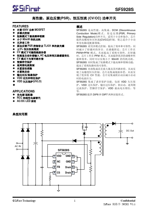
Confidential SiFirst_规格书_5928S_V1.1
工作温度范围 储存温度范围 ESD 人体模型 ESD 机器模型
推荐工作条件(注释 5)
VDD 工作范围 环境工作温度范围 最高工作开关频率
参数
SF5928S
-40 to 85
oC
-65 to 150
oC
3
kV
250
V
参数范围
Vth_OC
最大峰值电流
TD_OC
电流比较器关断延迟
功率 MOSFET 部分(注释 7)
BVdss
内部功率管 Drain 耐
压
Rdson
内部功率管阻抗
Idss Td(on)
内部功率管关断漏电 流 开通延迟
注释 6 I(Drain)=1A
©SiFirst Technology
-4-
最小 典型 最大 单位
DIP8
2
7
3
6
4
5
GND GND Drain Drain
VDD NC FB CS
1
7
DIP7 2
3
6
4
5
GND
Drain Drain
订购信息
订购型号
SF5928SDP SF5928SEP
IC 打印
SF5928SDP SF5928SEP
DIP8 DIP7
封装
RoHs RoHs
包装编带
最大输出功率 (1) 料号
输出电压 Vo
PFM 模式
PWM+PFM 模式
±5%
恒压模式
恒压CV模式
恒恒流流模C式C模式
自自动动恢重复启保护
电子元器件芯片

深圳市明烽威电子有限公司HCPL-4506-300E AVAGO HCPL-0600-500E AVAGOHCPL-4506-500E AVAGO HEDS-9701#C54AVAGOHCPL-4534-000E AVAGO TLC04CP TIHCPL-4534-300E AVAGO X9313WSZ-3T1INTERSILHCPL-4534-500E AVAGO TMS320LF2402APGA TIHCPL-4562-000E AVAGO TMS320LF2406APZA TIHCPL-4562-300E AVAGO AD9910BSVZ ADIHCPL-4562-500E AVAGO AD9957BSVZ ADIHCPL-4661-000E AVAGO TLV320AIC33IRGZ TIHCPL-4661-300E AVAGO TLV320AIC33IZQER TIHCPL-4661-500E AVAGO TPS54616PWPR TIHCPL-4731-000E AVAGO OPA551PA TIHCPL-4731-300E AVAGO DS1813R-15+DALLASHCPL-4731-500E AVAGO TPS7333QDR TIHCPL-7510-000E AVAGO OPA277UA TIHCPL-7510-300E AVAGO LM1877MX-9NSHCPL-7510-500E AVAGO ISO7221BDR TIHCPL-7520-000E AVAGO TL16C550CIPTR TIHCPL-7520-300E AVAGO MAX9324EUP+MAXIMHCPL-7520-500E AVAGO MAX1706EEE-T MAXIMHCPL-7560-000E AVAGO TPS75733KTTR TIHCPL-7560-300E AVAGO LM2674MX-ADJ NSHCPL-7560-500E AVAGO ADS8321EB TIHCPL-7611-000E AVAGO ADS8320EB TIHCPL-7611-300E AVAGO W29C040T-90B WINBONDHCPL-7611-500E AVAGO ISO124U TIHCPL-7710-000E AVAGO FM25L04B-GTR RAMTRONHCPL-7710-300E AVAGO TLE2084CN TIHCPL-7710-500E AVAGO TL317CDR TIHCPL-7720-000E AVAGO MAX354CPE+MAXIMHCPL-7720-300E AVAGO MAX354EPE+MAXIMHCPL-7720-500E AVAGO DEI0429-WMB DEIHCPL-7721-000E AVAGO AT91SAM7SE512-AU atmelHCPL-7721-300E AVAGO EL1881CSZ-T7INTERSILHCPL-7721-500E AVAGO SN74ACT2440FNR TIHCPL-7723-000E AVAGO MT4LC8M8C2P-5MICRONHCPL-7723-300E AVAGOHCPL-7800-000E AVAGOHCPL-7800-300E AVAGOHCPL-7800-500E AVAGOHCPL-7800A-000E AVAGOHCPL-7800A-300E AVAGOHCPL-7800A-500E AVAGOHCPL-7840-000E AVAGOHCPL-7840-300E AVAGOHCPL-7840-500E AVAGOHCPL786J-000E AVAGO HCPL-786J-000E AVAGO HCPL786J-300E AVAGO HCPL-786J-300E AVAGO HCPL786J-500E AVAGO HCPL-786J-500E AVAGO HCPL788J-000E AVAGO HCPL-788J-000E AVAGO HCPL788J-300E AVAGO HCPL-788J-300E AVAGO HCPL788J-500E AVAGO HCPL-788J-500EHCPL-817-000EHCPL-817-00AEHCPL-817-00BEHCPL-817-00CEHCPL-817-00DEHCPL-817-00LEHCPL-817-060EHCPL-817-06AEHCPL-817-06BEHCPL-817-06CEHCPL-817-06DEHCPL-817-06LEHCPL-817-300EHCPL-817-30AEHCPL-817-30BEHCPL-817-30CEHCPL-817-30DEHCPL-817-30LEHCPL-817-360EHCPL-817-36AEHCPL-817-36BEHCPL-817-36CEHCPL-817-36DEHCPL-817-36LEHCPL-817-500EHCPL-817-50AEHCPL-817-50BEHCPL-817-50CEHCPL-817-50DEHCPL-817-50LEHCPL-817-560EHCPL-817-56AEHCPL-817-56BEHCPL-817-56CEHCPL-817-56DEHCPL-817-56LEHCPL-9000-000E AVAGO DRV101FKTWT TIHCPL-9000-300E AVAGO DRV101F TIHCPL-9000-500E AVAGO UCC5638FQPR TIHCPL-902J-000E AVAGO TLV320AIC3204IRHBT TIHCPL-902J-300E AVAGO TLV320AIC3204IRHBR TIHCPL-902J-500E AVAGO TLV5625CDR TIHCPL-J312-000E AVAGO TLV5625IDR TIHCPL-J312-300E AVAGO TLV320AIC3104IRHBT TIHCPL-J312-500E AVAGO TLV320AIC3104IRHBR TIHCPL-J456-000E AVAGO AT45DB041D-SU ATMEL HCPL-J456-300E AVAGO MAX6657MSA+T MAXIM HCPL-J456-500E AVAGO HCPL-J454-000E AVAGO HCPL-M453-000E AVAGO HCPL-J454-300E AVAGO HCPL-M453-300E AVAGO HCPL-J454-400E AVAGO HCPL-M453-500E AVAGO HCPL-J454-500E AVAGO HCPL-M454-000E AVAGO HCPL-J454-600E AVAGO HCPL-M454-300E AVAGO TC7660IJA MICROCHIP HCPL-M454-500E AVAGO TC7660MJA MICROCHIP HCPL-M456-000E AVAGO ADT7460ARQZ ADIHCPL-M456-300E AVAGO ADSP-21065LKCA264ADIHCPL-M456-500E AVAGO ADSP-21065LKCAZ264ADI HCPL-M600-000E AVAGO AD7859ASZ ADI HCPL-M600-300E AVAGO MJD45H11G ONHCPL-M600-500E AVAGO TPD3E001DRLR TIHCPL-M601-000E AVAGO XTR116U TIHCPL-M601-300E AVAGO DS1233-5+DALLAS HCPL-M601-500E AVAGO TRU050GALGA32.0000/16.00Vectron HCPL-M611-000E AVAGO TRU050GACCA28.7040/14.35Vectron HCPL-M611-300E AVAGO AD9516-3BCPZ ADI HCPL-M611-500E AVAGO REF3125AIDBZT TIHCPL-M700-000E AVAGO REF3125AIDBZR TIHCPL-M700-300E AVAGO AD8592ARMZ ADI HCPL-M700-500E AVAGO QCPL-034H-500E AVAGOHD6413079F18HIT AD9865BCPZ ADI HDMP1636A AVAGO QCPL-312H-500E AVAGO HDMP-1636A AVAGO M74VHC1G135DFT1G ONHDMP-1637A AVAGO HSMD-A100-J00J1AVAGO HDMP1638AVAGO LT1587CT LTHDMP-1638AVAGO AD827JRZ-16ADI HEDS9710-R50AVAGO HSMP-389F-BLKG AVAGO HEDS-9710-R50AVAGO HSMP-389F-TR1G AVAGO HEL22MICREL HSMP-389F-TR2G AVAGO HEL23MICREL XC3064A-7PC84C XILINX HFBR-1414Z AVAGO XC3064A-7PC84I XILINX HFBR-1414TZ AVAGO Si7703EDN-T1-E3VISHAY HFBR-1521Z AVAGO Si7703EDN-T1-GE3VISHAYT-1521Z AVAGO Si7703EDN-T1-GE3ADIT-1521ETZ AVAGO AD605ARZ ADIHFBR-1521ETZ AVAGO MACH110-15JC AMDT-1522Z AVAGO MACH210-20JC AMDT-1522ETZ AVAGO LTC4213IDDB LINEAR HFBR-1522ETZ AVAGO DS1233-15+DALLAS HFBR1522Z AVAGO LTC3412EFE LINEAR HFBR-1522Z AVAGO MAX513ESD+T MAXIM HFBR1523Z AVAGO MAX3681EAG+MAXIM HFBR-1523Z AVAGO ICS1893CKILF IDT HFBR1528Z AVAGO TMS32C6416DGLZA5E0TI HFBR-1528Z AVAGO TMS32C6416EGLZ5E0TI HFBR-1531Z AVAGO TMS32C6416EGLZ6E3TI HFBR-1531ETZ AVAGO TMS32C6416EGLZ7E3TI HFBR-2531ETZ AVAGO TMS32C6416EGLZA5E0TI 1531ETZ AVAGO TMS32C6416EGLZA6E3TI 2531ETZ AVAGO AD829JRZ ADI HFBR1532Z AVAGO MAX14830ETM+MAXIM HFBR-1532Z AVAGO MX69GL128EAXGW-90G MXIC HFBR-1532ETZ AVAGO AD7811YRUZ ADI HFBR1533Z AVAGO TPS76318DBVR TI HFBR-1533Z AVAGO ADMP421ACEZ ADI HFBR-2412TZHFBR-2412ZHFBR2416TZHFBR-2416TZHFBR-2521Z AVAGO LT1304CS8Linear R-2521Z AVAGO MAX16801BEUA+T maxim R-2521ETZ AVAGO ACPL-M61L-500E AVAGO HFBR-2521ETZ AVAGO DS26503LN+DALLAS HFBR-2522Z AVAGO MAX9205EAI+T MAXIM R-2522Z AVAGO TMP105YZCT TIR-2522ETZ AVAGO TMP105YZCR TI HFBR-2522ETZ AVAGO AD5821BCBZ ADI HFBR-2523Z AVAGO PM5347-RI PMC HFBR-2528Z AVAGO PM73121-RI PMC HFBR-2531Z AVAGO TPA4411RTJT TI HFBR-2532Z AVAGO TPA4411RTJR TI HFBR-2532ETZ AVAGO LTC1438CG-ADJ Linear HFBR-2533Z AVAGO LTC1438IG-ADJ Linear HFBR-4501Z AVAGO DS1318E+DALLAS HFBR-4503Z AVAGO TMS320DM643AGDK5TI HFBR-4506Z AVAGO ACPL-M75L-000E AVAGO HFBR-4511Z AVAGO ACPL-M75L-060E AVAGO HFBR-4513Z AVAGO ACPL-M75L-500E AVAGO HFBR-4516Z AVAGO ACPL-M75L-560E AVAGO HFBR-4525Z AVAGO ACPL-T350-000E AVAGO HFBR-4526Z AVAGO ACPL-T350-060E AVAGO HFBR-4531Z AVAGO ACPL-T350-300E AVAGO HFBR-4532Z AVAGO ACPL-T350-360E AVAGOHFBR-4533Z AVAGO ACPL-T350-500E AVAGO HFBR-4535Z AVAGO ACPL-T350-560E AVAGO HFBR-4593Z AVAGO ADXRS620BBGZ ADI HFBR-4597Z AVAGO LT1521CS8Linear HFBR-EUD100Z AVAGO LT1521CS8-3.3Linear HFBR-EUD500Z AVAGO LT1521IS8Linear HFBR-EUS100Z AVAGO LT1521IS8-3.3Linear HFBR-EUS500Z AVAGO MAX6835VXSD3+T MAXIM HFBR-RUD100Z AVAGO AD9059BRSZ ADI HFBR-RUD500Z AVAGO HFBR-4515Z AVAGO HFBR-RUS100Z AVAGO HFBR-57E0PZ AVAGO HFBR-RUS500Z AVAGO HFCT-53D5EMZ AVAGO HG88510MITEL HFCT-5611AVAGOHI1-508-5HAR LT1242CS8Linear HI1-509-5HAR LT1242IS8Linear HM628512ALFP-5日立LT1140ACSW LinearHM628512BLFP-5日立AFBR-2419TZ AVAGO HS1101HUMIREL AD7156BCPZ ADIHS6118MACONICS ADP151ACBZ-2.8ADI HSDL-3201#021AVAGO DS1805Z-010+MAXIM HSDL-3201#001AVAGO TLP285-4GB TOSHIBA HSDL-3209-021AVAGO AD421BRZ ADI HSDL-7001#100AVAGO OPA2336PA TI HSDL-7002AVAGO ADUC812BSZ ADI HSMP-3814-BLKG AVAGO STPS6045CW ST HSMP-3814-TR1G AVAGO SG-3030JF EPSON HSMP-3814-TR2G AVAGO MPC8313VRAFFB FREESCAL HSMP-3822-BLKG AVAGO MAX1617AMEE+T maxim HSMP-3822-TR1G AVAGO MCP809M3X-4.63NS HSMP-3822-TR2G AVAGO MCP809M3X-4.38NS HSMP-3823-BLKG AVAGO MCP809M3X-4.00NS HSMP-3823-TR1G AVAGO MCP809M3X-3.08NS HSMP-3823-TR2G AVAGO MCP809M3X-2.93NS HSMP-3824-BLKG AVAGO MCP809M3X-2.63NS HSMP-3824-TR1G AVAGO MCP810M3X-4.63NS HSMP-3824-TR2G AVAGO MCP810M3X-4.38NS HSMP-3832-BLKG AVAGO MCP810M3X-4.00NS HSMP-3832-TR1G AVAGO MCP810M3X-3.08NS HSMP-3832-TR2G AVAGO MCP810M3X-2.93NS HSMP-3860-BLKG AVAGO MCP810M3X-2.63NS HSMP-3860-TR1G AVAGO LT1317BCS8Linear HSMP-3860-TR2G AVAGO LT1317BIS8Linear HSMP-3862-BLKG AVAGO LTC1757A-1EMS8Linear HSMP-3862-TR1G AVAGO ACPL-K342-000E AVAGO HSMP-3862-TR2G AVAGO ACPL-K342-500E AVAGO HSMP-3880-BLKG AVAGO AFBR-57M5APZ AVAGO HSMP-3880-TR1G AVAGO CY7C144AV-25AIT CY HSMP-3880-TR2G AVAGO CY7C144AV-25ACT CYHSMP-3892-BLKG AVAGO CY7C144AV-25AXIT CY HSMP-3892-TR1G AVAGO CY7C144AV-25AXCT CY HSMP-3892-TR2G AVAGO ABA-54563-TR1G AVAGO HSMP-389L-BLKG AVAGO ABA-54563-TR2G AVAGO HSMP-389L-TR1G AVAGO ABA-54563-BLKG AVAGO HSMP-389L-TR2G AVAGO LT1138ACG Linear HSMS-2812-BLKG AVAGO LT1138AIG Linear HSMS-2812-TR1G AVAGO ISL8120IRZ INTERSIL HSMS-2812-TR2G AVAGO ISL8120CRZ INTERSIL HSMS-2817-BLKG AVAGO LTC1421IG-2.5Linear HSMS-2817-TR1G AVAGO LTC1421CG-2.5Linear HSMS-2817-TR2G AVAGO MSC1212Y5PAGT TI HSMS-282K-BLKG AVAGO MSC1212Y5PAGR TI HSMS-282K-TR1G AVAGO TPS7330QDR TI HSMS-282K-TR2G AVAGO ADP3110KRZ ADI HSMS-2850-BLKG AVAGO MAX3263CAG MAXIM HSMS-2850-TR1G AVAGO MAX1729EUB MAXIM HSMS-2850-TR2G AVAGO MAX1651CSA MAXIM HSMS-8202-BLKG AVAGO AD876JR ADI HSMS-8202-TR1G AVAGO MAX1701EEE MAXIM HSMS-8202-TR2G AVAGO Si4201-BMR silicon HT2012-PL SMAR DS12C887+DALLAS HY62256ALT1-70HY LM236DR-2.5TIHY628100BLLG-70HY DS1722U DALLAS HY628100BLLG-70I HY LM7372MRX NSHY628400ALLG-55HY MAX490ESA+T MAXIM HY628400ALLG-70HY HSMS-2822-TR1G AVAGO HY62WT08081E-DG70C HY HSMP-389C-TR1G AVAGO HY62WT08081E-DG70I HY HSMP-389C-BLKG AVAGO ICL232IPE HAR HSMP-389C-TR2G AVAGO ICS8432DY-101ICS MC33375D-3.3R2G ONICS85322AM ICS AFBR-1529Z AVAGO ICS9112M-16ICS AFBR-2529Z AVAGO IDT75K62134S200BB IDT AFBR-1629Z AVAGO ILX139K SONY HSMS-2828-TR1G AVAGO IMP560ESA IMP TPS7101QDR TIIMP809JEUR-T IMP AFBR-57R5APZ AVAGO IMP809LEUR-T IMP UC3875DWPTR TIIMP809MEUR-T IMP ASSR-1510-503E AVAGO IMP809REUR-T IMP ASSR-1510-003E AVAGO IMP809SEUR-T IMP CY7B9514V-AC CYIMP809TEUR-T IMP MAX4450EXK+T MAXIM IMP810JEUR-T IMP SN75976A1DLR TIIMP810LEUR-T IMP ADUC831BSZ ADIIMP810MEUR-T IMP LTC1348IG LINEAR IMP810REUR-T IMP MSA-2111-TR1G AVAGO IMP810SEUR-T IMP DS1621S+T DALLAS IMP810TEUR-T IMP MAX485EESA+T MAXIMIMP811JEUS-T IMP MAX9669ETI+T MAXIM IMP811LEUS-T IMP MSA-0711-TR1G AVAGO IMP811MEUS-T IMP ACPL-P480-500E AVAGO IMP811REUS-T IMP HSMS-2800-TR1G AVAGO IMP811SEUS-T IMP LTC1622IS8LINEAR IMP811TEUS-T IMP MAX2102CWI MAXIM ACPL-312T-500E AVAGO X24165S-2.7T1XICOR ACPL-H342-560E AVAGO X84129SI-2.5T1XICOR ACPL-H342-500E AVAGO HCNW4502-500E AVAGO ACPL-H342-060E AVAGO HCNW4502-300E AVAGO ACPL-H342-000E AVAGO AD811ARZ-16ADI ACPL-K63L-500E AVAGO TOCP155TOSHIBA ACPL-K63L-560E AVAGO TOCP200TOSHIBA ACPL-K63L-000E AVAGO HFBR-14E4Z AVAGO AFBR-5803AQZ AVAGO HFBR-24E2Z AVAGO ASSR-4128-502E AVAGO ALM-2412-TR1G AVAGO HSMH-C680AVAGO TLV320DAC23GQER TIWS1403-TR1AVAGO CY2509ZXC-1T CYLST2825-T-SC AGILENT ACPL-312T-300E AVAGO MAX853ESA+T MAXIM MAX3814CHJ+T MAXIM。
- 1、下载文档前请自行甄别文档内容的完整性,平台不提供额外的编辑、内容补充、找答案等附加服务。
- 2、"仅部分预览"的文档,不可在线预览部分如存在完整性等问题,可反馈申请退款(可完整预览的文档不适用该条件!)。
- 3、如文档侵犯您的权益,请联系客服反馈,我们会尽快为您处理(人工客服工作时间:9:00-18:30)。
+60V Simple Swapper Hot-Swap Switch
General Description
The MAX5923 is a fully integrated Simple Swapper™ hot-swap switch for positive supply rails. The device allows the safe insertion and removal of circuit cards into live backplanes or ports without causing glitches on the power-supply rail. The device also monitors various circuit parameters and disconnects the load if a fault condition occurs, alerting the host with a logiclevel FAULT output. The MAX5923 operates over the +16V to +60V input voltage range. During startup, an integrated 0.45Ω power MOSFET regulates the current and voltage between the backplane power source and the load. After startup, the MOSFET is fully enhanced to reduce its on-resistance. To ensure robust operation, the MAX5923 contains built-in safety features that monitor fault conditions and prevent damage to the internal MOSFET. The MAX5923 monitors three parameters for fault conditions: zero current, overcurrent, and thermal overload. The output overcurrent limit counts the time the MAX5923 spends in an overcurrent condition and shuts down the pass transistor if the current limit is exceeded for the overcurrent time limit. The zero-current detection counts the time the output current is below the zero-current threshold and shuts down the pass transistor if the counter reaches the zero-current time limit. The thermal monitoring feature shuts down the pass transistor if the die temperature reaches the overtemperature limit. A fault logic output indicates when an overtemperature or an overcurrent condition has occurred and a zero-current logic output indicates if there is a zero-current condition. An undervoltage detection circuitry keeps the pass transistor off until the input voltage is above the undervoltage lockout (UVLO) threshold, which is internally set or can be set externally with a resistive divider. A power-OK (POK) output is provided to signal when the output voltage has reached to within 0.75V of the input voltage. An Enable input allows the host system to disconnect the system from the load and/or reset a fault condition by toggling Enable. The MAX5923 is available in a 20-pin TSSOP package and operates in the extended -40°C to +85°C temperature range. o 0.45Ω Integrated Power Switch o Programmable Output Current Up to 800mA o Over/Undercurrent-Limit Detection o Input Logic Signals Compatible with 1.8V to 5V CMOS Logic o Separate Analog and Digital Grounds with Up to ±4V Offset o Power-OK Status Output o Overcurrent Protection with Status Outputs o Built-In Thermal Shutdown o Internal Switch Protection Circuitry o Current-Limit Foldback with Timeout and DutyCycle Control o Latch or Autorestart Fault Management
+16V TO +60V IN RSENSE DRAIN VDIG RPU OUT D1 +1.65V TO +5.5V
MAX5923
UVLO LATCH RPU
ON OFF EN
ZC_EN RPU ZC FAULT POK AGND_S DGND
Applications
Network Routers/Switches Current Limiter Servers Industrial Equipment
ALL SIGNAL AND DIGITAL INPUTS/OUTPUTS ARE REFERENCED TO DGND. DGND CAN BE ±4V FROM AGND_S.
Simple Swapper is a trademark of Maxim Integrated Products, Inc.
Features
o Wide Operating Input Range: +16V to +60V
MAX5923
Ordering Information
PART MAX5923EUP TEMP RANGE -40°C to +85°C PIN-PACKAGE 20 TSSOP
Hale Waihona Puke Typical Operating Circuit
Pin Configuration appears at end of data sheet. 1
________________________________________________________________ Maxim Integrated Products
For pricing, delivery, and ordering information, please contact Maxim/Dallas Direct! at 1-888-629-4642, or visit Maxim’s website at .
/
+60V Simple Swapper Hot-Swap Switch MAX5923
ABSOLUTE MAXIMUM RATINGS
All Voltages with Respect to AGND_S, Unless Otherwise Noted IN ............................................................................-0.3V to +76V UVLO ........................................................................-0.3V to +6V VDIG to DGND .........................................................-0.3V to +6V OUT .......................................................-0.3V to (VDRAIN + 0.3V) DRAIN ..........................................................-0.3V to (VIN + 0.3V) EN, ZC_EN, ZC, FAULT, POK and LATCH to DGND ...............................................-0.3V to +6V DGND ..........................................................................-5V to +5V Maximum Current into DRAIN...............................................0.8A Maximum Current into POK, ZC, FAULT (sinking)..............20mA Continuous Power Dissipation (TA = +70°C) 20-Pin TSSOP (derate 11.1mW/°C above +70°C) .......879mW Operating Temperature Range ...........................-40°C to +85°C Junction Temperature ......................................................+150°C Storage Temperature Range .............................-65°C to +160°C Lead Temperature (soldering, 10s) .................................+300°C