CMHZ5226B中文资料
MPC5200B中文资料
Characteristics . . . . . . . . . . . . . . . . . . . . . . . 12 3.3 AC Electrical Characteristics . . . . . . . . . . . . 14 4 Package Description . . . . . . . . . . . . . . . . . . . . . . 61 4.1 Package Parameters . . . . . . . . . . . . . . . . . . 61 4.2 Mechanical Dimensions. . . . . . . . . . . . . . . . 61 4.3 Pinout Listings . . . . . . . . . . . . . . . . . . . . . . . 63
• Fast Ets 100Mbps IEEE 802.3 MII, 10 Mbps IEEE 802.3 MII, 10 Mbps 7-wire interface
• Universal Serial Bus Controller (USB) — USB Revision 1.1 Host — Open Host Controller Interface (OHCI) — Integrated USB Hub, with two ports.
sources — GPIO/Timer functions
– Up to 56 total GPIO pins (depending on functional multiplexing selections) that support a variety of interrupt/WakeUp capabilities.
MMSZ5265BT1中文资料
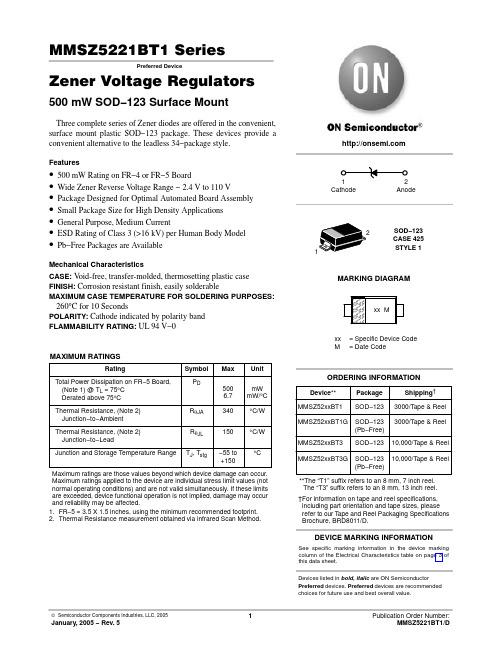
MMSZ5221BT1 SeriesPreferred DeviceZener Voltage Regulators 500 mW SOD−123 Surface MountThree complete series of Zener diodes are offered in the convenient, surface mount plastic SOD−123 package. These devices provide a convenient alternative to the leadless 34−package style.Features•500 mW Rating on FR−4 or FR−5 Board•Wide Zener Reverse V oltage Range − 2.4 V to 110 V •Package Designed for Optimal Automated Board Assembly •Small Package Size for High Density Applications •General Purpose, Medium Current•ESD Rating of Class 3 (>16 kV) per Human Body Model•Pb−Free Packages are AvailableMechanical CharacteristicsCASE:V oid-free, transfer-molded, thermosetting plastic case FINISH:Corrosion resistant finish, easily solderableMAXIMUM CASE TEMPERATURE FOR SOLDERING PURPOSES: 260°C for 10 SecondsPOLARITY:Cathode indicated by polarity band FLAMMABILITY RATING:UL 94 V−0MAXIMUM RATINGSMaximum ratings are those values beyond which device damage can occur. Maximum ratings applied to the device are individual stress limit values (not normal operating conditions) and are not valid simultaneously. If these limits are exceeded, device functional operation is not implied, damage may occur and reliability may be affected.1.FR−5 = 3.5 X 1.5 inches, using the minimum recommended footprint.2.Thermal Resistance measurement obtained via infrared Scan Method.See specific marking information in the device marking column of the Electrical Characteristics table on page 3 of this data sheet.DEVICE MARKING INFORMATIONDevices listed in bold, italic are ON Semiconductor Preferred devices. Preferred devices are recommended choices for future use and best overall value.ELECTRICAL CHARACTERISTICS (T A = 25°C unlessotherwise noted, V= 0.95 V Max. @ I = 10 mA)4.Nominal Zener voltage is measured with the device junction in thermal equilibrium at T L = 30°C $1°C.5.Z ZT and Z ZK are measured by dividing the AC voltage drop across the device by the ac current applied.The specified limits are for I Z(AC) = 0.1 I Z(dc) with the AC frequency = 1 KHz.V Z , NOMINAL ZENER VOLTAGE (V)−1012345678Figure 1. Temperature Coefficients (Temperature Range −55°C to +150°C)100101V Z , NOMINAL ZENER VOLTAGE (V)Figure 2. Temperature Coefficients (Temperature Range −55°C to +150°C)1.21.00.80.60.40.20T, TEMPERATURE (°C)Figure 3. Steady State Power Derating PW, PULSE WIDTH (ms)Figure 4. Maximum Nonrepetitive Surge Power1000100101V Z , NOMINAL ZENER VOLTAGEFigure 5. Effect of Zener Voltage onZener Impedance100101V F , FORWARD VOLTAGE (V)Figure 6. Typical Forward Voltage1000100101q V Z , T E M P E R A T U R E C O E F F I C I E N T (m V /°C )q V Z , T E M P E R A T U R E C O E F F I C I E N T (m V /°C )P p k , P E A K S U R G E P O W E R (W A T T S )Z Z T , D Y N A M I C I M P E D A N C E (W )I F , F O R W A R D C U R R E N T (m A )C , C A P A C I T A N C E (p F )V Z , NOMINAL ZENER VOLTAGE (V)Figure 7. Typical Capacitance 1000100101V Z , ZENER VOLTAGE (V)1001010.10.01V Z , ZENER VOLTAGE (V)1001010.10.01V Z , NOMINAL ZENER VOLTAGE (V)Figure 8. Typical Leakage CurrentFigure 9. Zener Voltage versus Zener Current(V Z Up to 12 V)Figure 10. Zener Voltage versus Zener Current(12 V to 91 V)I R , L E A K A G E C U R R E N T (m A )I Z , Z E N E R C U R R E N T (m A )I Z , Z E N E R C U R R E N T (m A )PACKAGE DIMENSIONSSOD−123CASE 425−04ISSUE Cǒmm inchesǓSCALE 10:1*For additional information on our Pb−Free strategy and solderingdetails, please download the ON Semiconductor Soldering and Mounting Techniques Reference Manual, SOLDERRM/D.SOLDERING FOOTPRINT*ON Semiconductor and are registered trademarks of Semiconductor Components Industries, LLC (SCILLC). SCILLC reserves the right to make changes without further notice to any products herein. SCILLC makes no warranty, representation or guarantee regarding the suitability of its products for any particular purpose, nor does SCILLC assume any liability arising out of the application or use of any product or circuit, and specifically disclaims any and all liability, including without limitation special, consequential or incidental damages.“Typical” parameters which may be provided in SCILLC data sheets and/or specifications can and do vary in different applications and actual performance may vary over time. All operating parameters, including “Typicals” must be validated for each customer application by customer’s technical experts. SCILLC does not convey any license under its patent rights nor the rights of others. SCILLC products are not designed, intended, or authorized for use as components in systems intended for surgical implant into the body, or other applications intended to support or sustain life, or for any other application in which the failure of the SCILLC product could create a situation where personal injury or death may occur. Should Buyer purchase or use SCILLC products for any such unintended or unauthorized application, Buyer shall indemnify and hold SCILLC and its officers, employees, subsidiaries, affiliates,and distributors harmless against all claims, costs, damages, and expenses, and reasonable attorney fees arising out of, directly or indirectly, any claim of personal injury or death associated with such unintended or unauthorized use, even if such claim alleges that SCILLC was negligent regarding the design or manufacture of the part. SCILLC is an Equal Opportunity/Affirmative Action Employer. This literature is subject to all applicable copyright laws and is not for resale in any manner.PUBLICATION ORDERING INFORMATION。
从内存条芯片编号看内存条的大小

从内存条芯片编号看内存条的大小(2009-11-22 08:12:39)转载▼标签:刷新速度tsop封装字段ddr266台湾itSDRAM 内存芯片的新编号HY XX X XX XX X X XX X X X-XX XA B C D E F G H I J K L MA字段由HY组成,代表现代(Hynix)内存芯片的前缀。
B字段表示产品类型。
57代表SDRAM内存。
C字段表示工作电压。
V代表VDD电压为3.3V、VDDQ电压为3.3V;Y代表VDD电压为3.0V、VDDQ电压为3.0v;U代表VDD电压为2.5V、VDDQ电压为2.5V;W代表VDD电压为2.5V、VDDQ电压为1.8V;S代表VDD电压为1.8V、VDDQ电压为1.8V/ D字段表示密度与刷新速度。
16代表16Mbit密度、2K刷新速度;32代表32Mbit密度、4K刷新速度;64代表64Mbit密度、4K刷新速度;28代表128Mbit密度、4K刷新速度;2A代表128Mbit密度(TCSR)、4K刷新速度;56代表256Mbit密度、8K刷新速度;12代表512Mbit密度、8K刷新速度。
E字段表示内存结构。
4代表x4;8代表x8;16代表x16 ;32代表x32。
F字段表示内存芯片内部由几个Bank组成。
1代表2Bank;2代表4Bank。
G字段表示电气接口。
0代表LVTTL;1代表SSTL_3。
H字段表示内存芯片的修正版本。
空白或H代表第1版;A或HA代表第2版;B或HB代表第3版;C或HC代表第4版。
也有一些特殊的编号规则,如:编号为HY57V64420HFT是第7版;编号为HY57V64420HGT和HY57V64820HGT是第8版;编号为HY57V28420AT是第3版;编号为HY57V56420HDT是第5版。
I字段表示功率消耗能力。
空白代表正常功耗;L代表代功耗;S代表超代功耗。
J字段表示内存芯片的封装方式。
ATMEL AT24C256B 说明书

BDTIC /ATMELTwo-wire SerialEEPROM256K (32,768 x 8)25279C–SEEPR–3/09AT24C256BFigure 1-1.Block Diagram 1.Absolute Maximum Ratings*Operating Temperature .....................................− 55°C to +125°C *NOTICE:Stresses beyond those listed under “Absolute Maximum Ratings” may cause permanent dam-age to the device. This is a stress rating only; functional operation of the device at these or any other conditions beyond those indicated in the operational sections of this specification is not implied. Exposure to absolute maximum rating conditions for extended periods may affect device reliability.Storage Temperature ........................................− 65°C to +150°C Voltage on Any Pinwith Respect to Ground .......................................− 1.0V to +7.0V Maximum Operating Voltage..........................................6.25V DC Output Current........................................................5.0 mA35279C–SEEPR–3/09AT24C256B2.Pin DescriptionSERIAL CLOCK (SCL): The SCL input is used to positive-edge clock data into each EEPROM device and negative-edge clock data out of each device.SERIAL DATA (SDA): The SDA pin is bidirectional for serial data transfer. This pin is open-drain driven and may be wire-ORed with any number of other open-drain or open-collector devices.DEVICE/PAGE ADDRESSES (A2, A1, A0): The A2, A1, and A0 pins are device address inputs that are hardwired (directly to GND or to Vcc) for compatibility with other AT24Cxx devices.When the pins are hardwired, as many as eight 256K devices may be addressed on a single bus system. (Device addressing is discussed in detail under “Device Addressing,” page 9.) A device is selected when a corresponding hardware and software match is true. If these pins are left floating, the A2, A1, and A0 pins will be internally pulled down to GND. However, due to capaci-tive coupling that may appear during customer applications, Atmel recommends always connecting the address pins to a known state. When using a pull-up resistor, Atmel recommends using 10k Ω or less.WRITE PROTECT (WP): The write protect input, when connected to GND, allows normal write operations. When WP is connected directly to Vcc, all write operations to the memory are inhib-ited. If the pin is left floating, the WP pin will be internally pulled down to GND. However, due to capacitive coupling that may appear during customer applications, Atmel recommends always connecting the WP pins to a known state. When using a pull-up resistor, Atmel recommends using 10k Ω or less.3.Memory OrganizationAT24C256B, 256K SERIAL EEPROM: The 256K is internally organized as 512 pages of 64bytes each. Random word addressing requires a 15-bit data word address.Note:1.This parameter is characterized and is not 100% tested.Table 3-1.Pin Capacitance (1)Applicable over recommended operating range from T A = 25°C, f = 1.0 MHz, V CC = +1.8VSymbol Test ConditionMax Units Conditions C I/O Input/Output Capacitance (SDA)8pF V I/O = 0V C IN Input Capacitance (A 0, A 1, SCL)6pFV IN = 0V45279C–SEEPR–3/09AT24C256BNotes:1.V IL min and V IH max are reference only and are not tested.Table 3-2.DC CharacteristicsApplicable over recommended operating range from: T AI = − 40°C to +85°C, V CC = +1.8V to +5.5V (unless otherwise noted)Symbol Parameter Test ConditionMin TypMax Units V CC1Supply Voltage 1.85.5V I CC1Supply Current V CC = 5.0V READ at 400 kHz 1.0 2.0mA I CC2Supply Current V CC = 5.0V WRITE at 400 kHz 2.0 3.0mA I SB1Standby Current (1.8V option)V CC = 1.8V V IN = V CC or V SS1.0µA V CC = 5.5V 6.0µA I LI Input Leakage Current V CC = 5.0V V IN = V CC or V SS 0.10 3.0µA I LO Output Leakage Current V CC = 5.0V V OUT = V CC or V SS0.053.0µA V IL Input Low Level (1)− 0.6V CC x 0.3V V IH Input High Level (1)V CC x 0.7V CC + 0.5V V OL2Output Low Level V CC = 3.0V I OL = 2.1 mA 0.4V V OL1Output Low LevelV CC = 1.8VI OL = 0.15 mA0.2V55279C–SEEPR–3/09AT24C256BNotes:1.This parameter is ensured by characterization and is not 100% tested.2.AC measurement conditions:R L (connects to V CC ): 1.3 k Ω (2.5V, 5.5V), 10 k Ω (1.8V)Input pulse voltages: 0.3 V CC to 0.7 V CC Input rise and fall times: ≤ 50 nsInput and output timing reference voltages: 0.5 V CCTable 3-3.AC Characteristics (Industrial Temperature)Applicable over recommended operating range from T AI = − 40°C to +85°C, V CC = +1.8V to +5.5V, CL = 100 pF (unless oth-erwise noted). Test conditions are listed in Note 2.Symbol Parameter1.8-volt2.5, 5.0-volt Units MinMax MinMax f SCL Clock Frequency, SCL 4001000kHz t LOW Clock Pulse Width Low 1.30.4µs t HIGH Clock Pulse Width High 0.60.4µs t i Noise Suppression Time (1)10050ns t AA Clock Low to Data Out Valid 0.050.90.050.55µs t BUF Time the bus must be free before a new transmission can start (1) 1.30.5µs t HD.STA Start Hold Time 0.60.25µs t SU.STA Start Set-up Time 0.60.25µs t HD.DAT Data In Hold Time 00µs t SU.DAT Data In Set-up Time 100100ns t R Inputs Rise Time (1)0.30.3µs t F Inputs Fall Time (1)300100ns t SU.STO Stop Set-up Time 0.60.25µs t DH Data Out Hold Time 5050ns t WRWrite Cycle Time 55ms Endurance (1)25°C, Page Mode, 3.3V1,000,000Write Cycles65279C–SEEPR–3/09AT24C256B4.Device OperationCLOCK and DATA TRANSITIONS: The SDA pin is normally pulled high with an external device. Data on the SDA pin may change only during SCL low time periods (see Figure 4-1).Data changes during SCL high periods will indicate a start or stop condition as defined below.Figure 4-1.Data ValiditySTART CONDITION: A high-to-low transition of SDA with SCL high is a start condition that must precede any other command (see Figure 4-2).Figure 4-2.Start and Stop DefinitionSTOP CONDITION: A low-to-high transition of SDA with SCL high is a stop condition. After a read sequence, the stop command will place the EEPROM in a standby power mode (see Fig-ure 4-2).ACKNOWLEDGE: All addresses and data words are serially transmitted to and from the EEPROM in 8-bit words. The EEPROM sends a “0” during the ninth clock cycle to acknowledge that it has received each word.STANDBY MODE: The AT24C256B features a low-power standby mode that is enabled uponpower-up and after the receipt of the stop bit and the completion of any internal operations.75279C–SEEPR–3/09AT24C256BSOFTWARE RESET: After an interruption in protocol, power loss or system reset, any 2-wire part can be protocol reset by following these steps: (a) Create a start bit condition, (b) clock 9cycles, (c) create another start bit followed by stop bit condition as shown below. The device is ready for next communication after above steps have been completed.Figure 4-3.Software ResetFigure 4-4.Bus TimingFigure 4-5.Write Cycle TimingNote:1.The write cycle time t WRis the time from a valid stop condition of a write sequence to the end of the internal clear/write cycle.85279C–SEEPR–3/09AT24C256BFigure 4-6.Output Acknowledge95279C–SEEPR–3/09AT24C256B5.Device AddressingThe 256K EEPROM requires an 8-bit device address word following a start condition to enable the chip for a read or write operation (see Figure 5-1). The device address word consists of a mandatory “1”, “0” sequence for the first four most significant bits as shown. This is common to all two-wire EEPROM devices.Figure 5-1.Device AddressThe next three bits are the A2, A1, A0 device address bits to allow as many as eight devices onthe same bus. These bits must compare to their corresponding hardwired input pins. The A2,A1, and A0 pins use an internal proprietary circuit that biases them to a logic low condition if the pins are allowed to float.The eighth bit of the device address is the read/write operation select bit. A read operation is ini-tiated if this bit is high, and a write operation is initiated if this bit is low.Upon a compare of the device address, the EEPROM will output a “0”. If a compare is not made,the device will return to a standby state.DATA SECURITY: The AT24C256B has a hardware data protection scheme that allows the user to write protect the whole memory when the WP pin is at V CC.105279C–SEEPR–3/09AT24C256B6.Write OperationsBYTE WRITE: A write operation requires two 8-bit data word addresses following the device address word and acknowledgment. Upon receipt of this address, the EEPROM will again respond with a “0” and then clock in the first 8-bit data word. Following receipt of the 8-bit data word, the EEPROM will output a “0”. The addressing device, such as a microcontroller, must then terminate the write sequence with a stop condition. At this time the EEPROM enters an internally-timed write cycle, t WR , to the nonvolatile memory. All inputs are disabled during this write cycle and the EEPROM will not respond until the write is complete (see Figure 6-1).Figure 6-1.Byte WriteNote:* = DON’T CARE bitPAGE WRITE: The 256K EEPROM is capable of 64-byte page writes.A page write is initiated the same way as a byte write, but the microcontroller does not send a stop condition after the first data word is clocked in. Instead, after the EEPROM acknowledges receipt of the first data word, the microcontroller can transmit up to 63 more data words. The EEPROM will respond with a “0” after each data word received. The microcontroller must termi-nate the page write sequence with a stop condition (see Figure 6-2).Figure 6-2.Page WriteNote:* = DON’T CARE bitThe data word address lower six bits are internally incremented following the receipt of each data word. The higher data word address bits are not incremented, retaining the memory page row location. When the word address, internally generated, reaches the page boundary, the fol-lowing byte is placed at the beginning of the same page. If more than 64 data words are transmitted to the EEPROM, the data word address will “roll over” and previous data will be overwritten. The address “roll over” during write is from the last byte of the current page to the first byte of the same page.ACKNOWLEDGE POLLING: Once the internally-timed write cycle has started and the EEPROM inputs are disabled, acknowledge polling can be initiated. This involves sending a start condition followed by the device address word. The read/write bit is representative of the operation desired. Only if the internal write cycle has completed will the EEPROM respond witha “0”, allowing the read or write sequence to continue.115279C–SEEPR–3/09AT24C256B7.Read OperationsRead operations are initiated the same way as write operations with the exception that the read/write select bit in the device address word is set to “1”. There are three read operations:current address read, random address read, and sequential read.CURRENT ADDRESS READ: The internal data word address counter maintains the last address accessed during the last read or write operation, incremented by one. This address stays valid between operations as long as the chip power is maintained. The address “roll over”during read is from the last byte of the last memory page, to the first byte of the first page.Once the device address with the read/write select bit set to “1” is clocked in and acknowledged by the EEPROM, the current address data word is serially clocked out. The microcontroller does not respond with an input “0” but does generate a following stop condition (see Figure 7-1).Figure 7-1.Current Address ReadRANDOM READ: A random read requires a “dummy” byte write sequence to load in the data word address. Once the device address word and data word address are clocked in and acknowledged by the EEPROM, the microcontroller must generate another start condition. The microcontroller now initiates a current address read by sending a device address with the read/write select bit high. The EEPROM acknowledges the device address and serially clocks out the data word. The microcontroller does not respond with a “0” but does generate a following stop condition (see Figure 7-2).Figure 7-2.Random ReadNote:*= DON’T CARE bit125279C–SEEPR–3/09AT24C256BSEQUENTIAL READ: Sequential reads are initiated by either a current address read or a ran-dom address read. After the microcontroller receives a data word, it responds with an acknowledge. As long as the EEPROM receives an acknowledge, it will continue to increment the data word address and serially clock out sequential data words. When the memory address limit is reached, the data word address will “roll over” and the sequential read will continue. The sequential read operation is terminated when the microcontroller does not respond with a “0” but does generate a following stop condition (see Figure 7-3).Figure 7-3.Sequential Read135279C–SEEPR–3/09AT24C256B8.AT24C256B Ordering CodesNotes:1.“-B” denotes bulk.2.“-T” denotes tape and reel. SOIC = 4K per reel. TSSOP and dBGA2 = 5K per reel. SAP = 3K per reel. EIAJ = 2K per reel.3.Available in tape & reel and wafer form; order as SL788 for inkless wafer form. Bumped die available upon request. Pleasecontact Serial Interface Marketing.Ordering CodeVoltage Package Operation RangeAT24C256B-PU (Bulk Form Only)AT24C256BN-SH-B (1) (NiPdAu Lead Finish)AT24C256BN-SH-T (2) (NiPdAu Lead Finish)AT24C256BW-SH-B (1) (NiPdAu Lead Finish)AT24C256BW-SH-T (2) (NiPdAu Lead Finish)AT24C256B-TH-B (1) (NiPdAu Lead Finish)AT24C256B-TH-T (2) (NiPdAu Lead Finish)AT24C256BY7-YH-T (2) (NiPdAu Lead Finish)AT24C256BU2-UU-T (2) 1.81.81.81.81.81.81.81.81.88P38S18S18S28S28A28A28Y78U2-1Lead-free/Halogen-free Industrial Temperature (−40°C to 85°C)AT24C256B-W-11 1.8Die SaleIndustrial Temperature (−40°C to 85°C)Package Type8P38-lead, 0.300" Wide, Plastic Dual Inline Package (PDIP)8S18-lead, 0.150" Wide, Plastic Gull Wing Small Outline Package (JEDEC SOIC)8S28-lead, 0.200” Wide, Plastic Gull Wing Small Outline Package (EIAJ SOIC)8U2-18-ball, die Ball Grid Array Package (dBGA2)8A28-lead, 4.40 mm Body, Plastic Thin Shrink Small Outline Package (TSSOP)8Y78-lead, 6.00 mm x 4.90 mm Body, Ultra Thin, Dual Footprint, Non-leaded, Small Array Package (SAP)Options−1.8Low-voltage (1.8V to 5.5V)145279C–SEEPR–3/09AT24C256B9.Part Marking Scheme 8-PDIP8-SOICTOP MARKSeal YearY = SEAL YEARWW = SEAL WEEK | Seal Week6: 2006 0: 2010 02 = Week 2 | | |7: 2007 1: 2011 04 = Week 4 |---|---|---|---|---|---|---|---| 8: 2008 2: 2012 :: : :::: : A T M L U Y W W 9: 2009 3: 2013:: : :::: :: |---|---|---|---|---|---|---|---| 50 = Week 50 2 E B 152 = Week 52|---|---|---|---|---|---|---|---| * Lot NumberLot Number to Use ALL Characters in Marking |---|---|---|---|---|---|---|---| |BOTTOM MARKPin 1 Indicator (Dot)No Bottom MarkTOP MARKSeal YearY = SEAL YEARWW = SEAL WEEK | Seal Week6: 2006 0: 2010 02 = Week 2 | | |7: 2007 1: 2011 04 = Week 4 |---|---|---|---|---|---|---|---| 8: 2008 2: 2012 :: : :::: : A T M L H Y W W 9: 2009 3: 2013:: : :::: :: |---|---|---|---|---|---|---|---| 50 = Week 50 2 E B 152 = Week 52|---|---|---|---|---|---|---|---| * Lot NumberLot Number to Use ALL Characters in Marking |---|---|---|---|---|---|---|---| |BOTTOM MARKPin 1 Indicator (Dot)No Bottom Mark155279C–SEEPR–3/09AT24C256B8-TSSOP8-Ultra Thin SAPTOP MARKPin 1 Indicator (Dot)Y = SEAL YEAR WW = SEAL WEEK |6: 2006 0: 2010 02 = Week 2 |---|---|---|---| 7: 2007 1: 2011 04 = Week 4 * H Y W W 8: 2008 2: 2012 :: : :::: : |---|---|---|---|---| 9: 2009 3: 2013:: : :::: :: 2 E B 1 50 = Week 50 |---|---|---|---|---| 52 = Week 52BOTTOM MARKXX = Country of Origin |---|---|---|---|---|---|---| X X|---|---|---|---|---|---|---| A A A A A A A |---|---|---|---|---|---|---| <- Pin 1 IndicatorTOP MARKSeal Year| Seal Week Y = SEAL YEARWW = SEAL WEEK | | |6: 2006 0: 2010 02 = Week 2 |---|---|---|---|---|---|---|---| 7: 2007 1: 2011 04 = Week 4 A T M L H Y W W 8: 2008 2: 2012 :: : :::: : |---|---|---|---|---|---|---|---| 9: 2009 3: 2013:: : :::: :: 2 E B 150 = Week 50 |---|---|---|---|---|---|---|---| 52 = Week 52Lot Number|---|---|---|---|---|---|---|---| * |Pin 1 Indicator (Dot)165279C–SEEPR–3/09AT24C256BdBGA2TOP MARKLINE 1-------> 2EBU LINE 2-------> YMTC|<-- Pin 1 This CornerY = ONE DIGIT YEAR CODE 4: 2004 7: 20075: 2005 8: 20086: 2006 9: 2009M = SEAL MONTH (USE ALPHA DESIGNATOR A-L) A = JANUARY B = FEBRUARY " " """"""" J = OCTOBER K = NOVEMBER L = DECEMBERTC = TRACE CODE175279C–SEEPR–3/09AT24C256B10.Packaging Information 8P3 – PDIP185279C–SEEPR–3/09AT24C256B8S1 – JEDEC SOIC195279C–SEEPR–3/09AT24C256B205279C–SEEPR–3/09AT24C256B8U2-1 – dBGA2215279C–SEEPR–3/09AT24C256B8A2 – TSSOP225279C–SEEPR–3/09AT24C256B8Y7 – SAP235279C–SEEPR–3/09AT24C256BRevision HistoryDoc. Rev.Date Comments5279C 3/2009Changed the Vcc to 5.5V in the test condition for Isb15279B 3/2008Format changes to document5279A1/2008AT24C256B product with date code 2008 work week 14 (814) or later supports 5Vcc operation Initial document release。
CMS1620B 用户手册说明书

CMS1620B用户手册LED驱动控制专用电路V1.1请注意以下有关CMS知识产权政策*中微半导体公司已申请了专利,享有绝对的合法权益。
与中微半导体公司MCU或其他产品有关的专利权并未被同意授权使用,任何经由不当手段侵害中微半导体公司专利权的公司、组织或个人,中微半导体公司将采取一切可能的法律行动,遏止侵权者不当的侵权行为,并追讨中微半导体公司因侵权行为所受的损失、或侵权者所得的不法利益。
*中微半导体公司的名称和标识都是中微半导体公司的注册商标。
*中微半导体公司保留对规格书中产品在可靠性、功能和设计方面的改进作进一步说明的权利。
然而中微半导体公司对于规格内容的使用不负责任。
文中提到的应用其目的仅仅是用来做说明,中微半导体公司不保证和不表示这些应用没有更深入的修改就能适用,也不推荐它的产品使用在会由于故障或其它原因可能会对人身造成危害的地方。
中微半导体公司的产品不授权适用于救生、维生器件或系统中作为关键器件。
中微半导体公司拥有不事先通知而修改产品的权利,对于最新的信息,请参考我们的网站目录1.产品概述 (1)1.1功能特性 (1)1.2特性说明 (1)1.3管脚分布 (2)2.指令说明 (3)3.显示寄存器地址 (5)4.显示 (6)4.1驱动共阴数码管 (6)4.2驱动共阳极数码管 (7)5.键扫描和键扫数据寄存器 (8)6.按键 (9)6.1按键扫描 (9)7.串行数据传输格式 (11)8.应用时串行数据的传输 (12)8.1地址增加模式 (12)8.2固定地址模式 (12)8.3读按键时序 (13)8.4采用地址自动加一和固定地址方式的程序设计流程图 (14)9.应用电路 (16)10.电气参数 (18)11.封装 (20)11.1SOP20 (20)12.版本修订说明 (21)1. 产品概述1.1 功能特性CMS1620B是一种带键盘扫描接口的LED(发光二极管显示器)驱动控制专用电路,内部集成有MCU数字接口、数据锁存器、LED高压驱动、键盘扫描等电路。
rc522产品手册
rc522产品手册一、概述RC522是一款广泛应用的非接触式射频识别(RFID)读写器芯片,专为高频(13.56 MHz)射频通信设计。
由于其高效性能、低功耗及易于集成等特性,RC522在物联网、电子门锁、智能支付等领域有着广泛的应用。
本手册将详细介绍RC522的主要功能、技术规格、使用方法及常见问题解答。
二、产品特性工作频率:13.56 MHz。
支持ISO14443A/MIFARE标准。
高集成度:将射频前端、解调器、安全逻辑和EEPROM 存储器集成于单芯片中。
低功耗:在待机状态下电流消耗仅为170μA,读写时为3.3mA。
高速数据传输:支持高达848 kbps的通信速率。
多种接口选择:可与SPI、I2C、UART等接口进行连接。
安全性:支持加密和解密功能,确保数据传输的安全性。
三、使用方法硬件连接:根据所选接口,将RC522与微控制器或其他设备进行连接。
注意确保天线连接良好,以获得最佳的通信效果。
电源供应:为RC522提供稳定的电源,建议电压范围为3.3-5V。
寄存器配置:根据需求,通过SPI、I2C或UART接口对RC522的寄存器进行配置。
这包括设置通信参数、选择工作模式等。
读写操作:使用配置好的寄存器参数,对RFID标签进行读写操作。
数据处理:对从RFID标签读取的数据进行解码和安全性验证,确保数据的准确性和安全性。
四、常见问题及解答1.RC522支持哪些类型的RFID标签?答:RC522支持ISO14443A标准和MIFARE系列标签,可读写多种类型的RFID 标签。
2.为什么无法读取RFID标签?答:可能的原因包括天线连接不良、标签与读卡器之间的距离过远、存在干扰等。
请检查天线连接和工作环境,确保符合通信要求。
3.如何配置RC522的寄存器?答:根据需要,通过SPI、I2C或UART接口对RC522的寄存器进行配置。
具体配置方法可参考相关开发文档或手册。
IC 知 识 简 介

IC 知识简介IC知识一一、IC的分类IC按功能可分为:数字IC、模拟IC、微波IC及其他IC,其中,数字IC是近年来应用最广、发展最快的IC品种。
数字IC就是传递、加工、处理数字信号的IC,可分为通用数字IC和专用数字IC。
通用IC:是指那些用户多、使用领域广泛、标准型的电路,如存储器(DRAM)、微处理器(MPU)及微控制器(MCU)等,反映了数字IC的现状和水平。
专用IC(ASIC):是指为特定的用户、某种专门或特别的用途而设计的电路。
目前,集成电路产品有以下几种设计、生产、销售模式。
1.IC制造商(IDM)自行设计,由自己的生产线加工、封装,测试后的成品芯片自行销售。
2.IC设计公司(Fabless)与标准工艺加工线(Foundry)相结合的方式。
设计公司将所设计芯片最终的物理版图交给Foundry 加工制造,同样,封装测试也委托专业厂家完成,最后的成品芯片作为IC设计公司的产品而自行销售。
打个比方,Fabless相当于作者和出版商,而Foundry相当于印刷厂,起到产业"龙头"作用的应该是前者。
二、世界集成电路产业结构的变化及其发展历程自1958年美国德克萨斯仪器公司(TI)发明集成电路(IC)后,随着硅平面技术的发展,二十世纪六十年代先后发明了双极型和MOS型两种重要的集成电路,它标志着由电子管和晶体管制造电子整机的时代发生了量和质的飞跃,创造了一个前所未有的具有极强渗透力和旺盛生命力的新兴产业集成电路产业。
回顾集成电路的发展历程,我们可以看到,自发明集成电路至今40多年以来,"从电路集成到系统集成"这句话是对IC产品从小规模集成电路(SSI)到今天特大规模集成电路(ULSI)发展过程的最好总结,即整个集成电路产品的发展经历了从传统的板上系统(System-on-board)到片上系统(System-on-a-chip)的过程。
在这历史过程中,世界IC产业为适应技术的发展和市场的需求,其产业结构经历了三次变革。
atc中文手册
A T24C256中文资料2009-11-15 09:43特性与1MHz I2C 总线兼容1.8 到6.0 伏工作电压范围低功耗CMOS 技术写保护功能当WP 为高电平时进入写保护状态64 字节页写缓冲器自定时擦写周期100,000 编程/擦写周期可保存数据100 年8 脚DIP SOIC 封装温度范围商业级工业级和汽车级概述CAT24WC256 是一个256K 位串行CMOS E2PROM 内部含有32768 个字节每字节为8 位CATALYST 公司的先进CMOS 技术实质上减少了器件的功耗CAT24WC256 有一个64 字节页写缓冲器该器件通过I2C 总线接口进行操作管脚描述管脚名称功能A0 A1 地址输入SDA 串行数据/地址SCL 串行时钟WP 写保护Vcc +1.8V 6.0V 电源Vss 地NC 未连接极限参数工作温度工业级-55 +125商业级0 +75贮存温度-65 +150各管脚承受电压-2.0V Vcc+2.0VVcc 管脚承受电压-2.0V +7.0V封装功率损耗Ta=25 1.0W焊接温度(10 秒) 300口输出短路电流100mA功能描述CAT24WC256 支持I2C 总线数据传送协议I2C 总线协议规定任何将数据传送到总线的器件作为发送器任何从总线接收数据的器件为接收器数据传送是由产生串行时钟和所有起始停止信号的主器件控制的CAT24WC256 是作为从器件被操作的主器件和从器件都可以作为发送器或接收器但由主器件控制传送数据发送或接收的模式管脚描述SCL 串行时钟CAT24WC256 串行时钟输入管脚用于产生器件所有数据发送或接收的时钟这是一个输入管脚SDA 串行数据/地址双向串行数据/地址管脚用于器件所有数据的发送或接收SDA 是一个开漏输出管脚可与其它开漏输出或集电极开路输出进行线或wire-ORWP 写保护当WP 脚连接到Vcc 所有内存变成写保护只能读当WP 引脚连接到Vss 或悬空允许器件进行读/写操作A0 A1 器件地址输入这些管脚为硬连线或者不连接对于单总线系统最多可寻址4 个CAT24WC256 器件参阅器件寻址当这些引脚没有连接时其默认值为0I2C 总线协议I2C 总线协议定义如下1 只有在总线空闲时才允许启动数据传送2 在数据传送过程中当时钟线为高电平时数据线必须保持稳定状态不允许有跳变时钟线为高电平时数据线的任何电平变化将被看作总线的起始或停止信号起始信号时钟线保持高电平期间数据线电平从高到低的跳变作为I2C 总线的起始信号停止信号时钟线保持高电平期间数据线电平从低到高的跳变作为I2C 总线的停止信号器件寻址主器件通过发送一个起始信号启动发送过程然后发送它所要寻址的从器件的地址8 位从器件地址的高5 位固定为10100 见图5 接下来的2 位A1 A0 为器件的地址位最多可以连接4 个器件到同一总线上这些位必须与硬连线输入脚A1 A0 相对应从器件地址的最低位作为读写控制位1表示对从器件进行读操作0 表示对从器件进行写操作在主器件发送起始信号和从器件地址字节后CAT24WC256 监视总线并当其地址与发送的从地址相符时响应一个应答信号通过SDA 线CAT24WC256 再根据读写控制位R/W 的状态进行读或写操作应答信号I2C 总线数据传送时每成功地传送一个字节数据后接收器都必须产生一个应答信号应答的器件在第9 个时钟周期时将SDA 线拉低表示其已收到一个8 位数据CAT24WC256 在接收到起始信号和从器件地址之后响应一个应答信号如果器件已选择了写操作则在每接收一个8 位字节之后响应一个应答信号当CAT24WC256 工作于读模式时在发送一个8 位数据后释放SDA 线并监视一个应答信号一旦接收到应答信号CAT24WC256 继续发送数据如主器件没有发送应答信号器件停止传送数据并等待一个停止信号写操作字节写在字节写模式下主器件发送起始信号和从器件地址信息R/W 位置0 给从器件在从器件送回应答信号后主器件发送两个8 位地址字写入CAT24WC256 的地址指针主器件在收到从器件的应答信号后再发送数据到被寻址的存储单元CAT24WC256 再次应答并在主器件产生停止信号后开始内部数据的擦写在内部擦写过程中CAT24WC256 不再应答主器件的任何请求页写在页写模式下单个写周期内CAT24WC256 最多可以写入64 个字节数据页写操作的启动和字节写一样不同在于传送了一字节数据后主器件允许继续发送63 个字节每发送一个字节后CAT24WC256 将响应一个应答位且内部低6 位地址加1 高位地址保持不变如果主器件在发送停止信号之前发送大于64 个字节地址计数器将自动翻转先前写入的数据被覆盖当所有64 字节接收完毕主器件发送停止信号内部编程周期开始此时所有接收到的数据在单个写周期内写入CAT24WC256应答查询可以利用内部写周期时禁止数据输入这一特性一旦主器件发送停止位指示主器件操作结束时CAT24WC256 启动内部写周期应答查询立即启动包括发送一个起始信号和进行写操作的从器件地址如果CAT24WC256 正在进行内部写操作将不会发送应答信号如果CAT24WC256 已经完成了内部写操作将发送一个应答信号主器件可以继续对CAT24WC256 进行下一次读写操作写保护写保护操作特性可使用户避免由于不当操作而造成对存储区域内部数据的改写当WP 管脚接高时整个寄存器区全部被保护起来而变为只可读取CAT24WC256 可以接收从器件地址和字节地址但是装置在接收到第一个数据字节后不发送应答信号从而避免寄存器区域被编程改写读操作CAT24WC256 读操作的初始化方式和写操作时一样仅把R/W 位置为1 有三种不同的读操作方式立即/当前地址读选择/随机读和连续读立即/当前地址读的地址计数器内容为最后操作字节的地址加1 也就是说如果上次读/写的操作地址为N 则立即读的地址从地址N+1 开始如果N=E 此处E=32767 则计数器将翻转到0 且继续输出数据CAT24WC256接收到从器件地址信号后R/W 位置1 它首先发送一个应答信号然后发送一个8 位字节数据主器件不需发送一个应答信号但要产生一个停止信号选择/随机读选择/随机读操作允许主器件对寄存器的任意字节进行读操作主器件首先通过发送起始信号从器件地址和它想读取的字节数据的地址执行一个伪写操作在CAT24WC256 应答之后主器件重新发送起始信号和从器件地址此时R/W 位置1 CAT24WC256 响应并发送应答信号然后输出所要求的一个8 位字节数据主器件不发送应答信号但产生一个停止信号连续读连续读操作可通过立即读或选择性读操作启动在CAT24WC256 发送完一个8 位字节数据后主器件产生一个应答信号来响应告知CAT24WC256 主器件要求更多的数据对应每个主机产生的应答信号CAT24WC256 将发送一个8 位数据字节当主器件不发送应答信号而发送停止位时结束此操作从CAT24WC256 输出的数据按顺序由N 到N+1 输出读操作时地址计数器在CAT24WC256 整个地址内增加这样整个寄存器区域在可在一个读操作内全部读出当读取的字节超过E 此处E=32767计数器将翻转到零并继续输出数据字节。