AMS1117
ams1117热阻参数
ams1117热阻参数
AMS1117是一种线性稳压器,常用于电子电路中对电压进行稳定的应用。
热阻参数是指该芯片的热阻特性,即在芯片工作时,芯片内部产生的热量与芯片外部环境之间的热传导阻力。
根据AMS1117的规格手册,它的热阻参数为:
TO-252封装(也称为DPAK封装):θJA = 65°C/W
SOT-223封装:θJA = 100°C/W
其中,θJA表示芯片到环境的热阻,单位为°C/W。
这个数值表示每瓦特的功耗在芯片内部产生的温升与芯片外部环境之间的温度差。
例如,对于TO-252封装的AMS1117芯片,如果其功耗为1瓦特,则芯片内部温度将比环境温度高65°C。
需要注意的是,这些热阻参数是在特定的测试条件下测量得到的,实际应用中可能会因为环境条件、散热设计等因素而有所不同。
因此,在具体应用中,建议根据实际情况进行热设计和散热方案的选择。
1/ 1。
ams1117工作原理

ams1117工作原理AMS1117是一种低压差线性稳压器,广泛应用于电子设备中,以提供稳定的电压输出。
它的工作原理是基于反馈控制的负反馈电路。
在电子设备中,稳定的电压输出对于各种电路和元件的正常工作至关重要。
然而,电源的输出电压通常会受到电网波动、负载变化等因素的影响,导致输出电压不稳定。
为了解决这个问题,稳压器被引入到电源电路中。
AMS1117是一种线性稳压器,其工作原理基于反馈控制。
它的输入电压可以是较高的直流电压(通常为5V或12V),而输出电压可以是较低的直流电压(通常为3.3V或1.8V)。
稳压器的核心部件是一个差分放大器,它将输出电压与参考电压进行比较,并根据差值调整控制元件的工作状态。
具体而言,AMS1117内部包含了一个误差放大器、一个错误放大器、一个调节器和一个输出放大器。
误差放大器用于将输出电压与参考电压进行比较,得到一个误差信号。
错误放大器将误差信号放大,并通过调节器将其转换成控制信号。
调节器根据控制信号的大小调整输出电压,使其趋于稳定。
输出放大器将调整后的输出电压放大,以满足负载的需求。
在工作过程中,AMS1117通过内部反馈回路不断调整输出电压,使其保持在设定的数值范围内。
当输入电压或负载发生变化时,稳压器会自动调整输出电压,以保持其稳定性。
这种负反馈控制的机制能够有效地抵消外部影响,使得输出电压具有很高的稳定性和精确度。
除了稳定电压输出,AMS1117还具有过热保护和短路保护功能。
当温度超过一定限制或输出短路时,稳压器会自动切断输出,以防止损坏电路和元件。
AMS1117是一种基于反馈控制的低压差线性稳压器。
它通过内部的误差放大器、错误放大器、调节器和输出放大器等元件,实现了对输入电压的稳定调节和保护功能。
在电子设备中,AMS1117能够提供稳定的电压输出,保证各种电路和元件的正常工作。
AMS1117中文资料

SOT-223
SOT-89-3
TO-220-3L
特点
TO-263-3L
TO-252-2L
* 固定输出电压为 1.5V、1.8V、2.5V、2.85V、3.0V、 3.3V、5.0V 和可调版本,具有 1%的精度
* 固定输出电压为 1.2V 的 精度为 2% * 低漏失电压:1A 输出电流时仅为 1.2V * 限流功能 * 过热切断 * 温度范围:-40°C~ 125°C
0≤IOUT≤1A, 3.9V≤VIN ≤10V
2.450 2.500 2.550
(见下页)
ADVANCED MONOLITHIC SYSTEMS (translate by BONA 0755-82800289)
共10页 第3页
AMS1117
(接上页)
参数
V
0≤IOUT≤1A, 4.25V≤VIN ≤10V
2.790 2.850 2.910
0≤IOUT≤500mA, VIN =4.10V
2.790 2.850 2.910
AMS1117-3.0,
IOUT=10mA, VIN=4.5V,TJ=25°C , 2.970 3.000 3.030 V
VOUT 0≤IOUT≤1A, 4.4V≤VIN≤10V
2.940 3.000 3.060
AMS1117-3.3, IOUT=10mA, VIN=5V,TJ=25°C , 0≤IOUT≤1A, 4.75V≤VIN≤10V
3.267 3.300 3.333 V 3.235 3.300 3.365
AMS1117-5.0,
IOUT=10mA, VIN=7V, TJ=25°C , 4.950 5.000 5.05 V
ams1117工作原理

ams1117工作原理
ams1117是一种常用的线性稳压器,其工作原理是将输入电压稳定为固定的输出电压。
它是一种具有低压差和高稳定性的稳压器,适用于各种电子设备中。
ams1117的工作原理可以简单描述为输入电压经过稳压芯片内部的电路,经过一系列的处理后,输出固定的电压给负载。
这个过程可以分为几个关键步骤。
输入电压进入稳压芯片,经过电源输入端的滤波电容进行滤波处理,去除输入电压中的噪声和纹波,以确保稳定的输入电压。
接下来,输入电压经过稳压芯片内部的参考电压源和误差放大器,与参考电压进行比较,产生一个误差信号。
这个误差信号被送入控制电路,通过调节控制电路中的电流,控制输出电压的大小。
在控制电路中,误差信号经过放大和滤波处理,然后通过一个比较器和一个PWM(脉宽调制)控制器,在一定的周期内产生一个可调节的占空比。
这个占空比决定了输出电压的大小。
PWM控制器将控制信号发送给功率元件,功率元件通过控制电路中的电流,将输入电压转换为稳定的输出电压。
输出电压通过输出端的滤波电容进行滤波处理,去除输出电压中的噪声和纹波,以确保稳定的输出电压。
输出电压被连接到负载上,为负载提供稳定的电源。
总的来说,ams1117通过内部的电路和控制器,将输入电压稳定为固定的输出电压。
它具有低压差和高稳定性的特点,适用于各种电子设备中,如电源模块、无线通信设备、计算机等。
它的工作原理简单而可靠,能够为电子设备提供稳定可靠的电源。
AMS1117
最小值
1.238 1.225 1.782 1.764
典型值
1.25 1.25 1.80 1.80
最大值
1.262 1.275 1.818 1.836
单位
V V
2.475 2.45 2.822 2.793
2.5 2.5 2.85 2.85
2.525 2.55 2.878 2.907
V
Vout
输出电压
V
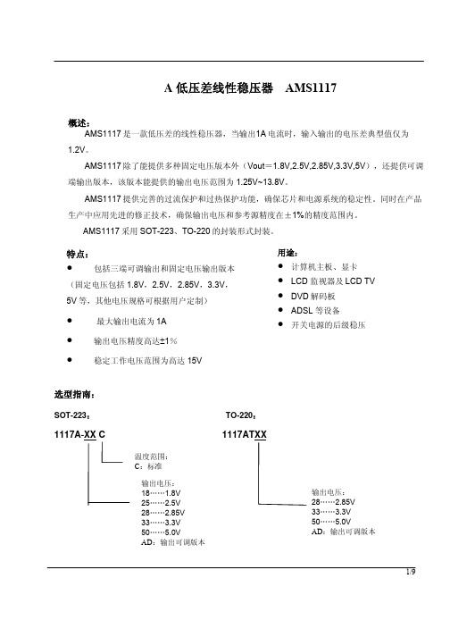
特点:
用途:
•
包括三端可调输出和固定电压输出版本
(固定电压包括 1.8V,2.5V,2.85V,3.3V, 5V 等,其他电压规格可根据用户定制)
• • •
最大输出电流为 1A 输出电压精度高达±1% 稳定工作电压范围为高达 15V
• • • • •
计算机主板、显卡 LCD 监视器及 LCD TV DVD 解码板 ADSL 等设备 开关电源的后级稳压
AMS1117-3.3V, Vin-Vout=1.25V
4
8
mA
AMS1117-5V, Vin-Vout=1.25V
4
8
mA
IAdj
可调端电流 (输出可调版)
55
120
uA
5/9
AMS1117
Ichange 可调端电流 变化 热稳定性 θJC 热阻 20 0.2 5 uA
0.5
% ℃/W
注释:
Note1:表中所给出的电压线性度和负载线性度的参数是在常温下测试的。负载线性度随温度的 变化曲线请参看后面的典型参数曲线。 Note2:常温下,当 Iout 在 0~1A 之间,Vin-Vout 在 1.5V 和 12V 之间变化时,满足表中给 出的规范范围。 Note3:输入输出电压差 Vdropout 是在如下条件下测试的,在各种输出电流值下,以 Vin=Vout+1.5V 时的输出电压 Vout 作为输出参考电压值,减小输入电压,当 Vout 的值 降低 1%时所对应的输入输出电压差即为 Vdropout。 Note4:最小负载电流是指当输入电压在如下范围内(1.5V≦Vin-Vout≦12V)变化时,为保证 Vout 的变化在规范范围内,对输出负载电流的要求。即要求负载电流不小于 10mA。
低压差稳压器--AMS1117芯片简介

低压差稳压器--AMS1117芯⽚简介结构从内部框图可以看出,ASM1117提供电流限制和热保护(TSD),以防环境温度造成过⾼的结温。
电路包含1个齐纳调节的带隙参考电压以确保输出电压的精度在±1%以内。
ADJ引脚是可调整电压引脚,⽤来接⼊可调电阻,调出你所需要的电压。
基本⼯作原理AMS1117是⼀个低漏失电压调整器,它的稳压调整管是由⼀个PNP驱动的NPN管组成的,漏失电压定义为: VDROP = VBE+ VSAT。
AMS1117有固定和可调两个版本可⽤,输出电压可以是:1.2V,1.5V,1.8V,2.5V,2.85V, 3.0V,3.3V,和5.0V。
⽚内过热切断电路提供了过载和过热保护,以防环境温度造成过⾼的结温。
LM1117有可调电压的版本,通过2个外部电阻可实现1.25~13.8V输出电压范围。
另外还有5个固定电压输出(1.8V、2.5V、2.85V、3.3V和5V)的型号。
X1117是⼀款正电压输出的低压降三端线性稳压电路,在1A输出电流下的压降为1.2V。
分为两个版本,固定电压输出版本和可调电压输出版本。
固定输出电压1.5V、1.8V、2.5V、3.3V、5.0V和可调版本的电压精度为1%;固定电压为1.2V的产品输出电压精度为2%。
内部集成过热保护和限流电路,适⽤于各类电⼦产品。
AMS1117-3.3参数:绝对最⼤额定值:20V⼯作结温范围:-40~125°C输⼊电压:15V焊接温度(25秒):265°C存储温度:-65~150°CAMS1117-3.3电⽓特性:输出电压:3.267~3.333V(0≤IOUT≤1A,4.75V≤VIN≤12V)线性调整(最⼤):10mV(4.75V≤VIN≤12V)负载调节(最⼤):15mV(VIN=5V,0≤IOUT≤1A)电压差(最⼤):1.3V电流限制:900~1500mA静态电流(最⼤):10mA纹波抑制(最⼩):60dB。
ams1117热阻参数

ams1117热阻参数【原创实用版】目录1.AMS1117 概述2.热阻参数的定义与意义3.AMS1117 的热阻参数特性4.AMS1117 的应用领域5.结论正文一、AMS1117 概述AMS1117 是一款由德州仪器(TI)公司推出的 1.2A 同步降压 DC-DC 转换器,具有出色的性能和效率。
这款器件采用了恒定频率电流模式控制,可以实现高达 98% 的转换效率。
在众多的电源管理器件中,AMS1117 以其稳定的输出电压和广泛的应用领域而受到广泛关注。
二、热阻参数的定义与意义热阻参数,又称热阻系数,是指在给定温度差下,通过器件的电流与产生的热量之间的比值。
热阻参数是衡量器件散热性能的重要指标,直接影响到器件的可靠性和稳定性。
对于电源管理器件而言,热阻参数尤为重要,因为它们通常工作在高功率和高温环境。
三、AMS1117 的热阻参数特性AMS1117 的热阻参数特性如下:1.温度范围:AMS1117 的工作温度范围为 -40℃至 125℃。
在此温度范围内,器件的性能和稳定性得到保证。
2.热阻系数:AMS1117 的热阻系数为 4.5°C/W。
这意味着在 1W 的功耗下,通过器件的电流每增加 1A,器件的温度将上升 4.5°C。
3.散热设计:由于 AMS1117 具有较高的热阻参数,因此在应用过程中需要合理设计散热方案,以保证器件的可靠性和稳定性。
四、AMS1117 的应用领域AMS1117 广泛应用于各种电源管理领域,如通信设备、工业控制、网络设备、便携式电子设备等。
在这些应用中,AMS1117 的热阻参数特性对于保证系统的稳定运行具有重要意义。
五、结论综上所述,AMS1117 作为一款优秀的电源管理器件,在拥有较高转换效率的同时,也具备良好的热阻参数特性。
AMS1117全系列
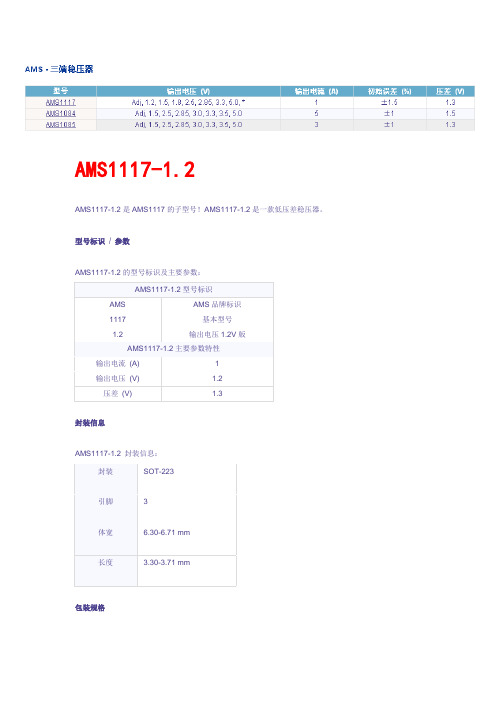
AMS1117-1.2AMS1117-1.2是AMS1117的子型号!AMS1117-1.2是一款低压差稳压器。
型号标识/ 参数AMS1117-1.2的型号标识及主要参数:AMS1117-1.2型号标识AMS AMS品牌标识1117 基本型号1.2 输出电压1.2V版AMS1117-1.2主要参数特性输出电流(A) 1输出电压(V) 1.2压差(V) 1.3封装信息AMS1117-1.2 封装信息:封装SOT-223引脚 3体宽 6.30-6.71 mm长度 3.30-3.71 mm包装规格AMS1117-1.2 包装规格:AMS1117-1.8AMS1117-1.8是AMS1117的子型号!AMS1117-1.8是一款低压差稳压器。
型号标识/ 参数AMS1117-1.8的型号标识和参数如下表所示:封装信息AMS1117-1.8的封装为:类型:SOT-223引脚:3体宽:6.30-6.71 mm长度:3.30-3.71 mm引脚间距:2.29 mm包装规格AMS1117-1.8的包装规格为:类型:Tape&Reel(卷带装)每盘:2,500 pcsAMS1117-2.5AMS1117-2.5是AMS1117的子型号!AMS1117-2.5是一款低压差稳压器。
型号标识/ 参数AMS1117-2.5的型号标识和参数如下表所示:封装信息AMS1117-2.5的封装为:类型:SOT-223引脚:3体宽:6.30-6.71 mm长度:3.30-3.71 mm引脚间距:2.29 mm包装规格AMS1117-2.5的包装规格为: 类型:Tape&Reel (卷带装) 每盘:2,500 pcsAMS1117-2.85AMS1117-2.85是AMS1117的子型号!AMS1117-2.85是一款低压差稳压器。
型号标识 / 参数AMS1117-2.85的型号标识及主要参数:封装信息AMS1117-2.85 封装信息:包装规格AMS1117-2.85 包装规格:AMS1117-3.3AMS1117-3.3是AMS1117的子型号!AMS1117-3.3是一款低压差稳压器。
- 1、下载文档前请自行甄别文档内容的完整性,平台不提供额外的编辑、内容补充、找答案等附加服务。
- 2、"仅部分预览"的文档,不可在线预览部分如存在完整性等问题,可反馈申请退款(可完整预览的文档不适用该条件!)。
- 3、如文档侵犯您的权益,请联系客服反馈,我们会尽快为您处理(人工客服工作时间:9:00-18:30)。
1A Adjustable/Fixed Low Dropout Linear Regulator- Low dropout voltage- Load regulation: 0.2% typical - Optimized for Low V oltage - On-chip thermal limiting- Standard SOT-223 and TO-252 packages- Three-terminal adjustable or fixed low dropout 1.2V ,1.5V ,1.8V , 2.5V , 2.85V , 3.3V , 5V . Regulators- Active SCSI terminators- High efficiency linear regulators- Post regulators for switching supplies - Battery chargers- 12V to 5V linear regulators - M otherboard clock suppliesThe AMS 1117-ADJ and AMS 1117-1.2,-1.5,-1.8,-2.5,-2.85, -3.3 and-5 are low dropout three-terminal regulators with 1A output current capability. These devices have been optimized for low voltage where transient response and minimum input voltage are critical. The 2.85V version is designed specifically to be used in Active Terminators for SCSI bus.On-chip thermal limiting provides protection against any combination of overload and ambient temperatures that would create excessive junction temperatures.Unlike PNP type regulators where up to 10% of the output current is wasted as quiescent current, the quiescent cur-rent of the AMS 1117 flows into the load, increasing effi-ciency.The AMS 1117 series regulators are available in the indus-try-standard SOT-223 and TO-252 power packages.Key FeaturesApplicationsGeneral DescriptionTypical ApplicationNotice: The distance between V out pin and Capacitor should not exceed 4cm for excellent performanceFigure 1. Typical Applications of AMS 11171A Adjustable/Fixed Low Dropout Linear RegulatorPin Assignments*With package soldered to 0.5 square inch copper area over backside ground plane or internal power plane, ΘJA can vary from 30°C/W to more than 50°C/W. Other mounting techniques may provide better thermal resistance than 30°C/W.Absolute Maximum RatingsFigure 2. Pin Assignments of AMS 1117ParameterMin.Max.UnitV IN 18 V(V IN – V OUT ) * I OUTSee Figure 3Operating Junction Temperature Range -20 125°C Storage Temperature Range-65150°C Lead Temperature (Soldering, 10 sec.) 300°C1A Adjustable/Fixed Low Dropout Linear RegulatorTypicals and limits appearing in normal type apply for T J =25℃.Limits appearing in Boldface type apply over the entire junction temperature for operation, -20℃to 125℃.Electrical CharacteristicBlock DiagramThermal LimitCurrent LimitV OUTV INSubstrateGND (fixed output) ADJ. (adjustable output)Figure 3. Block Diagram of AMS 1117SymbolParameterConditionsMin (Note 2) Typ (Note 1) Max(Note 2)UnitsV REFReference VoltageAMS 11171.5V<=(V IN -V OUT )<=7V,10mA<=I OUT <=1A1.225 1.250 1.275 VV OUT Output Voltage10mA<=I OUT <=1AI OUT = 10mA, V IN = 3.2V AMS 1117-1.2 ,2.7V<= V IN <=8.2V 1.176 1.152 1.200 1.200 1.224 1.248 V AMS 1117-1.5 ,3.0V<= V IN <=8.5V1.4701.5001.530VAMS 1117-1.8 ,3.3V<= V IN <=8.8V 1.764 1.800 1.836 VAMS 1117-2.5 ,4V<= V IN <= 9.5V 2.450 2.500 2.550 V AMS 1117-2.85 , 4.35V <= V IN <= 9.85V 2.793 2.850 2.907 V AMS 1117-3.3 , 4.8V<= V IN <=10.3V 3.234 3.300 3.366 V AMS 1117-5.0,6.5V<=V IN <= 12V4.9005.0005.100V1A Adjustable/Fixed Low Dropout Linear RegulatorTypicals and limits appearing in normal type apply for T J =25℃.Limits appearing in Boldface type apply over the entire junction temperature for operation, -20℃ to 125℃.Electrical Characteristic(Continued)Symbol ParameterConditionsMin (Note 2)Typ (Note 1) Max (Note 2) Units △V OUTLine Regultion (Note 3)I OUT =10mA ,(V OUT +1.5V)<=V IN <=12V 0.035 0.2 % Load Regultion (Note 3) V IN -V OUT =2V,10mA<= I OUT <=1A,0.2 0.7 % AMS 1117-1.2V IN -V OUT =2V,10mA<= I OUT <=1A,0.2 1 % V IN -V OUTDropout Volage I OUT =1A,△V REF =1% 1.100 1.250 V I LimitCurrent Limit V IN -V OUT = 2V, T J =25℃1.1 1.5A Minimum Load Current (Note 4) AMS 1117-ADJ1.5V<=(V IN -V OUT )<=10V10mA Quiescent CurentV IN =V OUT +1.25V 5 13 mA Thermal Regulation T A = 25°C, 30ms pulse 0.01 0.1 %/W RippleRejection f=120Hz,V IN -V OUT =3V, V Ripple =1V PP60 72 dB Adjust Pin Current50120µAAdjust Pin CurrentChange 1.5V<=V IN -V OUT <=7V, 10mA<=I OUT <=1A0.2 5 µATemperature Stability0.5 % Long Term StabilityT A = 125°C, 1000hrs.0.3%1A Adjustable/Fixed Low Dropout Linear RegulatorNote 1: Typical Values represent the most likely parametric norm. Note 2: All limits are guaranteed by testing or statistical analysis.Note 3: Load and line regulation are measured at constant junction room temperature. Note 4: The minimum output current required to maintain regulation.Typical Performance CharacteristicsTypicals and limits appearing in normal type apply for T J =25℃.Limits appearing in Boldface type apply over the entire junction temperature for operation, -20℃to 125℃.Electrical Characteristic(Continued)Symbol ParameterConditionsMin (Note 2) Typ (Note 1) Max (Note 2)UnitsI LimitRMS Output Noise(% ofV OUT )T A = 25°C, 10Hz<= f <=10kHz0.003 % Thermal Resistance, Junctionto CaseSOT-22315 ℃/W TO-252 3 ℃/W Thermal Shutdown Junction Temperature155 ℃ Thermal Shutdown Hysteresis25℃Output Current ( A )0 0.2 0.4 0.6 0.8 1.01.5 1.4 1.3 1.2 1.0 0.9 0.8 0.7 0.6 0.5 0D r o p o u t V o l t a g e ( V )Figure 4. Dropout Voltage VS. Output Current1A Adjustable/Fixed Low Dropout Linear RegulatorTypical Performance Characteristics(Continued)Figure 6. Output Voltage VS. TemperatureO u t p u t V o l t a g e ( V )3.70 3.65 3.60 3.55 3.50 3.45 3.40 3.35 3.30 3.253.20Junction Temperature ( ℃ )-75 –50 –25 0 25 50 75 100 125 150 175Figure 5. Reference Voltage VS. Temperature R e f e r e n c e V o l t a g e ( V )0.260 1.255 1.250 1.245 1.240 1.235 1.225 1.220 1.215 1.210Junction Temperature ( ℃ )-75 –50 –25 0 25 50 75 100 125 150 175Figure 7. Minimum Load Current VS. TemperatureM i n i m u m L o a d C u r r e n t ( m A )5 4 3 2 1Junction Temperature ( ℃ ) -75 –50 –25 0 25 50 75 100 125 150 175Figure 8. ADJ Pin Current VS. TemperatureA D J P i n C u r r e n t ( µA )100 90 80 70 60 50 40 30 20 10 0Junction Temperature ( ℃ ) -75 –50 –25 0 25 50 75 100 125 150 175Note:AMS 1117 OnlyAMS11171A Adjustable/Fixed Low Dropout Linear RegulatorMechanical Dimensions4-Lead SOT-223 PackageSymbolInches Millimeters NotesMin.Max.Min. Max.A Ñ .071 Ñ 1.80 A1 Ñ .181 Ñ 4.80B .025 .033 .064 .840 c Ñ 0.90 Ñ 2.29 D .248 .264 6.30 6.71 E .130 .148 3.30 3.71 e .115 .124 2.95 3.15 F .033 .041 .840 1.04 H .264 .287 6.71 7.29 I .0121 Ñ .310 Ñ J Ñ 10° Ñ 10° K 10° 16° 10° 16° L .0008 .0040 .0203 .1018 M 10° 16° 10° 16° N.010.014.250.360Figure 9. 4-Lead SOT-223 Package1A Adjustable/Fixed Low Dropout Linear RegulatorMechanical Dimensions(Continued)3-Lead TO-252 PackageNotes:1. Dimensions are exclusive of mold flash, metal burrsor interlead protrusion.2. Stand off-height is measured from lead tip with ref. toDatum –B-.3. Foot length is measured with ref. to Datum –A– withlead surface. 4. Thermal pad contour optional within dimension b3 and L3.5. Formed leads to be planar with respect to one anotherat seating place –C-.6. Dimensions and tolerances.SymbolInchesMillimetersNotesMin. Max.Min. Max.A .086 .094 2.19 2.39 b .025 .035 0.64 0.89 b2 .030 .045 0.76 1.14 b3 .205 .215 5.12 5.46 4 c .018 .024 0.46 0.61 c2 .018 .023 0.46 0.58 D .210 .245 5.33 6.22 1E .250 .265 6.35 6.73 1e .090 BSC 2.29 BSCH .370 .410 9.40 10.41 L .055 .070 1.40 1.78 3 L1 .108 REF 2.74 REFL3 .035 .080 0.89 2.03 4 L4.025.0400.641.02Figure 10. 3-Lead TO-252 Package1A Adjustable/Fixed Low Dropout Linear RegulatorAdvanced Monolithic Systems The " " logo is a registered trademark of Advanced Monolithic Systems.All other company and product names are trademarks of their respective ownersOrdering InformationPackageTemperature Range Part Number Output Voltage Packing Marking Transport MediaSOT -223-20℃ - +125℃ AMS 1117-1.2 1.2V AMS 1117 1.2 2.5K Tape and Reel -20℃ - +125℃ AMS 1117-1.5 1.5V AMS 1117 1.5 2.5K Tape and Reel -20℃ - +125℃ AMS 1117-1.8 1.8V AMS 1117 1.8 2.5K Tape and Reel-20℃ - +125℃ AMS 1117-2.5 2.5V AMS 1117 2.5 2.5K Tape and Reel -20℃ - +125℃ AMS 1117-2.85 2.85V AMS 1117 2.8 2.5K Tape and Reel -20℃ - +125℃ AMS 1117-3.3 3.3V AMS 1117 3.3 2.5K Tape and Reel -20℃ - +125℃ AMS 1117-5 5V AMS 1117 5 2.5K Tape and Reel -20℃ - +125℃ AMS 1117 Adjust AMS 1117 2.5K Tape and Reel TO -252-20℃ - +125℃ AMS 1117-1.2 1.2V AMS 1117 1.2 2.5K Tape and Reel -20℃ - +125℃ AMS 1117-1.5 1.5V AMS 1117 1.5 2.5K Tape and Reel -20℃ - +125℃ AMS 1117-1.8 1.8V AMS 1117 1.8 2.5K Tape and Reel-20℃ - +125℃ AMS 1117-2.5 2.5V AMS 1117 2.5 2.5K Tape and Reel -20℃ - +125℃ AMS 1117-2.85 2.85V AMS 1117 2.8 2.5K Tape and Reel -20℃ - +125℃ AMS 1117-3.3 3.3V AMS 1117 3.3 2.5K Tape and Reel -20℃ - +125℃ AMS 1117-5 5.0V AMS 1117 5 2.5K Tape and Reel -20℃ - +125℃ AMS 1117CD Adjust AMS 1117CD 2.5K Tape and ReelDisclaimer:• AMS reserves the right to make changes to the information herein for the improvement of the design and performancewithout further notice! Customers should obtain the latest relevant information before placing orders and should verify that such information is complete and current.• All semiconductor products malfunction or fail with some probability under special conditions. When using AMS productsin system design or complete machine manufacturing, it is the responsibility of the buyer to comply with the safety standards strictly and take essential measures to avoid situations in which a malfunction or failure of such AMS products could cause loss of body injury or damage to property.• AMS will supply the best possible product for customers!。