WP934RZ-3ID中文资料
WP934EB-2GD中文资料
PACKING & LABEL SPECIFICATIONS
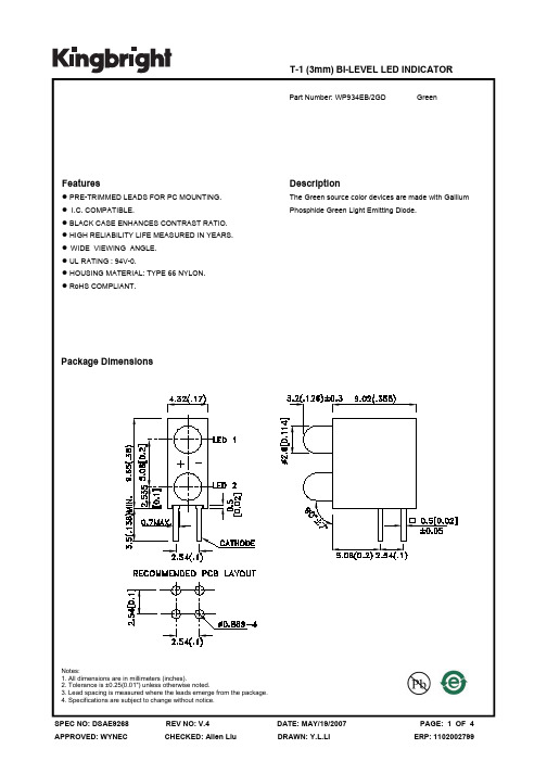
WP934EB/2GD
SPEC NO: DSAE9268 APPROVED: WYNEC
REV NO: V.4 CHECKED: Allen Liu
DATE: MAY/19/2007 DRAWN: Y.L.LI
PAGE: 4 OF 4 ERP: 1102002799
Green
WP934EB/2GD
SPEC NO: DSAE9268 APPROVED: WYNEC
REV NO: V.4 CHECKED: Allen Liu
DATE: MAY/19/2007 DRAWN: Y.L.LI
PAGE: 3 OF 4 ERP: 1102002799
元器件交易网
Notes: 1.Wavelength: +/-1nm. 2. Forward Voltage: +/-0.1V.
Absolute Maximum Ratings at TA=25°C
Parameter Power dissipation DC Forward Current Peak Forward Current [1] Reverse Voltage Operating/Storage Temperature Lead Solder Temperature [2] Lead Solder Temperature [3]
Electrical / Optical Characteristics at TA=25°C
Symbol λpeak λD [1] Δλ1/2 C VF [2] IR Parameter Peak Wavelength Dominant Wavelength Spectral Line Half-width Capacitance Forward Voltage Reverse Current Device Green Green Green Green Green Green Typ. 565 568 30 15 2.2 2.5 10 Max. Units nm nm nm pF V uA Test Conditions IF=20mA IF=20mA IF=20mA VF=0V;f=1MHz IF=20mA VR = 5V
柿饼 M3 模块硬件手册说明书

柿饼M3模块硬件手册1.概要信息1.1产品简介柿饼M3是上海睿赛德电子科技有限公司基于柿饼UI开发的一款显示屏板卡,用于提供IoT、智能家居、消费电子等领域的屏幕开发解决方案。
作为柿饼派的升级版本,柿饼M3尺寸小巧,功能强悍,支持丰富的外设通讯接口,可外接传感器或其他主控单元,支持丰富的网络协议和音视频播放,此外,柿饼M3支持FOTA功能,便于远程维护升级。
1.2基本参数●主控:RT1806高性能32位处理器●内置SDRAM:32MB●板载Flash:16MB●支持RGB666接口,支持常见的480*272,800*480,1024*600分辨率●支持UART、SPI、SDIO、IIC通信接口●支持USB-HOST功能可接移动4G模块或U盘●支持音视频播放●支持硬件JPEG解码●支持丰富的网络协议(MQTT、HTTP、HTTPS、WebSocket、TCP)●搭配柿饼UI,界面开发便捷,控件丰富(支持多种常用控件、可支持自定义控件)支持小程序多APP应用●支持FOTA安全升级机制2.模块典型应用框图图示为模块典型应用框图,详细参考电路见参考原理图资料。
3.规格参数模块相关规格参数如下:主要参数最小值典型值最大值单位工作温度-202570℃储存温度-302580℃工作湿度10%60%90%RH供电电压 4.5 5.0 5.5V供电电流90100120mAI/O支持电压 3.0 3.3 3.6VCodec支持电压 2.5 3.8 3.1VUSB支持电压 3.0 3.3 3.6V通信电平 3.3V 静电防护(默认)2(接触)24(空气)KV推荐回流温度:4.尺寸与引脚定义4.1尺寸大小项目参数外形尺寸27mm(长)*27mm(宽)*3.5mm(高)焊盘中心间距 1.27mm焊盘距板边距离 2.7mm注:详细参数见封装资料。
4.2引脚定义图4.3默认引脚定义PIN引脚Symbol符号说明Remark备注1,2,49-64LCD_D22,LCD_D23,LCD_D2-LCD_D21RGB数据接口默认RGB666,详情见示意图3LCD_CLK LCD屏时钟线4LCD_DE LCD屏片选脚5LCD_HSYNC RGB帧同步信号6LCD_VSYNC RGB场同步信号7,8VCC_5V电源供电4.5V-5.5V9,10GND电源地11SDA IIC数据线12SCL IIC时钟线13SD_DETC SD卡使能接口14SPK_SHDN音频使能接口(低有效)15,16U2_RX,U2_TX UART2串口信号输出、输入该串口为控制台,默认参数为1152008N117PWM1LCD背光调节接口18PE5WiFi初始化引脚不使用WiFi功能时,可做通用IO使用19PE4WiFi复位引脚同上20TP_INT/PE3触摸IC初始化引脚不使用触摸功能时,可做通用IO使用21TP_RST/PE2触摸IC复位引脚同上22,23LCD_D0/U0_RX,LCD_D1/U0_TX LCD的D0,D1引脚该串口为预留串口,默认参数为1152008N124,25SDIO_D2,SDIO_D3SD卡的SDIO数据D2,D3引脚26SDIO_CMD SDIO的命令引脚27SDIO_CLK SDIO的时钟引脚28,29SDIO_D0,SDIO_D1SD卡的SDIO数据D0,D1引脚30SPI_MISO/PA3默认为WiFi的SPI引脚不使用WiFi功能时,可做通用IO或SPI使用31SPI_CLK/PA2同上32SPI_MOSI/PA1同上33SPI_CS0/PA0同上34,35USB_DM,USB_DP USB数据线36RESET CPU复位引脚37TV_OUT38,39TV_IN1,TV_IN040LRADC ADC-Key带ADC功能的按键,6位分辨率41FMINL42FMINR43LINEIN44MICIN45,46HPR,HPL音频右/左声道输出47,48HPCOM_FB,HPCOM免责声明上海睿赛德电子科技有限公司随附提供的文档资料旨在提供给您(本公司的客户)使用,仅限于且只能在本公司销售或提供服务的产品上使用。
莫尼森 3W宽电压隔离稳压DC-DC转换器 WRA_ZP-3WR2 WRB_ZP-3WR2系列说明书

PowerPax UK Ltd3W,wide input isolated & regulated DC-DC converterPatent Protection RoHSFEATURES● Wide range of input voltage (2:1) ● DIP package● Efficiency up to 86% ● 1.5KVDC isolation● Short circuit protection(automatic recovery) ●Operating temperature range:-40°C ~ +85°C ● Meet CISPR22/EN55022 CLASS A ● Meet EN60950The WRA_ZP-3WR2 & WRB_ZP-3WR2 Series are specially designed for applications where a wide range input voltage power supplies are isolated from the input power supply in a distributed power supply system on a circuit board. For these DC-DC converters, you can reduce the failure points of design, and save the manpower, material and time cost in developing micro power supply, and also ensure better quality, stability, safety protection, and reliability for the end products.These products apply to where: 1) Input voltage range ≤2:1;2) 1.5KVDC input and output isolation;3) Output regulated and low ripple noise is required.In circuits such as industrial control, electric power, communication system power supply, etc.Selection GuidePart No.Input V oltage (VDC) OutputEfficiency (%,Typ.) @ Full LoadMax. CapacitiveLoad ② (µF)certificationNominal (Range)Max.①Output V oltage(VDC)Output Current (mA)(Max./Min.)WRA0505ZP-3WR2 5 (4.5-9)11±5 ±300/±15 76 2200 --WRA0512ZP-3WR2 ±12±125/±6 78 1800 WRA0515ZP-3WR2 ±15 ±100/±5 78 1000 WRB0505ZP-3WR2 5 600/30 74 4700 WRB0512ZP-3WR2 12 250/12 77 2700 WRB0515ZP-3WR2 15 200/10 77 2200 WRA1205ZP-3WR2 12 (9-18)20±5 ±300/±15 81 2200 WRA1209ZP-3WR2 ±9 ±166/±8 84 2000 WRA1212ZP-3WR2 ±12 ±125/±6 84 1800 WRA1215ZP-3WR2 ±15 ±100/±5 85 1000 WRB1203ZP-3WR2 3.3 909/46 74 4700 WRB1205ZP-3WR2 5 600/30 81 4700 WRB1212ZP-3WR2 12 250/12 83 2700 WRB1215ZP-3WR2 15 200/10 82 2200 WRB1224ZP-3WR2 24 125/6 83 1800 WRA2405ZP-3WR2 24 (18-36)40±5 ±300/±15 82 2200 WRA2412ZP-3WR2 ±12 ±125/±6 84 1800 WRA2415ZP-3WR2 ±15 ±100/±5 84 1000 WRB2403ZP-3WR2 3.3 909/46 78 4700 WRB2405ZP-3WR2 5 600/30 81 4700 CE WRB2412ZP-3WR2 12 250/12 86 2700 --WRB2415ZP-3WR215200/10862200PowerPax UK LtdWRB2424ZP-3WR2 24 125/6 85 1800 WRA4805ZP-3WR2 48 (36-75)80±5 ±300/±15 82 2200 --WRA4812ZP-3WR2 ±12 ±125/±6 84 1800 WRA4815ZP-3WR2 ±15 ±100/±5 85 1000 WRB4803ZP-3WR2 3.3 909/46 76 4700 WRB4805ZP-3WR2 5 600/30 82 4700 WRB4812ZP-3WR2 12 250/12 86 2700 WRB4815ZP-3WR215200/10862200Note: ①. Absolute maximum rating without damage on the converter, but it isn't recommended; ②. For dual output converter, the given value is the same for each output.Input SpecificationsItemOperating ConditionsMin. Typ.Max.UnitInput Current (full load /no-load)5VDC input--811/40 --mA12VDC input 309/30 24VDC input 155/15 48VDC input 77/5 Reflected Ripple Current5VDC input-- 20 --12VDC input 30 24VDC input 30 48VDC input 30 Input impulse V oltage (1sec. max.)5VDC input-0.7 -- 12 VDC12VDC input -- 25 24VDC input -- 50 48VDC input -- 100 Starting V oltage5VDC input-- -- 4.5 12VDC input -- -- 9 24VDC input -- -- 18 48VDC input-- --36Input FilterPi filterOutput SpecificationsItemOperating ConditionsMin.Typ.Max.UnitOutput V oltage Accuracy-- ±1 ±3 %No load output V oltage Accuracy Input voltage range-- ±1.5 ±5 Balance of Output V oltage Dual output, balanced load-- ±0.5 ±1 Linear Regulation Full load, the input voltage is from low voltage to high voltage -- ±0.2 ±0.5 Load Regulation 5%-100% load -- ±0.2 ±0.5 Transient Recovery Time 25% load step change -- 0.5 2 ms Transient Response Deviation -- ±2 ±5 % Temperature Coefficient Full load -- ±0.02 ±0.03 %/°C Ripple&Noise* 20MHz bandwidth --5080mV p-pShort circuit Protection Input voltage rangeContinuous, self-recoveryNote: * Ripple and noise are measured by “parallel cable” method, please see DC-DC Converter Application Notes for specific operation.General SpecificationsItemOperating ConditionsMin. Typ. Max. Unit Insulation V oltageInput-output, with the test time of 1 minute and the leak current lower than 1mA1500----VDCPowerPax UK LtdInsulation Resistance Input-output, isolation voltage 500VDC 1000 -- -- M Ω Isolation Capacitance Input-output, 100KHz/0.1V-- 120 -- pFOperating Temperature Derating if the temperature is ≥85°C (see Fig. 1) -40 -- 85 ℃ Storage Temperature -55 -- 125 Casing Temperature Rise Ta=25℃-- 25 -- Hand Soldering Welding spot is 1.5mm away from the casing, 10 seconds -- -- 300 Storage HumidityNon-condensing-- -- 95 % Switching Frequency(PFM mode) 100% load, nominal input voltage -- 200 -- KHz MTBF MIL-HDBK-217F@25°C1000----K hoursPhysical SpecificationsCasing Material Aluminum Alloy Dimensions 32.00*20.00*10.80 mm Weight 14g(Typ.) CoolingFree convectionEMC SpecificationsEMIConducted emission CISPR22/EN55022 CLASS A(Bare component) CLASS B (see Fig.3-② for recommended circuit) Radiated emission CISPR22/EN55022 CLASS A(Bare component) CLASS B (see Fig.3-②for recommended circuit) EMSElectrostatic discharge IEC/EN61000-4-2 Contact ±4KV/ Air ±8KV perf. Criteria B Radiation immunity IEC/EN61000-4-3 10V/mperf. Criteria A EFTIEC/EN61000-4-4 ±2KV (see Fig.3-① for recommended circuit)perf. Criteria B Surge immunityIEC/EN61000-4-5 ±2KV (see Fig.3-①for recommended circuit) perf. Criteria B Conducted disturbance immunity IEC/EN61000-4-6 3 Vr.m.s perf. Criteria A Immunities of voltage dip, drop and short interruptionIEC/EN61000-4-29 0-70%perf. Criteria BProduct Characteristic Curve120100806040200-404085105120O u t p u t P o w e r P e r c e n t a g e (%)E nvironment T empe ra ture.()℃T e mpe ra ture De ra ting CurveS a fe Ope ra tion Are aFig. 1WR A2415ZP-3WR 25055 60 65 70 75 80 859095 100 18212427303336E f f i c i e n c y (%)Input Voltage(V)E fficiency Vs input Voltage(F ull L oad)WR A2415ZP-3WR 22030 40 50 6070 8090 100 102030405060708090100E f f i c i e n c y (%)Output Cur r ent Per centage(%)E fficiency Vs Output L oad(Vin=Vin-nominal)PowerPax UK LtdWR B2405ZP-3WR 25055 60 65 70 75 80 85 9095 100 18212427303336E f f i c i e n c y (%)Input Voltage(V)E fficiency Vs input Voltage (F ull L oad)WR B2405ZP-3WR 22030 40 50 6070 80 90100 102030405060708090100E f f i c i e n c y (%)Output Cur r ent Per centage(%)E fficiency Vs Output L oad(Vin=Vin-nominal)Design Reference1. Output load requirementsTo ensure that the module can work efficiently and reliably, its output min. load shall be no lower than 5% of the rated load when using, or the output ripple may increase rapidly. Ensure that the product working load must be higher than 5% of the rated load.2. Typical applicationAll the DC/DC converters of this series are tested according to the recommended circuit (see Fig. 2) before delivery.If it is required to further reduce input and output ripple, properly increase the input & output of additional capacitors Cin and Cout or select capacitors of low equivalent impedance provided that the capacitance is no larger than the max. capacitive load of the product.DC DCVinG ND+Vo0V C inC outVinG ND+Vo0VC inC outDC DC-VoC outDua lS ingleFig. 2Vin 5V&12V 24V&48V Cin 100µF10µF~47µFCout10µF3. EMC solution-recommended circuitVinGND+Vo-Vo (0V)DC /DCL O ADC 2L DM1②C 0MOVFUS E①C 1C Y VinGND+1C 3Fig. 3PowerPax UK LtdParameter description:Model Vin:5VVin:12VVin:24VVin:48VFUSE Slow blown fuses according to the actual input current selections of the clientsMOV -- S14K25 S14K35 S14K60 C0 1000µF 1000µF 330µF/50V330µF/100V C1 4.7µF/50V4.7µF/100VLDM1 12µHC2 4.7µF/50V4.7µF /100VC3 10µF CY11nF/2KVNote: ①.Part ① in the Fig. 3 is used for EMS test and part ② for EMI filtering, selected based on needs. ②.If there is no recommended parameters, the model no require the external component.EMC solution-recommended circuit PCB layoutDualSingleFig. 4Note: Note: the min. distance of the bonding pads between input grounding and output grounding shall be ≥ 2mm.4. Input currentWhen the electricity is provided by the unstable power supply, please make sure that the range of the output voltage fluctuation and the ripple voltage of the power supply do not exceed the indicators of the modules. Input current of power supply should afford the flash startup current of this kind of DC/DC module(see Fig. 5).Generally: Vin=5V Iave =1400mA Vin=12V Iave=620mA Vin=24V Iave=310mA Vin=48V Iave =150mAI n p u t C u r r e n t (A )Input Voltage (V)Input Voltage s copeIaveFig. 55. For more information please find DC-DC converter application notes on Dimensions and Recommended LayoutNote:1.Packing Information please refer to 'Product Packing Information'. Packing bag number: 58210008;2.The min. load shall be no lower than 5%, or the output ripple may increase rapidly; If the product is operated under the min. required load, the productperformance cannot be guaranteed to comply with all performance indexes in the Manual, but the reliability of the product will not be influenced;3.The unbalance degree of the recommended dual output module load: ≤ 5%; if the degree exceeds ±5%, then the product perf ormances cannot be guaranteedto comply with all the performance indicators in the manual, and please directly contact our technicians for specific information;4.The max. capacitive load should be tested within the input voltage range and under full load conditions;5.Unless otherwise specified, data in this datasheet should be tested under the conditions of Ta=25℃, humidity<75% when inputting nominal voltage andoutputting rated load;6.All index testing methods in this datasheet are based on our Company’s corporate standards;7.The performance indexes of the product models listed in this datasheet are as above, but some indexes of non-standard model products will exceed theabove-mentioned requirements, and please directly contact our technicians for specific information;8.We can provide product customization service;9.Specifications of this product are subject to changes without prior notice.PowerPax UK Ltd。
ASD934无线充智能测试设备用户手册说明书
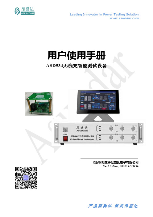
©版权归属于昂盛达电子有限公司Ver2.0 /Nov, 2020/ ASD934简介在某些情况下,用错误配置的市电电压为设备供电可能造成市电保险丝断开。
2.2 前面板介绍图 2.2:ASD934前面板图 2.3:ASD934后面板图 2.4.1:ASD934安卓触控屏图4.1.1 研发模式研发模式可以显示输入给无线充发射器的电压、电流、功率及D+、D-值,和显示无线充接收器提供给负载的电压、电流及功率值。
可同时或单独使用发射端或接收端,同时使用时可显示实时转换效率。
电源供电支持标准(无协议)、QC协议、PD协议三种方式,电压范围0~20V流所允许的上限值可设定。
负载受电可选择QI、Samsung、Apple和EPP标准,均支持5W、7.5W、10W四种功率选择,可测量电压范围0~20V,电流范围0~ 2A。
4.2自动模式无线充测试仪的自动模式主界面如图图4.2.1 自动模式每一项测试工序均可设置电源和负载两种功能,电源可选择标准、QC或PD协议,负载、Samsung、Apple和EPP标准。
可设置电源电压、最大输入电流、负载功率等多项参数,可设定发射和接收的参数范围作为判定指标。
保存好的工步条件可单步调试或复制粘贴、编辑、删除;自动测试按序号依次进行,可长按序号拖动进行自由排序;多道工序可保存为一个项目,项目数据可导出或导入至存储设备。
界面如图4.2.2所示。
图4.2.2 参数设置图5.1.1 开机启动界面点击操作终端右侧“设置”图标,弹出设置面板,如图5.1.2所示。
图5.1.2 设置面板“模式切换”图标即弹出模式切换窗口,可选择自动或研发两种工作模式,如图5.1.3所示。
图5.1.3 模式切换5.2研发模式图5.2.1 研发模式5.1章节的流程,正确连接测试线和无线充接收座并开机后,将发射端的测试线连接无线充发射器的电源输入接口,并将无线充接收座线圈位置正对于发射器线圈,应保持发射器线圈和接收器线圈位于同一中心轴上。
士兰微电子SD7530 LED照明高功率因数反激式PWM控制器说明书

高功率因数反激式PWM控制器
日光灯
产品规格分类
产品名称 封装形式 打印名称 材料 包装
无铅料管SD7530 DIP-8-300-2.54
SD7530
无铅料管
SD7530S
SD7530S SOP-8-225-1.27
无铅编带SD7530STR SOP-8-225-1.27
SD7530S
内部框图
40
OL -600/800
误差
放大器
比较器
SD7530说明书
电气参数 (除非特别指定,V
CC
=22V;C O=1nF;-25°C<T amb<125°C)
TEL 158********
SD7530说明书
TEL 158********
管脚描述
封装外形图
SD7530说明书
MOS电路操作注意事项:
静电在很多地方都会产生,采取下面的预防措施,可以有效防止MOS电路由于受静电放电影响而引起的损坏:
• 操作人员要通过防静电腕带接地。
• 设备外壳必须接地。
• 装配过程中使用的工具必须接地。
• 必须采用导体包装或抗静电材料包装或运输。
声明:
•士兰保留说明书的更改权,恕不另行通知!客户在下单前应获取最新版本资料,并验证相关信息是否完整和最新。
•任何半导体产品特定条件下都有一定的失效或发生故障的可能,买方有责任在使用Silan产品进行系统设计和整机制造时遵守安全标准并采取安全措施,以避免潜在失败风险可能造成人身伤害或财产损
失情况的发生!
•产品提升永无止境,我公司将竭诚为客户提供更优秀的产品!
TEL 158********。
L9341V中文资料
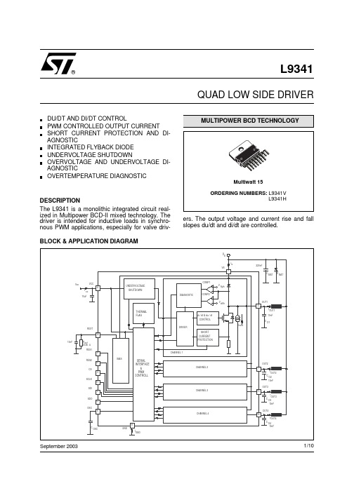
L9341QUAD LOW SIDE DRIVERDU/DT AND DI/DT CONTROLPWM CONTROLLED OUTPUT CURRENT SHORT CURRENT PROTECTION AND DI-AGNOSTICINTEGRATED FLYBACK DIODE UNDERVOLTAGE SHUTDOWNOVERVOLTAGE AND UNDERVOLTAGE DI-AGNOSTICOVERTEMPERATURE DIAGNOSTICDESCRIPTIONThe L9341 is a monolithic integrated circuit real-ized in Multipower BCD-II mixed technology. The driver is intended for inductive loads in synchro-nous PWM applications, especially for valve driv-ers. The output voltage and current rise and fall slopes du/dt and di/dt are controlled.September 2003®UNDERVOLTAGE SHUTDOWNDIAGNOSTICDRIVERSHORT CURRENT PROTECTIONCHANNEL 1CHANNEL 4CHANNEL 3CHANNEL 2VflythV offthCOMP1COMP2I OSCSDO SDI SCLK RES1SERIAL INTERFACE & PWM CONTROLLBIAS7115148613511RES2310912REXTCS 4OUT3OUT4GNDVSV sI I scc I OUT1I IOUT2OUT3I OUT4OSCC I GNDC BATD BATVccCO1C O2C C O3O4OUT2VCC2outsOUT1di / dt & du / dt CONTROLTHERMAL FLAG220nF10nF 10nF10nF 10nF10uFR ext 12.4k 10nFΩBLOCK & APPLICATION DIAGRAMMultiwatt 15ORDERING NUMBERS: L9341V L9341HMULTIPOWER BCD TECHNOLOGY1/10ABSOLUTE MAXIMUM RATINGSSymbol ParameterValue Unit V CC V CC Voltage Range-0.3 to 6V V S V S Voltage Range-0.3 to 24V V spmax VS Voltage Range for t ≤ 400ms -2 to 40V V st Schaffner Transient Pulses on V Ssee note 1VVin Input Voltage Range for SDI; SCLK;CS;RES1;RES2-0.3to V CC +0.3V outOutput Voltage Range for all Outputs:Negative Positive– 0.3intern. clamped to V SV V I outOutput Current for all Outputs:Negative Positive– 2+ 2A A for Transient with t < 10ms Negative Positive– 55A A Schaffner Transient Pulses on Output see note 2V ESDESD Voltage Capability (MIL 883 C)1500V THERMAL DATASymbol ParameterValue Unit R th j-case Thermal Resistance Junction to Case3°C/W R th j-amb Thermal Resistance Junction to Ambient mounted on PC Board 35°C/W T sdh Thermal Hysteresis 20°C T sdThermal DiagnosticT j > 150°CNotes:1. Schaffner transient specification: DIN 40839 test waveforms of the following type: 1, 2, 3a, 3b, 5 and 6. The pulses are applied to the application circuit according to fig. 3.2.The maximum output current results from the Schaffner pulses specified in note 1.PIN CONNECTION(Top view)ELECTRICAL CHARACTERISTICS (Unless otherwise specified: 8V ≤ V S≤ 24V; 4.7V ≤ V CC≤ 5.3V; –40 °C ≤ Tj ≤ 150°C; I O≤ 1A (note 3); I O≤ 1.5A; V sp = V S for t ≤ 400ms; V OUTP = V OUT for t ≤ 400ms;R ext = 12.4KΩ± 1%).Symbol Parameter Test Condition Min.Typ.Max.UnitI ccq V cc Quiescent Current All Outputs Off13mAI sq V s Quiescent Current All Outputs Off1425mAV ccu V cc Undervoltage Threshold See Note 434 4.7V V ccr V cc Range for RES1 and RES2Operation3VR on On Resistance I o = 1A T j = 125°CT j = 25°C 750450mΩmΩI o off Off State Output Current Outputs Off1.4V ≤ V o≤ V sV outp = V sp = 40V 112.5410mAmAV outf Output Voltage During Flyback I o = 1A Output OffT j = 25°C T j = 125°C V s +1.3V s +1.1VVI gndf Current to GND during Flyback(see note 5)I o = 1A Output OffV s = 24VV sp = 40V17204452mAmAI outr Reverse Leakage Current V sp - V o = 40V500µA V inH High Input Level of SCLK,SDI, CS, RES1, RES20.7*V cc V cc+0.3VV inL Low Input Level of SCLK,SDI, CS, RES1, RES2– 0.30.3*Vcc VV REShys Hysteresis of Reset InputsRES1, RES20.31VI inRESH Input Current on RES1,RES2RES i = H; -2V ≤ V sp≤ 8VRES i = H; 8V ≤ V sp≤ 40V – 1051010µAµAI in Input Current on SCLK,SDI,CS– 2V ≤ Vsp ≤ 40V– 1010µA V SDOH High Level SDO Output Voltage I SDO = -1mA -2V ≤ V sp≤ 40V0.9*V cc V cc V V SDOL Low Level SDO Output Voltage I SDO = 1mA -2V ≤ V sp≤ 40V00.4VI SDOZ SDO Tristate High-Z LeakageCurrent 0 ≤ V SDO≤ V cc– 2V ≤ V sp≤ 40V– 1010µAPWM duty PWM Duty Cycle1/1615/16 K f Frequency Accuracy Constant See Note 60.93*K fn K fn 1.07*K fnV flyth Flyback Diagnostic ComparatorThreshold 40 ≥ V sp≥ 8VV s≤ 8VV s – 11.5V s – 0.4VVV offth Off State DiagnosticComparator Threshold1.52VI outl Output Current Limitation Threshold see Note 7 1.5 2.5A t dpo Delay Time PWM Signal to Out.515µs S ov Output Voltage Rise and FallSlope | du/dt |(from 10 to 90% of V o) Fig. 2 1.010V/µsS oc Output Current Rise and FallSlope |di/dt|0.1 ≤ Io ≤ 1.5A(from 10 to 90% of I o)25125mA/µsNotes:3. The mean value is I o = 1T∫ I o(t) dtT;4. The outputs are switced off for Vcc ≤ Vccu. The logic is not reseted. For a reset, RES1 or RES2 must be used.5. This current is measured in the GND - terminal when one single output is in flyback and consists of the supply current added to the value of the output current source and the leakage current of the flyback diode. This leakage current is less than 1% of the nominal flyback current.6. The PWM frequency is defined by an external capacitor. The PWM oscillator frequency is: f pwm = f osc32with f osc =K fC osc⋅ 1A/V and k in = 15 ⋅ 10-6;the range is: 300Hz ≤ f pwm≤ 3000Hz. The OSC Pin can be alternatively driven by an external TTL / CMOS signal.7. For I out≥ I outl an internal comparator switches the corresponding output off for the current PWM cycle.15CLKPWM3PWM4PWM1PWM214131211109876543210Figure 1: Logic Diagram of PWM Generation.+12VI s I s12V01A 1A00du/dtdu/dt di/dtdi/dtdi/dtdi/dt 5%5%Internal PWM SignalI I Current through Flyback DiodeCurrent through Low Side Switch I GNDout V outt dpooutt dpofI fD DMOSDOUTV sDI fOutput Voltage V 20 mH510 nF220 nF Figure 2: Output Switching Diagram.220 nFD1Schaffner Generator4 x 10 nF-2V to 40 VVsGNDOUT1OUT2OUT3OUT44 x 1 nF+12V10 uFVCC+5VFigure 3: Test Circuit for Schaffner Pulses.INTERNAL CLOCKMSB 14131211321LSB MSB14131211321LSBSCLK SDI SDO CS SCLK SDI SDOt clcl t chclt cht clt clch t chcht sut ht dt clzt oht zch151415CS Figure 4: Synchronous Serial Interface Protocol.f clock Clock Frequencymin. DC max. 2MHzt ch Width of Clock Input High Puls min. 200ns t cl Widh of Clock Input Low Puls min. 200ns t cicl Clock Low Before CS Low min. 200ns t chcl Clock High After CS Low min. 200ns t clch Clock Low Before CS High min. 200ns t chch Clock High After CS High min. 200ns t ciz SDO Low-Z CS Low min. 0ns max. 400ns t zch SDO High-Z CS High max. 400nst su SDI Input Setup Time min. 80ns t h SDI Input Hold Timemin. 80nst d SDO Output Delay Time (C L = 50pF)max. 100nst ohSDO Output Hold Timemin. 0nsFigure 5: PWM Generation Function Table.Bit 3 - 0PWM1PWM2PWM3PWM4OUTPUT 000015/1615/1615/1615/16OFF 00011/1615/161/1615/16ON 00102/1614/162/1614/16ON 00113/1613/163/1613/16ON 01004/1612/164/1612/16ON 01015/1611/165/1611/16ON 01106/1610/166/1610/16ON 01117/169/167/169/16ON 10008/168/168/168/16ON 10019/167/169/167/16ON 101010/166/1610/166/16ON 101111/165/1611/165/16ON 110012/164/1612/164/16ON 110113/163/1613/163/16ON 111014/162/1614/162/16ON 111115/161/1615/161/16ONFigure 6:PWM Information From Microcontroller to QLSD.Bit. Contents0P10PWM Duty Cycle for Channel 1 / Bit 0: LSB1P11PWM Duty Cycle for Channel 1 / Bit 12P12PWM Duty Cycle for Channel 1 / Bit 23P13PWM Duty Cycle for Channel 1 / Bit 3 : MSB4P20PWM Duty Cycle for Channel 2 / Bit 0 : LSB5P21PWM Duty Cycle for Channel 2 / Bit 1 :6P22PWM Duty Cycle for Channel 2 / Bit 2 :7P23PWM Duty Cycle for Channel 2 / Bit 3 : MSB8P30PWM Duty Cycle for Channel 3 / Bit 0 : LSB9P31PWM Duty Cycle for Channel 3 / Bit 1 :10P32PWM Duty Cycle for Channel 3 / Bit 2 :11P33PWM Duty Cycle for Channel 3 / Bit 3 : MSB12P40PWM Duty Cycle for Channel 4 / Bit 0 : LSB13P41PWM Duty Cycle for Channel 4 / Bit 1:14P42PWM Duty Cycle for Channel 4 / Bit 2 :15P43PWM Duty Cycle for Channel 4 / Bit 3 : MSBBit Contents0F11COMP1 State at Positive Edge of PWM1 (0: V out1 > V flyth ; 1: V out1 < V flyth )1F12COMP2 State at Negative Edge of PWM1 (1: V out1 > V offth ; 0 : V out1 < V ofth )2F21COMP1 State at Positive Edge of PWM2 (0: V out2 > V flyth ; 1: V out2 < V flyth )3F22COMP2 State at Negative Edge of PWM2 (1: V out2 > V ofth ; 0 : V out2 < V ofth )4F31COMP1 State at Positive Edge of PWM3 (0: V out3 > V flyth ; 1: V out3 < V flyth )5F32COMP2 State at Negative Edge of PWM3 (1: V out3 > V offth ; 0 : V out3 < V ofth )6F41COMP1 State at Positive Edge of PWM4 (0: V out4 > V flyth ; 1: V out4 < V flyth )7F42COMP2 State at Negative Edge of PWM4 (1: V out4 > Voffth ; 0 : V out4 < V ofth )8RES1Logic State of RES1 Input (0: RES1 = L ; 1: RES1 = H)9RES2Logic State of RES2 Input (0: RES2 = L ; 1: RES2 = H)10TSDF Thermal Diagnostic Flag ( 0: Overtemperature ; 1:Normal )11C1Current at Negative Edge of PWM1 ( 0: I out > I outl ; 1: I out < I outl )12C2Current at Negative Edge of PWM2 ( 0: I out > I outl ; 1: I out < I outl )13C3Current at Negative Edge of PWM3 ( 0: I out > I outl ; 1: I out < I outl )14C4Current at Negative Edge of PWM4 ( 0: I out > I outl ; 1: I out < I outl )151Framing Information (always 1)Figure 7: Diagnostic Information from QLSD to Microcontroller.PWMV OUTPWM V OUT I Dt Ct VdPOPWMON t tminSample point COMP2Sample point COMP1dPOt t VPWMOFF t minSample point COMP2Sample point COMP1Fig.1Fig.2Figure 8.Fig. A Fig. B Note:For safty diagnostic take notice of the following conditions:t PWMON ≥ t dPOMAX + t C + t V (see Fig. A) t C = I D S OCMINt V =V outfmax S OVMINt PWMOFF ≥ t dPOMAX + t V (see Fig. B)FUNCTIONAL DESCRIPTIONThe U511 is a PWM quad low side driver for in-ductive loads. The duty cycle of the internal gen-erated PWM signal is set by a microcontroller via a serial interface for each output. An output slope limitation for both dv/dt and di /dt is implemented to reduce RFI. The PWM generation is realized avoiding a simultaneous output switching. As a result, di/dt becomes smaller. Integrated flyback diodes clamp the output voltage during the fly-back phase of the low side switches.The driver is protected against short circuit. An undervoltage shutdown circuit switches off all out-puts if V cc is less then V ccu. Below the shutdown voltage all outputs remain in off state regardless of the input state. After each malfunction which resets the driver, only the serial link interface can reactivate the normal function. In case of overcur-rent (I out = I out1), an internal comparator switches the output off. The overcurrent information can be read via the serial link for each driver separately at the negative edge of the corresponding PWM signal.The interface to the microcontroller is realized with a 16 bit synchronous serial peripheral inter-face (SPI). If CS is switched low, the serial link becomes active and SDO goes to low impedance. At the rising edge of the SCLK signal, one of the 16 bit of data stored in a shift register appear se-quencely at SDO. These data contain the 8 error flags, the status of thermal diagnostic flag and the external reset sources RES1, RES2 and the over-current flgs c1...c4. The last bit is framing infor-mation (see fig. 7). At each falling edge of SCLK, one of the 16 bits of data sent by the microcon-troller is transferred via the SDI input to the driver. These data contain the duty-cycle information for the internal PWM generation (4 times 4 bit).On the rising edge of CS the previously stored in-formation is transferred to the circuits. SDO be-come now high impedance and SDI is inactive. The serial interface of the QLSD is cascadable with the serial link interface of another QLSD, thus obtaining a 32 bit serial link information wich can control eight inductive loads. For a safety data transfer the takeover of data bits is only real-ized when the number of SCLK - clocks is n x 16 (n ≥ 1).The PWM duty cycle is set by 4 bit for each out-put independently via the serial link. If all four bits for an output are zero, the output is turned off, but the error diagnosis will work correctly (see fig. 5 and 6). The PWM frequency is defined by an ex-ternal capacitor on the OSC pin. Rext defines through the reference current the output current slope, the diagnostic current sink and the internal oscillator frequency (together with C osc).For error diagnosis the voltage on the output is measured during the on and off state of the par-ticular output driver. Upon the rising edge of the PWM signal (at this moment the power output is off and will be switched on) the status of COMP1 is stored into an internal latch. On the falling edge of the PWM signal ( the power output is on and will be switched off) the status of COMP2 is stored into another internal latch. This information can be read via the serial link for each output driver separately (see fig. 7).The thermal diagnostic switch the thermal flag to 0 in case of overtemperature T ≥T sd. It will be switched to 1 with the hysteresis T sdth in case of T < T sd - T sdh.To avoid male functions due to extensive noise or spikes at the supply pins V CC, V S and R ext mustbe blocked externally via capacitors.Multiwatt15 VDIM.mminchMIN.TYP.MAX.MIN.TYP.MAX.A 50.197B 2.650.104C 1.60.063D 10.039E 0.490.550.0190.022F 0.660.750.0260.030G 1.02 1.27 1.520.0400.0500.060G117.5317.7818.030.6900.7000.710H119.60.772H220.20.795L 21.922.222.50.8620.8740.886L121.722.122.50.8540.8700.886L217.6518.10.6950.713L317.2517.517.750.6790.6890.699L410.310.710.90.4060.4210.429L7 2.65 2.90.1040.114M 4.25 4.55 4.850.1670.1790.191M1 4.63 5.08 5.530.1820.2000.218S 1.9 2.60.0750.102S1 1.9 2.60.0750.102Dia13.653.850.1440.152OUTLINE AND MECHANICAL DATAInformation furnished is believed to be accurate and reliable. However, STMicroelectronics assumes no responsibility for the consequences of use of such information nor for any infringement of patents or other rights of third parties which may result from its use. No license is granted by implication or otherwise under any patent or patent rights of STMicroelectronics. Specifications mentioned in this publication are subject to change without notice. This publication supersedes and replaces all information previously supplied. STMicroelectronics products are not authorized for use as critical components in life support devices or systems without express written approval of STMicroelectronics.The ST logo is a registered trademark of STMicroelectronics.All other names are the property of their respective owners© 2003 STMicroelectronics - All rights reservedSTMicroelectronics GROUP OF COMPANIESAustralia – Belgium - Brazil - Canada - China – Czech Republic - Finland - France - Germany - Hong Kong - India - Israel - Italy - Japan -Malaysia - Malta - Morocco - Singapore - Spain - Sweden - Switzerland - United Kingdom - United States。
X9314WSM中文资料

The X9314 is a resistor array composed of 31 resistive elements. Between each element and at either end are tap points accessible to the wiper element. The position of the wiper element is controlled by the CS, U/D, and INC inputs. The position of the wiper can be stored in nonvolatile memory and then be recalled upon a subsequent power-up operation.
PIN CONFIGURATION
8-LEAD DIP/SOIC
INC U/D VH VSS
1
8
2
7
X9314
3
6
4
5
VCC CS
VL VW
VH VSS VW
VL
8-LEAD MSOP
1
8
2
7
X9314
3
6
4
5
U/D INC VCC CS
6427 ILL F02.2
夜間雲端無線網路攝影機 IC-3140W 產品說明说明书

IC-3140WH.264夜間雲端無線網路攝影機產品資訊1-1 包裝內容IC-3140W安裝指南CD電源變壓器 網路線 壁掛安裝組件1-2 前面板麥克風PIR 人體紅外線感應器LED 指示燈紅外線LED 燈可調焦鏡頭 光線感應器1-3 背板1-4 LED 指示燈MAC/Cloud ID 及Setup SSID LAN 埠12V DC 電源連接埠WPS/Reset 按鍵MicroSD 卡插槽喇叭1-5背板標籤貼紙本產品背面貼有著標籤貼紙,貼紙上印有MAC位址、Cloud ID及Setup SSID 等資訊。
為方便對照使用,本產品的Mac 位址與Cloud ID是一樣的。
Cloud ID是為了讓您可以遠端觀看本產品所拍攝的即時影像時使用。
硬體安裝壁掛安裝組件安裝本產品可站立擺放也可搭配附贈的基座做壁掛式安裝。
1.組裝壁掛基座方式如下圖示:2.將壁掛基座上的螺絲頭栓入本產品背板上的螺絲孔如您家中有三角架,您也可以將本產品安裝在其上使用攝影機本體安裝請按照下面的說明以確保您的攝影機已正確連接並安裝就緒。
1.請將電源變壓器連接至本產品背板下方的電源連接埠,並將插頭端插入電源插座。
2.請稍待本產品開機完成。
在開機過程中,機器本身會發出一些聲音,這是正常的現象,並且當它開機完成時,綠色的電源LED燈號會呈現慢速閃爍的狀態。
設定本產品須使用有線連網方式進行(請參照操作手冊說明)。
3.請使用您的手機或平板,依您其作業系統至Google Play或Apple AppStore搜尋〝EdiLife〞APP,然後下載並安裝。
4.iOS用戶請在啟動EdiLife之前,先前往您iPhone的Wi-Fi設定,並連接到您網路攝影機的SSID (EdiView.Setup **),接著請前往步驟7。
5.Android用戶請啟動EdiLife後,點擊視窗畫面右上方的+圖示(如下右圖示)。
6.Android用戶請自可用的無線裝置清單中選擇您的無線網路攝影機後,耐心稍待APP建立連線。
- 1、下载文档前请自行甄别文档内容的完整性,平台不提供额外的编辑、内容补充、找答案等附加服务。
- 2、"仅部分预览"的文档,不可在线预览部分如存在完整性等问题,可反馈申请退款(可完整预览的文档不适用该条件!)。
- 3、如文档侵犯您的权益,请联系客服反馈,我们会尽快为您处理(人工客服工作时间:9:00-18:30)。
Description
The High Efficiency Red source color devices are made with Gallium Arsenide Phosphide on Gallium Phosphide Orange Light Emitting Diode.
Package Dimensions
Notes: 1.Wavelength: +/-1nm. 2. Forward Voltage: +/-0.1V.
Absolute Maximum Ratings at TA=25°C
Parameter Power dissipation DC Forward Current Peak Forward Current [1] Reverse Voltage Operating/Storage Temperature Lead Solder Temperature [2] Lead Solder Temperature [3]
Part No. Dice Lens Type Iv (mcd) [2] @ 10mA Min. WP934RZ/3ID HIGH EFFICIENCY RED (GaAsP/GaP) RED DIFFUSED 8 Typ. 20 Viewing Angle [1] 2 θ 1/2 40°
Notes: 1. θ1/2 is the angle from optical centerline where the luminous intensity is 1/2 the optical centerline value. 2. Luminous intensity/ luminous Flux: +/-15%.
Units mW mA mA V
SPEC NO: DSAF1894 APPROVED: WYNEC
REV NO: V.2 CHECKED: Allen Liu
DATE: APR/13/2007 DRAWN: S.J.LIU
PAGE: 2 OF 4 ERP:1102003393
元器件交易网
元器件交易网
T-1 (3mm) TRI-LEVEL LED INDICATOR
Part Number: WP934RZ/3ID
HIGH EFFICIENCY RED
Features
TRI-LEVEL DESIGN. DIFFERENT COLOR COMBINATION AVAILABLE. BLACK CASE ENHANCES CONTRAST RATIO. HIGH RELIABILITY LIFE MEASURED IN YEARS. UL RATING : 94V-0. HOUSING MATERIAL: TYPE 66 NYLON. RoHS COMPLIANT.
SPEC NO: DSAF1894 APPROVED: WYNEC
REV NO: V.2 CHECKED: Allen Liu
DATE: APR/13/2007 DRAWN: S.J.LIU
PAGE: 1 OF 4 ERP:1102003393
元器件交易网
Selection Guide
PAGE: 4 OF 4 ERP:1102003393
High EfficiencPEC NO: DSAF1894 APPROVED: WYNEC
REV NO: V.2 CHECKED: Allen Liu
DATE: APR/13/2007 DRAWN: S.J.LIU
PAGE: 3 OF 4 ERP:1102003393
Notes: 1. 1/10 Duty Cycle, 0.1ms Pulse Width. 2. 2mm below package base. 3. 5mm below package base.
High Efficiency Red 75 30 160 5 -40°C To +85°C 260°C For 3 Seconds 260°C For 5 Seconds
Notes: 1. All dimensions are in millimeters (inches). 2. Tolerance is ±0.25(0.01") unless otherwise noted. 3. Lead spacing is measured where the leads emerge from the package. 4. Specifications are subject to change without notice.
Electrical / Optical Characteristics at TA=25°C
Symbol λpeak λD [1] Δλ1/2 C VF [2] IR Parameter Peak Wavelength Dominant Wavelength Spectral Line Half-width Capacitance Forward Voltage Reverse Current Device High Efficiency Red High Efficiency Red High Efficiency Red High Efficiency Red High Efficiency Red High Efficiency Red Typ. 627 625 45 15 2.0 2.5 10 Max. Units nm nm nm pF V uA Test Conditions IF=20mA IF=20mA IF=20mA VF=0V;f=1MHz IF=20mA VR = 5V
元器件交易网
PACKING & LABEL SPECIFICATIONS
WP934RZ/3ID
SPEC NO: DSAF1894 APPROVED: WYNEC
REV NO: V.2 CHECKED: Allen Liu
DATE: APR/13/2007 DRAWN: S.J.LIU