NHD-10032AZ-FSY-GBW, 规格书,Datasheet 资料
FDS9933A;中文规格书,Datasheet资料

D2D2D1D1TRADEMARKSACEx™CoolFET™CROSSVOLT™E 2CMOS TM FACT™FACT Quiet Series™FAST ®FASTr™GTO™HiSeC™The following are registered and unregistered trademarks Fairchild Semiconductor owns or is authorized to use and is not intended to be an exhaustive list of all such trademarks.LIFE SUPPORT POLICYFAIRCHILD’S PRODUCTS ARE NOT AUTHORIZED FOR USE AS CRITICAL COMPONENTS IN LIFE SUPPORTDEVICES OR SYSTEMS WITHOUT THE EXPRESS WRITTEN APPROV AL OF FAIRCHILD SEMICONDUCTOR CORPORATION.As used herein:1. Life support devices or systems are devices or systems which, (a) are intended for surgical implant intothe body, or (b) support or sustain life, or (c) whosefailure to perform when properly used in accordancewith instructions for use provided in the labeling, can be reasonably expected to result in significant injury to the user.2. A critical component is any component of a lifesupport device or system whose failure to perform can be reasonably expected to cause the failure of the life support device or system, or to affect its safety or effectiveness.PRODUCT STATUS DEFINITIONS Definition of Terms Datasheet Identification Product Status DefinitionAdvance InformationPreliminary No Identification Needed Obsolete This datasheet contains the design specifications for product development. Specifications may change in any manner without notice.This datasheet contains preliminary data, andsupplementary data will be published at a later date.Fairchild Semiconductor reserves the right to make changes at any time without notice in order to improve design.This datasheet contains final specifications. Fairchild Semiconductor reserves the right to make changes at any time without notice in order to improve design.This datasheet contains specifications on a product that has been discontinued by Fairchild semiconductor.The datasheet is printed for reference information only.Formative or In DesignFirst ProductionFull ProductionNot In ProductionDISCLAIMERFAIRCHILD SEMICONDUCTOR RESERVES THE RIGHT TO MAKE CHANGES WITHOUT FURTHER NOTICE TO ANY PRODUCTS HEREIN TO IMPROVE RELIABILITY , FUNCTION OR DESIGN. FAIRCHILD DOES NOT ASSUME ANY LIABILITY ARISING OUT OF THE APPLICATION OR USE OF ANY PRODUCT OR CIRCUIT DESCRIBED HEREIN; NEITHER DOES IT CONVEY ANY LICENSE UNDER ITS PATENT RIGHTS, NOR THE RIGHTS OF OTHERS.SyncFET™TinyLogic™UHC™VCX™ISOPLANAR™MICROWIRE™POP™PowerTrench QFET™QS™Quiet Series™SuperSOT™-3SuperSOT™-6SuperSOT™-8分销商库存信息: FAIRCHILDFDS9933A。
深蓝PDJY型配变监测计量终端说明书

PDJY 型配变监测计量终端使用说明书目录第一章概述1.1产品概述-------------------------------------------------------1 1.2执行标准-------------------------------------------------------1第二章主要技术指标及功能2.1技术参数-------------------------------------------------------3 2.2主要功能-------------------------------------------------------3 2.3扩展功能-------------------------------------------------------42.3.1变压器监测防盗功能------------------------------- --4第三章安装3.1外形及安装尺寸----------------------------------------------4 3.2通电检查-------------------------------------------------------5第四章运行及操作方法4.1终端面板及接线端子介绍----------------------------------54.1.1终端面板介绍------------------------------------------54.1.2终端接线端子介绍------------------------------------7 4.2终端与主站连接在线指示----------------------------------94.2.1终端在线指示------------------------------------------9 4.3操作菜单------------------------------------------------------94.3.1参数查询菜单-----------------------------------------104.3.2参数设置菜单-----------------------------------------124.3.3测量点数据菜单--------------------------------------134.3.4终端管理操作菜单-----------------------------------14 4.4参数设置-----------------------------------------------------144.4.1测量点的配置-----------------------------------------15第1章概述1.1产品概述PDJY型配变监测计量终端是我公司研发、生产的新技术产品,采用了一系列先进的微电子技术和最新的电子元器件、采用现代通信技术、支持并采用GPRS公用无线通信网络技术(支持多种远程通讯,如CDMA等);能够实现自动抄表、实时监测电网的三相电压、电流、功率因数、谐波等运行数据,可完成对整个配电线路的实时监测、数据分析、报表处理等综合管理,为低压配电线路的科学管理提供第一手可靠数据,是实现配电网络现代化的重要组成部分,是电力营销计量自动化系统中具有较高的实用价值的终端产品。
STWD100NPWY3F;STWD100NYWY3F;中文规格书,Datasheet资料

This is information on a product in full production.March 2012Doc ID 14134 Rev 61/25STWD100Watchdog timer circuitDatasheet − production dataFeatures■Current consumption 13 µA typ.■Available watchdog timeout periods are3.4 ms, 6.3 ms, 102 ms and 1.6 s ■Chip enable input■Open drain or push-pull WDO output ■Operating temperature range: –40 to +125 °C ■Package SOT23-5, SC70-5 (SOT323-5)Applications■Telecommunications ■Alarm systems ■Industrial equipment ■Networking ■Medical equipment■UPS (uninterruptible power supply)Contents STWD100Contents1Description . . . . . . . . . . . . . . . . . . . . . . . . . . . . . . . . . . . . . . . . . . . . . . . . . 52Operation . . . . . . . . . . . . . . . . . . . . . . . . . . . . . . . . . . . . . . . . . . . . . . . . . . 72.1Watchdog input (WDI) . . . . . . . . . . . . . . . . . . . . . . . . . . . . . . . . . . . . . . . . 72.2Watchdog output (WDO) . . . . . . . . . . . . . . . . . . . . . . . . . . . . . . . . . . . . . . 72.3Chip enable input (EN) . . . . . . . . . . . . . . . . . . . . . . . . . . . . . . . . . . . . . . . . 82.4Applications information . . . . . . . . . . . . . . . . . . . . . . . . . . . . . . . . . . . . . . . 8Interfacing to microprocessors with bidirectional reset pins. . . . . . . . . . . . . . . . . . . 8 3Watchdog timing . . . . . . . . . . . . . . . . . . . . . . . . . . . . . . . . . . . . . . . . . . . 10 4Maximum ratings . . . . . . . . . . . . . . . . . . . . . . . . . . . . . . . . . . . . . . . . . . . 15 5DC and AC parameters . . . . . . . . . . . . . . . . . . . . . . . . . . . . . . . . . . . . . . 16 6Package mechanical data . . . . . . . . . . . . . . . . . . . . . . . . . . . . . . . . . . . . 18 7Part numbering . . . . . . . . . . . . . . . . . . . . . . . . . . . . . . . . . . . . . . . . . . . . 22 8Package marking information . . . . . . . . . . . . . . . . . . . . . . . . . . . . . . . . 23 9Revision history . . . . . . . . . . . . . . . . . . . . . . . . . . . . . . . . . . . . . . . . . . . 242/25Doc ID 14134 Rev 6STWD100List of tables List of tablesTable 1.SOT23-5 and SC70-5 (SOT323-5) pin description. . . . . . . . . . . . . . . . . . . . . . . . . . . . . . . . 5 Table 2.Absolute maximum ratings. . . . . . . . . . . . . . . . . . . . . . . . . . . . . . . . . . . . . . . . . . . . . . . . . 15 Table 3.Operating and AC measurement conditions. . . . . . . . . . . . . . . . . . . . . . . . . . . . . . . . . . . . 16 Table 4.DC and AC characteristics . . . . . . . . . . . . . . . . . . . . . . . . . . . . . . . . . . . . . . . . . . . . . . . . . 17 Table 5.SOT23-5 - 5-lead small outline transistor package mechanical data . . . . . . . . . . . . . . . . . 19 Table 6.SC70 (SOT323-5) – 5-lead small outline transistor package mechanical data . . . . . . . . . 21 Table 7.Ordering information scheme. . . . . . . . . . . . . . . . . . . . . . . . . . . . . . . . . . . . . . . . . . . . . . . 22 Table 8.Device versions with marking descriptions. . . . . . . . . . . . . . . . . . . . . . . . . . . . . . . . . . . . . 23 Table 9.Document revision history . . . . . . . . . . . . . . . . . . . . . . . . . . . . . . . . . . . . . . . . . . . . . . . . . 24Doc ID 14134 Rev 63/25List of figures STWD100 List of figuresFigure 1.SOT23-5 and SC70-5 (SOT323-5) package connections . . . . . . . . . . . . . . . . . . . . . . . . . . 5 Figure 2.Logic diagram. . . . . . . . . . . . . . . . . . . . . . . . . . . . . . . . . . . . . . . . . . . . . . . . . . . . . . . . . . . . 6 Figure 3.Block diagram. . . . . . . . . . . . . . . . . . . . . . . . . . . . . . . . . . . . . . . . . . . . . . . . . . . . . . . . . . . . 6 Figure 4.Open drain WDO output connection. . . . . . . . . . . . . . . . . . . . . . . . . . . . . . . . . . . . . . . . . . . 8 Figure 5.Interfacing to microprocessors with bidirectional reset I/O. . . . . . . . . . . . . . . . . . . . . . . . . . 9 Figure 6.Power-up . . . . . . . . . . . . . . . . . . . . . . . . . . . . . . . . . . . . . . . . . . . . . . . . . . . . . . . . . . . . . . 10 Figure 7.Normal triggering . . . . . . . . . . . . . . . . . . . . . . . . . . . . . . . . . . . . . . . . . . . . . . . . . . . . . . . . 11 Figure 8.Timeout without re-trigger. . . . . . . . . . . . . . . . . . . . . . . . . . . . . . . . . . . . . . . . . . . . . . . . . . 12 Figure 9.Trigger after timeout. . . . . . . . . . . . . . . . . . . . . . . . . . . . . . . . . . . . . . . . . . . . . . . . . . . . . . 13 Figure 10.Enable pin, EN, triggering. . . . . . . . . . . . . . . . . . . . . . . . . . . . . . . . . . . . . . . . . . . . . . . . . . 14 Figure 11.SOT23-5 - 5-lead small outline transistor package outline. . . . . . . . . . . . . . . . . . . . . . . . . 18 Figure 12.SC70 (SOT323-5) - 5-lead small outline transistor package outline. . . . . . . . . . . . . . . . . . 20 4/25Doc ID 14134 Rev 6STWD100Description 1 DescriptionThe STWD100 watchdog timer circuits are self-contained devices which prevent systemfailures that are caused by certain types of hardware errors (non-responding peripherals,bus contention, etc.) or software errors (bad code jump, code stuck in loop, etc.).The STWD100 watchdog timer has an input, WDI, and an output, WDO. The input is used toclear the internal watchdog timer periodically within the specified timeout period, t wd. Whilethe system is operating correctly, it periodically toggles the watchdog input, WDI. If thesystem fails, the watchdog timer is not reset, a system alert is generated and the watchdogoutput, WDO, is asserted.The STWD100 circuit also has an enable pin, EN, which can enable or disable the watchdogfunctionality. The EN pin is connected to the internal pull-down resistor. The device isenabled if the EN pin is left floating.Figure 1.SOT23-5 and SC70-5 (SOT323-5) package connectionsTable 1.SOT23-5 and SC70-5 (SOT323-5) pin descriptionPin number Name Description1WDO Watchdog output2GND Ground3EN Enable pin4WDI Watchdog input5V CC Supply voltageDoc ID 14134 Rev 65/25Description STWD100 Figure 2.Logic diagramNote:WDO output is available in open drain or push-pull configuration.Figure 3.Block diagramNote:Positive pulse on enable pin EN longer than 1 µs resets the watchdog timer.6/25Doc ID 14134 Rev 6STWD100OperationDoc ID 14134 Rev 67/252 OperationThe STWD100 device is used to detect an out-of-control MCU. The user has to ensure watchdog reset within the watchdog timeout period, otherwise the watchdog output is asserted and MCU is restarted. The STWD100 can be also enabled or disabled by the chip enable pin.2.1 Watchdog input (WDI)The WDI input has to be toggled within the watchdog timeout period, t WD , otherwise thewatchdog output, WDO, is asserted. The internal watchdog timer, which counts the t WD period, is cleared either:1.by a transition on watchdog output, WDO (see Figure 8) or 2. by a pulse on enable pin, EN (see Figure 10) or3.by toggling WDI input (low-to-high on all versions and high-to-low on STWD100xW, STWD100xX and STWD100xY only).The pulses on WDI input with a duration of at least 1 µs are detected and glitches shorter than 100 ns are ignored.If WDI is permanently tied high or low and EN is tied low, the WDO toggles every 3.4 ms (t WD ) on STWD100xP and every t WD and t PW on STWD100xW, STWD100xX and STWD100xY (see Figure 8).2.2 Watchdog output (WDO)When the V CC exceeds the timer startup voltage V ST ART after power-up, the internalwatchdog timer starts counting. If the timer is not cleared within the t WD , the WDO will go low (see Figure 6).After exceeding the t WD , the WDO is asserted for t PW on STWD100xW, STWD100xX and STWD100xY regardless of possible WDI transitions (see Figure 9). On STWD100xP WDO is asserted for a minimum of 10 µs and a maximum of t WD after exceeding the t WD period (see Figure 8 and Figure 9).The STWD100 has an active low open drain or push-pull output. An external pull-up resistor connected to any supply voltage up to 6 V is required in case of open drain WDO output (see Figure 4). Select a resistor value large enough to register a logic low, and small enough to register a logic high while supplying all input current and leakage paths connected to the reset output line. A 10 k Ω pull-up resistor is sufficient in most applications.OperationSTWD1008/25Doc ID 14134 Rev 6Open drain WDO output connection2.3 Chip enable input (EN)All states mentioned in Section 2.1: Watchdog input (WDI) and Section 2.2: Watchdog output (WDO) are valid under the condition that EN is in logical low state.The behavior of EN is common to all versions (i.e. STWD100xP , STWD100xW, STWD100xX and STWD100xY).If the EN goes high after power-up in less than t WD from the moment that V CC exceeds the timer startup voltage, V ST ART , the WDO will stay high for the same time period as EN, plus t WD (see Figure 10).If the EN goes high anytime during normal operation, the WDO will go high as well, but the minimum possible WDO pulse width is 10 µs (see Figure 10).The pulses on the EN pin with a duration of at least 1 µs are detected and glitches shorter than 100 ns are ignored.2.4 Applications informationInterfacing to microprocessors with bidirectional reset pinsMicroprocessors with bidirectional reset pins can contend with the STWD100 watchdogoutput, WDO. For example, if the WDO output is driven high and the micro wants to pull it low, signal contention will result. To prevent this from occurring, connect a 4.7 k Ω resistor between the WDO output and the microprocessors reset I/O as in Figure 5.STWD100OperationDoc ID 14134 Rev 69/25Watchdog timing STWD10010/25Doc ID 14134 Rev 63 Watchdog timing分销商库存信息:STMSTWD100NPWY3F STWD100NYWY3F。
航嘉电源2013年产品手册
C:\Documents and
外观结构图:Settings\liyis\桌
C:\Documents and
线材接口图(仅供参考,以实物为准):Settings\liyis\桌
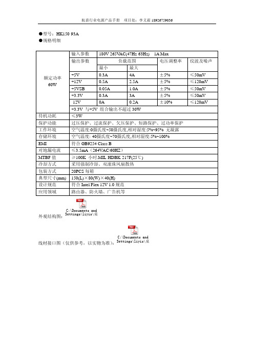
航嘉行业电源产品手册 项目处:李义霜 18926759036
●型号:HK250-93FP
●规格明细
输入参数 90V-265VAC(47Hz-63Hz) 3A Max
≤3W
过压保护、过流保护、欠压保护、短路保护、过功率保护
空气温度:0摄氏度~40摄氏度,相对湿度:5%~85% 无凝露
空气温度:-40摄氏度~70摄氏度,相对湿度:5%~95%
符合 GB9254 Class B
≤3.5mA(264VAC/60HZ)
≥100K 小时.MIL-HDBK-217F(25℃)
冷却方式
采用强制冷却、双滚珠风扇散热
包装方式
20PCS 每箱
典型尺寸(mm) 150(L)×80(W)×40(H)
设计规范
符合 Intel Flex 12V 1.0 规范
应用领域
路由器、防火墙、广告机等
纹波及噪声
≤50mV ≤120mV ≤50mV ≤50mV ≤120mV
C:\Documents and
≤3W
过压保护、过流保护、欠压保护、短路保护、过功率保护
空气温度:0摄氏度~50摄氏度,相对湿度:5%~95% 无凝露
空气温度:-40摄氏度~70摄氏度,相对湿度:5%~100%
符合 GB9254 Class B
≤3.5mA(264VAC/60HZ)
≥100K 小时.MIL-HDBK-217F(25℃)
C:\Documents and
5、整流二极管、雪崩整流二极管(13~60页)

特性曲线
图 1 典型 IF—VF 曲线
图 2 典型 IR—VR 曲线
17
2CZ152
产品结构:硅扩散台面型,玻璃钝化实体封装。 特 点:◆体积小,重量轻,单只重量约 0.2 克。
◆实体封装,密封性好,可靠性高。 ◆耐温度冲击。 质量等级及执行标准: ◆企军标 JP、JT 级
GJB33A-97 Q/FR20176-2005 ◆七专级“G”
VR=150V
IR12 VR=50V
型号
V
μA
max
max
2CZ136
1.1
10
型号与印章标志对照
极性:负极用色环表示 企标型号
2CZ136
μA max 1.0
印章标志
IR2 VR=150V TA=125℃
μA max 100
Z136
14
2CK75
永光电子有限公司 (国营第八七三厂)
产品结构:硅扩散台面型,环氧实体封装。 特 点:◆体积小,重量轻,单只重量约 0.1 克。
最大额定值
参数
VRWM
型号
V
IFa TA≤50℃
mA
IFSM 在 IF 下 tw=10ms
A
2CZ136
150
100
0.7
a 当 TA>50℃时,按 1mA/℃的速率线性地降额。
TOP
℃ -55~150
Tstg
℃ -55~150
电特性(TA=25℃± 3℃,除非另有规定)
特性
VF
IR11
在 IF 下
a 脉冲法:脉宽 300μs,占空比≤2%。
TA=150℃
规范值 最小 最大
—
10
—
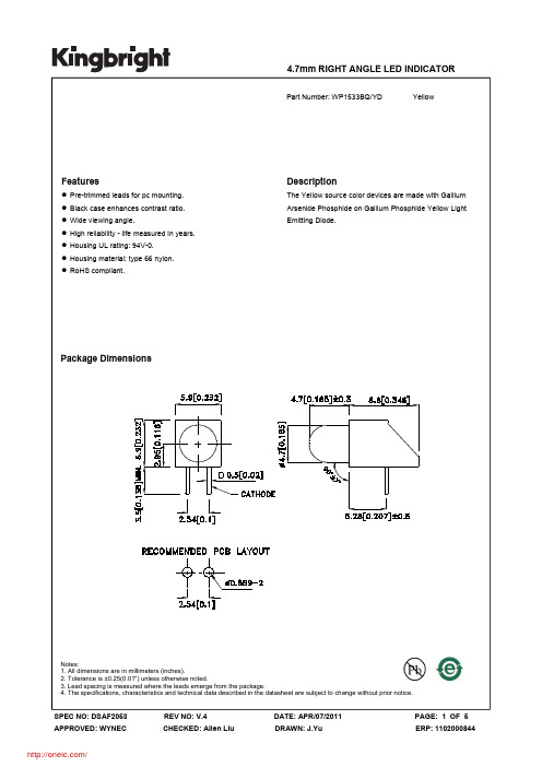
WP1533BQYD;中文规格书,Datasheet资料
分销商库存信息:
KINGBRIGHT WP1533BQ/YD
PACKING & LABEL SPECIFICATIONS
WP1533BQ/YD
SPEC NO: DSAF2053 APPROVED: WYNEC
REV NO: V.4 CHECKED: Allen Liu
DATE: APR/07/2011 DRAWN: J.Yu
PAGE: 4 OF 5 ERP: 1102000844
/
SPEC NO: DSAF2053 APPROVED: WYNEC
REV NO: V.4 CHECKED: Allen Liu
DATE: APR/07/2011 DRAWN: J.Yu
PAGE: 5 OF 5 ERP: 1102000844
/
SPEC NO: DSAF2053 APPROVED: WYNEC
REV NO: V.4 CHECKED: Allen Liu
DATE: APR/07/2011 DRAWN: J.Yu
PAGE: 1 OF 5 ERP: 1102000844
/
Selection Guide
Description
The Yellow source color devices are made with Gallium Arsenide Phosphide on Gallium Phosphide Yellow Light Emitting Diode.
Package Dimensions
Yellow
WP1533BQ/YD
SPEC NO: DSAF2053 APPROVED: WYNEC
REV NO: V.4 CHECKED: Allen Liu
沃伦森电气系列产品型号

沃伦森电气(WARENSEN)多年来一直专注于输配电系统无功补偿、滤波及电力电子设备的研发、生产和工程实施。
公司引入德国先进制造工艺和技术,坚持“积木式设计理念模块化成套产品”的产品战略,全心全意打造行业最具价值品牌!公司所生产的:WUAPF、WRS-APF、WMPF-12系列有源滤波装置主要应用于谐波污染严重的工况下;WRS-IC(R)、WRS-CRT(S)、WMT(S)C、WMXC-12、WMC-12、WMC-35系列无功补偿装置主要应用于电网等无功负荷波动较小的工况下;WRS-SVG、WDSVG、WIDSVG、WMSVC、WTSVC主要应用于无功负荷波动剧烈、电压闪变严重的工况下。
以上系列产品均可针对单独工程具体设计并提供项目策划书。
公司坚持“产品如人品质量是生命”的质量理念,保证产品卓越品质,并把“完美的产品是艺术品”作为产品制造工艺的唯一准则。
沃伦森电气(WARENSEN)在引入德国技术发展的同时,更注重人才与自主技术的储备,坚持与科研院所合作,定向培训、学术交流,联合建立研发基地,不断进行技术创新,提高产品先进性,保持行业领先水平。
一流的团队,一流的质量,一流的服务是我们的动力和源泉。
沃伦森电气(WARENSEN)不仅要做一个制造高品质产品的生产商,还要做一个用户满意,高效反应机制,不断创新的服务提供商。
互惠互利,与用户共赢,是我们永远的追求和目标。
电容器+电抗器WRS-CR7-10/400V WRS-MKP10/400-3 WRS-CK-10/400-3WRS-CR7-15/400V WRS-MKP15/400-3 WRS-CK-15/400-3WRS-CR7-20/400V WRS-MKP20/400-3 WRS-CK-20/400-3WRS-CR7-25/400V WRS-MKP25/400-3 WRS-CK-25/400-3WRS-CR7-30/400V WRS-MKP30/400-3 WRS-CK-30/400-3WRS-CR7-40/400V WRS-MKP40/400-3 WRS-CK-40/400-3WRS-CR14-10/400V WRS-MKP10/400-3 WRS-CK-10/400-3WRS-CR14-15/400V WRS-MKP15/400-3 WRS-CK-15/400-3WRS-CR14-20/400V WRS-MKP20/400-3 WRS-CK-20/400-3WRS-CR14-25/400V WRS-MKP25/400-3 WRS-CK-25/400-3WRS-CR14-30/400V WRS-MKP30/400-3 WRS-CK-30/400-3WRS-CR14-40/400V WRS-MKP40/400-3 WRS-CK-40/400-3电容电抗模块产品(晶闸管)WRS-CRT7-30/2-400VWRS-CRT7-30/2-400VWRS-CRT7-30/1-400VWRS-CRT7-30/2-400VWRS-CRT7-60/2-400VWRS-CRT7-60/2-400VWRS-CRT7-60/1-400VWRS-CRT7-60/2-400VWRS-CRT7-60/1-400VWRS-CRT7-60/2-400VWRS-CRT7-90/1-400VWRS-CRT7-60/1-400VWRS-CRT7-90/1-400VWRS-CRT7-60/2-400VWRS-CRT7-60/1-400VWRS-CRT7-90/1-400VWRS-CRT7-60/1-400VWRS-CRT7-90/1-400VWRS-CRT7-60/1-400VWRS-CRT7-90/1-400VWRS-CRT7-90/1-400VWRS-CRT14-30/2-400VWRS-CRT14-30/2-400VWRS-CRT14-30/1-400VWRS-CRT14-30/2-400VWRS-CRT14-60/2-400VWRS-CRT14-60/2-400VWRS-CRT14-60/1-400VWRS-CRT14-60/2-400VWRS-CRT14-60/1-400VWRS-CRT14-60/2-400VWRS-CRT14-90/1-400VWRS-CRT14-60/2-400VWRS-CRT14-60/1-400VWRS-CRT14-90/1-400VWRS-CRT14-60/2-400VWRS-CRT14-60/1-400VWRS-CRT14-90/1-400VWRS-CRT14-60/1-400VWRS-CRT14-90/1-400VWRS-CRT14-60/1-400VWRS-CRT14-90/1-400VWRS-CRT14-90/1-400V电容电抗模块产品(接触器)WRS-CRS7-30/2-400VWRS-CRS7-30/2-400VWRS-CRS7-30/1-400VWRS-CRS7-30/2-400VWRS-CRS7-60/2-400VWRS-CRS7-60/2-400VWRS-CRS7-60/1-400VWRS-CRS7-60/2-400VWRS-CRS7-60/1-400VWRS-CRS7-60/2-400VWRS-CRS7-60/2-400V WRS-CRS7-60/1-400V WRS-CRS7-90/1-400V WRS-CRS7-60/2-400V WRS-CRS7-60/1-400V WRS-CRS7-90/1-400V WRS-CRS7-60/1-400V WRS-CRS7-90/1-400V WRS-CRS7-60/1-400V WRS-CRS7-90/1-400V WRS-CRS7-90/1-400V WRS-CRS7-400V WRS-CRS14-30/2-400V WRS-CRS14-30/2-400V WRS-CRS14-30/1-400V WRS-CRS14-30/2-400V WRS-CRS14-60/2-400V WRS-CRS14-60/2-400V WRS-CRS14-60/1-400V WRS-CRS14-60/2-400V WRS-CRS14-60/1-400V WRS-CRS14-60/2-400V WRS-CRS14-90/1-400V WRS-CRS14-60/2-400V WRS-CRS14-60/1-400V WRS-CRS14-90/1-400V WRS-CRS14-60/2-400V WRS-CRS14-60/1-400V WRS-CRS14-90/1-400V WRS-CRS14-60/1-400V WRS-CRS14-90/1-400V WRS-CRS14-60/1-400V WRS-CRS14-90/1-400V WRS-CRS14-90/1-400V 智能电容器WRS-IC-450/10WRS-IC-450/15WRS-IC-450/20WRS-IC-450/25WRS-IC-450/30WRS-IC-450/40WRS-IC-450/50WRS-IC-450/60WRS-IC-450/70智能电容器(电抗器)WRS-ICR7-480/10WRS-ICR7-480/15WRS-ICR7-480/20WRS-ICR7-480/24WRS-ICR7-480/30WRS-ICR7-480/35WRS-ICR7-480/40WRS-ICR7-480/45WRS-APF模块产品WRS-APF25/400VWRS-APF35/400VWRS-APF50/400VWRS-APF60/400VWRS-APF75/400VWRS-APF100/400VWRS-SVG模块产品WRS-SVG50/400VWRS-SVG100/400V静止无功发生器WRS-SVG WDSVG-12/1000-N WDSVG-12/2000-N磁控式动态补偿滤波装置WMSVC-12/600-600-N WMSVC-12/1000-1000-N WMSVC-12/1200-1200-N WMSVC-12/600-600-W WMSVC-12/1000-1000-W WMSVC-12/1200-1200-W 高压无功补偿装置WMC-12/1000-3NWMC-12/1200-4NWMC-12/1600-4NWMC-12/2000-5NWMC-12/1000-3WWMC-12/1200-4WWMC-12/1600-4WWMC-12/2000-5W高压线路装置WMXC-6/50+100JWMXC-6/100+100J WMXC-6/200+100J WMXC-6/100+200JWMXC-6/100+100 WMXC-12/50+100J WMXC-12/100+100J WMXC-12/200+100J WMXC-12/100+200J WMXC-12/100+100低压有源滤波装置WUAPF-480/50-2N WUAPF-480/75-2N WUAPF-480/100-3N WUAPF-480/125-3N WUAPF-480/150-3N WUAPF-480/200-4N低压无功补偿装置WMTC-400/90-4N WMTC-400/120-3N WMTC-400/180-4N WMTC-400/240-4N WMTC-400/300-5N WMTC-400/360-6N WMTC-400/480-6N低压无源滤波装置WTSF400-100/3-N WTSF400-200/4-N WTSF400-300/5-N低压控制器WRS-DK-12TWRS-DK-21TWRS-DK-12SWRS-DK-21S高压控制器WRS-HK-700智能电容器控制器WRS-IK-200电容器综合保护单元WRS-HB-1000电能质量在线监测装置WRS-600S动态补偿调节开关WRS-TD1永磁式电容投切真空开关WRS-ZNT12/630-Y。
最新版安科瑞AZG智能配电柜AZX智能配电箱介绍说明书

1.4 型号说明
AZG -□-□
容量等级(A) :630、500、400、300、250、200、160、 100 安装方式:N 户内
A:安科瑞;ZG:智能配电柜
AZX -□-□
容量等级(A) :400、315、250、200、160、100、80、63、 40、32、25安装方式:源自 暗装 M 明装� � � �
1.6 技术参数
额定电压 Ue 额定电流 In 额定频率 分断能力 绝缘电压 Ui 防护等级 颜色 工作温度 贮存温度 相对湿度 AZG 技术参数 AC400V/230V 630A~100A 50Hz 15kA 660V IP54 RAL7035(可按客户要求定制) -10℃~55℃ -25℃~65℃ ≤95%,不凝露
电气参数
结构特性 环境条件
通讯协议
电气参数
结构特性
环境条件
通讯协议
海拔 ≤2000m 污染等级 III RS485接口, Modbus-RTU 协议(或 DL/T645规约) AZX 技术参数 额定电压 Ue AC400V/230V 额定电流 In 400A 至25A 额定频率 50Hz 分断能力 10kA 绝缘电压 Ui 400V 防护等级 IP54 颜色 RAL7035(可按客户要求定制) 工作温度 -10℃~55℃ 贮存温度 -25℃~65℃ 相对湿度 ≤95%,不凝露 海拔 ≤2000m 污染等级 III RS485接口, Modbus-RTU 协议(或 DL/T645规约)
AZX 箱体规格 外形尺寸 宽×高×深(mm) 400×600×180 400×600×180 500×700×200 600×800×250
10 11
315 400
700×850×250
- 1、下载文档前请自行甄别文档内容的完整性,平台不提供额外的编辑、内容补充、找答案等附加服务。
- 2、"仅部分预览"的文档,不可在线预览部分如存在完整性等问题,可反馈申请退款(可完整预览的文档不适用该条件!)。
- 3、如文档侵犯您的权益,请联系客服反馈,我们会尽快为您处理(人工客服工作时间:9:00-18:30)。
User’s GuideNHD-10032A Z-FSY-G BW LCM(Liquid Crystal Display Graphic Module)RoHS CompliantNHD- 10032- A Z- F-SY-G-B-W- Newhaven Display100 x 32pixel sVersion LineTransflectiveSide Yellow/Green LED B/LSTN- Gray6:00 ViewWide Temperature (-20 ~ +70c)For product support, contactNewhaven Display International, LLC2511 Technology Drive, #101Elgin, IL 60124Tel: (847) 844-8795 Fax: (847) 844-8796October 18, 2007CONTENTS1 Mechanical diagram2 Block diagram3 Features4 Mechanical specifications5 Absolute maximum ratings6 Description Of Terminals7 DC Electrical Characteristics8 Optical Characteristics9 Timing Characteristics10 Display commandNewhaven Display International, LLC Page 2 of 14NHD-10032AZ-FSY-GBW1Newhaven Display International, LLC Page 3 of 14FeaturesFull dot-matrix structure with 100dots x 32 dots 1/32 duty ,1/5 bias STN LCD, positiveReflective LCD, yellow green 6 o’clock viewing angle 8 bits parallel data input5Absolute Maximum RatingsItemSymbol Min MaxUnit Power Voltage V DD -V SS 0 7.0 Input VoltageV O V SS V DD VOperating Temperature Range V OP -20 +70Storage Temperature RangeT ST -30 +80Newhaven Display International, LLC Page 4 of 14Signal ground for LCM2VDDPower Supply V LCD adjustment4RSInputMPU Register select input“0”:Instruction register (when writing)Busy flag address counter (When reading) “1”: Data register (when writing & reading) 5 R/W Input MPU Read/write select signal “0” for writing, “1” for reading6 E1 Input MPU Chip enable active “L”, SEG (1~60)7 E2 InputMPUChip enable active “L”, SEG (61~120) 8 NCNot connected9 / 12 DB0-DB3 Input/output MPULow-order lines of data bus with 3-state, Bi-directional function for use in dataTransaction with the MPU. These lines are Not used when interfacing with a 4-bit Microprocessor.13 / 16 DB4-DB7 Input/output MPUHigh-order lines of data bus with 3-state, bi-directional function for use in dataTransactions with the MPU. DB7 may also be used to check the busy flag.8V OT A =254.55.5 V Supply currentI DD V DD =5.0V;T A =250.75 1.5 mA Input leakage current I LKG1.0V DDV“L” level input voltageV ILTwice initial value or lessNewhaven Display International, LLC Page 5 of 14, V DD =5.0VCr-302Response time(rise) T r120 150 msResponse time(fall) T r120 150 msFor STN Type Display Module (T a=250.25V)Item Symbol Condition Min. Typ. Max. Unit Viewing angle 2 -60-406Response time(rise) T r150 250 msResponse time(fall) T r150 250 ms10Newhaven Display International, LLC Page 6 of 14Itemsymbol ConditionsMin.Max.unit System cycle time t cyc8 ns Address setup time t aw8 ns Address hold time t ah8 ns Data setup time t ds8 ns Data hold time t dh8 ns Control pulse width t ccnsRD access timet cc8100020 10 8010 90 ns Output disable timet oh6 CL=100pf1060 ns Read ns Enable pulse width Writet ewnsNewhaven Display International, LLC Page 7 of 1411Newhaven Display International, LLC Page 8 of 14The command turns the display on and offD=1: display ON D=0: display OFFDisplay start line (C0H~DFH)This command specifies the line address shown if Figure 3 and indicates the display line that corresponds to COM0. the display area begins at the specified line address and continues the line address increment direction. This area having the number of lines of the specified display duty is displayed. If the line address is changed dynamically by this command the vertical smooth scrolling and paging can be used.A0 E (RD) R/W (/WR) D7 D6 D5 D4 D3 D2 D1 D00 1 0 1 1 0 A4 A3 A2 A1 A0This command loads the display start line register.A4 A3 A2 A1 A0 Line address0 0 0 0 0 00 0 0 0 1 1/ / / / / /1 1 1 1 1 1FSet page address (B8H~BBH)This command specifies the page address that corresponds to the low address of the display data RAM when it is accessed by the MPU. Any bit of the display data RAM can be accessed when its page address and column address are specified. The display status is not changed even when the page address is changed.A0 E (RD) R/W (/WR) D7 D6 D5 D4 D3 D2 D1 D00 1 0 1 0 1 1 1 0 A1 A0This command loads the page address register.A1 A0 Page0 0 00 1 11 0 21 1 3Newhaven Display International, LLC Page 9 of 14Set column address (00H~4FH)This command specifies a column address of the display data RAM. When the display data RAM is accessed by the MPU continuously, the column address is incremented by 1 each time it is accessed from the set address. Therefore, the MPU can access to data continuously. The column address stops to be incremented at address 80, and the page address is not changed continuously.A0 E (RD) R/W (/WR) D7 D6 D5 D4 D3 D2 D1 D00 1 0 0 A6 A5 A4 A3 A2 A1 A0This command loads the column address register.A6 A5 A4 A3 A2 A1 A0 Column address0 0 0 0 0 0 0 00 0 0 0 0 0 1 1/ / / / / / / /1 0 0 1 1 1 1 4FRead statusA0 E (RD) R/W (/WR) D7 D6 D5 D4 D3 D2 D1 D00 1 0 Busy ADC On/off Reset A3 A2 A1 A0 Reading the command I/O register (A0=0) yields system status information.The busy bit indicates whether the driver will accept a command or not.Busy=1: the driver is currently executing a command or is resetting. No new command will be accepted.Busy=0: the driver will accept a new command.The ADC bit indicates the way column addresses are assigned to segment drivers.ADC=1 Normal. Column address nsegment driver u.The ON/OFF bit indicates the current status of the display.It is the inverse of the polarity of the display ON/OFF command.ON/OFF=1: display offON/OFF=0: display onThe RESET bit indicates whether the driver is executing a hardware or software reset or if it is in normal operating mode.Reset=1: currently executing reset command.Reset=0: normal operationNewhaven Display International, LLC Page 10 of 14Write display dataA0 E (RD) R/W (/WR) D7 D6 D5 D4 D3 D2 D1 D01 1 0 Write dataWrites 8-bit of data into the display data RAM, at a location specified by the contents of the column address and page address registers and then increments the column address register by one.Read display dataA0 E (RD) R/W (/WR) D7 D6 D5 D4 D3 D2 D1 D01 0 1 Read dataReads 8-bit of data from the data I/O latch, updates the contents of the I/O latch with display data from the display data RAM location specified by the contents of the column address and page address registers and then increments the column address register.After loading a new address into the column address register one dummy read is required before valid data is obtained.Select ADC (A0H, A1H)A0 E (RD) R/W (/WR) D7 D6 D5 D4 D3 D2 D1 D00 1 0 1 0 1 0 0 0 0 DThis command selects the relationship between display data RAM column addresses and segment drivers.D=1: SEG0column address 00H,…(normal).This command is provided to reduce restrictions on the placement of driver ICs and routing of traces during printed circuit board design. See Figure 2 go a table of segments and column addresses for the two values of D.Static drive ON/OFF (A4H, A5H)A0 E (RD) R/W (/WR) D7 D6 D5 D4 D3 D2 D1 D00 1 0 1 0 1 0 0 1 0 D Forces display on and all common outputs to be selected.D=1:static drive onD=0:static drive offNewhaven Display International, LLC Page 11 of 14Select duty (A8H; A9H)A0 E (RD) R/W (/WR) D7 D6 D5 D4 D3 D2 D1 D00 1 0 1 0 1 0 1 0 0 DThis command sets the duty cycle of the LCD drive and is only valid for the SED1520F and SED1522F.it is invalid for the SED1521F, which performs passive operation. The duty cycle of the SED1521F is determined by the externally generated FR signal.SED1520 SED1522D=: 1/32 duty cycle 1/16 duty cycleD=: 1/16 duty cycle 1/8 duty cycleWhen using the SED1520F0A, SED1522F0A (having a built-in oscillator) and the SED1521F0A continuously, set the duty as follows:SED1521FOA1/32 1/32SED1520FOA1/16 1/161/116 1/32SED1522FOA1/8 1/16READ-MODIFY-WRITE (E0H)A0 E (RD) R/W (/WR) D7 D6 D5 D4 D3 D2 D1 D00 1 0 1 1 1 0 0 0 0 0This command defeats column address register auto-increment after data reads. The current contents of the column address register are saved. This mode remains active until an end command is repeated.Operation sequence during cursor displayWhen the end command is entered, the column address is returned to the one used during input of read-modify-write command. This function can reduce the load of MPU when data change is repeated at a specificDisplay area (such as cursor blinking).*Any command other than data read or write can be used in the read-modify-write mode. However, the column address set command cannot be used.Newhaven Display International, LLC Page 12 of 14END (EEH)A0 E (RD) R/W (/WR) D7 D6 D5 D4 D3 D2 D1 D00 1 0 1 1 1 0 1 1 1This command cancels read-modify-write mode and restores the contents of the column address register to their value prior to the receipt of the read-modify-write command.Newhaven Display International, LLC Page 13 of 14RESET (E2H)A0 E (RD) R/W (/WR) D7 D6 D5 D4 D3 D2 D1 D00 1 0 1 1 1 0 1 1 1 0This command clearsThe display start line register.And set page address register to 3 page.It does not affect the contents of the display data RAM.When the power supply is turned on, a Reset signal is entered in the RES pin. The Reset command cannot be used instead of this Reset signal.Newhaven Display International, LLC Page 14 of 14。