CAT24WC32KATE13D中文资料
EIZO FlexScan S2433W 彩色液晶显示器 说明书

2
有关此显示器的注意事项
本产品适用于制作文档、查看多媒体内容以及其它普通用途。 为配合在销售目标区域使用,本产品已经过专门调整。如果产品使用地并非销售目标区域,则本产品的工作性 能可能与规格说明不符。 本产品担保仅在此手册中所描述的用途范围之内有效。 本手册中所述规格仅适用于我们指定的电源线与信号线。 本产品可与我们制造或指定的备选产品配合使用。 由于显示器电子零件的性能需要约 30 分钟才能稳定,因此在电源开启之后,应调整显示器 30 分钟以上。 为了降低因长期使用而出现的发光度变化以及保持稳定的发光度,建议您以较低亮度使用显示器。 当显示器长期显示一个图像的情况下再次改变显示画面会出现残影。使用屏幕保护程序或计时器避免长时间显 示同样的图像。 建议定期清洁,以保持显示器外观清洁同时延长使用寿命。( 请参阅下一页上的“清洁”。) 液晶面板采用高精技术制造。但是,LCD 面板上可能会出现像素缺失或像素发亮,这不是故障。 有效像素百分比 :99.9994% 或更高。 液晶显示屏的背光灯有一定的使用寿命。当显示屏变暗或开始闪烁时,请与您的经销商联系。 切勿用力按压显示屏或外框边缘,否则可能会导致显示故障,如干扰图案等问题。如果持续受压,液晶显示屏 可能会性能下降或损坏。(若液晶显示屏上残留压痕,使显示器处于黑屏或白屏状态。此症状可能消失。) 切勿用铅笔或铅笔等尖锐物体刮擦或按压显示屏,否则可能会使显示屏受损。切勿尝试用纸巾擦拭液晶显示屏, 否则可能会留下擦痕。 如果将冷的显示器带入室内,或者室内温度快速升高,则显示器内部和外部可能会产生结露。在此情况下,请 勿开启显示器并等至结露消失,否则可能会损坏显示器。
FT24C16`FT24C08 资料完整版

F MDCo nf i de n t i al© 2012 Fremont Micro Devices Inc. DS24C04_08_16-A0--page1Two-Wire Serial EEPROM4K, 8K and 16K (8-bit wide)FEATURES❑Low voltage and low power operations:FT24C04A/08A/16A: V CC = 1.8V to 5.5V❑ Maximum Standby current < 1µA (typically 0.02µA and 0.06µA @ 1.8V and 5.5V respectively). ❑ 16 bytes page write mode.❑ Partial page write operation allowed.❑ Internally organized: 512 x 8 (4K), 1024 x 8 (8K), 2048 x 8 (16K). ❑ Standard 2-wire bi-directional serial interface. ❑ Schmitt trigger, filtered inputs for noise protection. ❑ Self-timed Write Cycle (5ms maximum).❑ 1 MHz (5V), 400 kHz (1.8V, 2.5V, 2.7V) Compatibility. ❑ Automatic erase before write operation.❑ Write protect pin for hardware data protection.❑ High reliability: typically 1, 000,000 cycles endurance. ❑ 100 years data retention.❑ Industrial temperature range (-40o C to 85o C).❑Standard 8-lead DIP/SOP/MSOP/TSSOP/DFN and 5-lead SOT-23/TSOT-23 Pb-free packages.DESCRIPTIONThe FT24C04A/08A/16A series are 4,096/8,192/16,384 bits of serial Electrical Erasable andProgrammable Read Only Memory, commonly known as EEPROM. They are organized as 512/1,024/2,048 words of 8 bits (1 byte) each. The devices are fabricated with proprietary advanced CMOS process for low power and low voltage applications. These devices are available in standard 8-lead DIP, 8-lead SOP, 8-lead TSSOP, 8-lead DFN, 8-lead MSOP, and 5-lead SOT-23/TSOT-23 packages. A standard 2-wire serial interface is used to address all read and write functions. Our extended V CC range (1.8V to 5.5V) devices enables wide spectrum of applications.PIN CONFIGURATIONPin Name Pin FunctionA2, A1, A0 Device Address Inputs SDA Serial Data Input / Open Drain Output SCL Serial Clock Input WP Write Protect NC No-ConnectF MDCo nf i de nt i a l© 2012 Fremont Micro Devices Inc. DS24C04_08_16-A0--page2All these packaging types come in conventional or Pb-free certified.VCC W P SCL SDAA2A1A0G 8L DIP 8L SOP8L TSSOP W P VCCG ND FT24C04A/08A/16A 5L SOT-23SCL 8L DFN8L M SOP 5L TSO T-23ABSOLUTE MAXIMUM RATINGSIndustrial operating temperature: -40℃ to 85℃ Storage temperature:-50℃ to 125℃Input voltage on any pin relative to ground: -0.3V to V CC + 0.3V Maximum voltage: 8VESD protection on all pins: >2000V* Stresses exceed those listed under “Absolute Maximum Rating” may cause permanent damage to thedevice. Functional operation of the device at conditions beyond those listed in the specification is not guaranteed. Prolonged exposure to extreme conditions may affect device reliability or functionality .F MDCo nf i de nt i a l© 2012 Fremont Micro Devices Inc. DS24C04_08_16-A0--page3PIN DESCRIPTIONS(A) SERIAL CLOCK (SCL)The rising edge of this SCL input is to latch data into the EEPROM device while the falling edge of this clock is to clock data out of the EEPROM device.(B) DEVICE / CHIP SELECT ADDRESSES (A2, A1, A0)These are the chip select input signals for the serial EEPROM devices. Typically, these signals are hardwired to either V IH or V IL . If left unconnected, they are internally recognized as V IL . FT24C04A has A0 pin as no-connect. FT24C08A has both A0 and A1 pins as no-connect. For FT24C16A, all device address pins (A0-A2) are no-connect.(C) SERIAL DATA LINE (SDA)SDA data line is a bi-directional signal for the serial devices. It is an open drain output signal and can bewired-OR with other open-drain output devices.(D) WRITE PROTECT (WP)The FT24C04A/08A/16A devices have a WP pin to protect the whole EEPROM array from programming. Programming operations are allowed if WP pin is left un-connected or input to V IL . Conversely all programming functions are disabled if WP pin is connected to V IH or V CC . Read operations is not affected by the WP pin’s input level.Table AF MDCo nf i de nt i al© 2012 Fremont Micro Devices Inc. DS24C04_08_16-A0--page4Device Chip Select/DeviceAddress Pins UsedNo-Connect Pins Max number of similardevices on the samebusFT24C04A A2, A1 A0 4FT24C08A A2, A1, A0 2 FT24C16A(None)A2, A1, A01MEMORY ORGANIZATIONThe FT24C04A/08A/16A devices have 32/64/128 pages respectively. Since each page has 16 bytes, random word addressing to FT24C04A/08A/16A will require 9/10/11 bits data word addresses respectively.DEVICE OPERATION(A) SERIAL CLOCK AND DATA TRANSITIONSThe SDA pin is typically pulled to high by an external resistor. Data is allowed to change only whenSerial clock SCL is at V IL . Any SDA signal transition may interpret as either a START or STOP condition as described below. (B) START CONDITIONWith SCL V IH , a SDA transition from high to low is interpreted as a START condition. All valid commands must begin with a START condition.F MDCo nf i de nt i al© 2012 Fremont Micro Devices Inc. DS24C04_08_16-A0--page5(C) STOP CONDITIONWith SCL V IH , a SDA transition from low to high is interpreted as a STOP condition. All valid read or write commands end with a STOP condition. The device goes into the STANDBY mode if it is after a read command. A STOP condition after page or byte write command will trigger the chip into the STANDBY mode after the self-timed internal programming finish. (D) ACKNOWLEDGEThe 2-wire protocol transmits address and data to and from the EEPROM in 8 bit words. The EEPROM acknowledges the data or address by outputting a "0" after receiving each word. The ACKNOWLEDGE signal occurs on the 9th serial clock after each word. (E) STANDBY MODEThe EEPROM goes into low power STANDBY mode after a fresh power up, after receiving a STOP bit in read mode, or after completing a self-time internal programming operation.Figure 1: Timing diagram for START and STOP conditionsFigure 2: Timing diagram for output ACKNOWLEDGESCLSDASTART ConditionSTOP ConditionData Data Valid TransitionSCLData inData out START ConditionACKF MDCo nf i de nt i a l© 2012 Fremont Micro Devices Inc. DS24C04_08_16-A0--page6DEVICE ADDRESSINGThe 2-wire serial bus protocol mandates an 8 bits device address word after a START bit condition to invoke valid read or write command. The first four most significant bits of the device address must be 1010, which is common to all serial EEPROM devices. The next three bits are device address bits. These three device address bits (5th , 6th and 7th ) are to match with the external chip select/address pin states. If a match is made, the EEPROM device outputs an ACKNOWLEDGE signal after the 8th read/write bit, otherwise the chip will go into STANDBY mode. However, matching may not be needed for some or all device address bits (5th , 6th and 7th ) as noted below. The last or 8th bit is a read/write command bit. If the 8th bit is at V IH then the chip goes into read mode. If a “0” is detected, the device enters programming mode.FT24C04A uses A2 (5th ) and A1 (6th ) device address bits. Only four FT24C04A devices can be wired-OR on the same 2-wire bus. Their corresponding chip select address pins A2 and A1 must be hard wired and coded from 00 (b) to 11 (b). Chip select address pin A0 is not used.FT24C08A uses only A2 (5th ) device address bit. Only two FT24C08A devices can be wired-OR on the same 2-wire bus. Their corresponding chip select address pin A2 must be hard-wired and coded from 0 (b) to 1 (b). Chip select address pins A1 and A0 are not used.FT24C16A does not use any device address bit. Only one FT24C16A device can be used on the on 2-wire bus. Chip Select address pins A2, A1, and A0 are not used.WRITE OPERATIONS(A) BYTE WRITEA byte write operation starts when a micro-controller sends a START bit condition, follows by a proper EEPROM device address and then a write command. If the device address bits match the chip select address, the EEPROM device will acknowledge at the 9th clock cycle. The micro-controller will then send the rest of the lower 8 bits word address. At the 18th cycle, the EEPROM will acknowledge the 8-bit address word. The micro-controller will then transmit the 8 bit data. Following an ACKNOWLDEGE signal from the EEPROM at the 27th clock cycle, the micro-controller will issue a STOP bit. After receiving the STOP bit, the EEPROM will go into a self-timed programming mode during which all external inputs will be disabled. After a programming time of T WC , the byte programming will finish and the EEPROM device will return to the STANDBY mode.(B) PAGE WRITEA page write is similar to a byte write with the exception that one to sixteen bytes can be programmed along the same page or memory row. All FT24C04A/08A/16A are organized to have 16 bytes per memory row or page.With the same write command as the byte write, the micro-controller does not issue a STOP bit aftersending the 1st byte data and receiving the ACKNOWLEDGE signal from the EEPROM on the 27th clock cycle. Instead it sends out a second 8-bit data word, with the EEPROM acknowledging at the 36th cycle. This data sending and EEPROM acknowledging cycle repeats until the micro-controller sends a STOP bit after the n 9th clock cycle. After which the EEPROM device will go into a self-timed partial or full page programming mode. After the page programming completes after a time of T WC , the devices will return to the STANDBY mode.F MDCo nf i de nt i a l© 2012 Fremont Micro Devices Inc. DS24C04_08_16-A0--page7The least significant 4 bits of the word address (column address) increments internally by one after receiving each data word. The rest of the word address bits (row address) do not change internally, but pointing to a specific memory row or page to be programmed. The first page write data word can be of any column address. Up to 16 data words can be loaded into a page. If more then 16 data words are loaded, the 17th data word will be loaded to the 1st data word column address. The 18th data word will be loaded to the 2nd data word column address and so on. In other word, data word address (column address) will “roll” over the previously loaded data. (C) ACKNOWLEDGE POLLINGACKNOWLEDGE polling may be used to poll the programming status during a self-timed internal programming. By issuing a valid read or write address command, the EEPROM will not acknowledge at the 9th clock cycle if the device is still in the self-timed programming mode. However, if the programming completes and the chip has returned to the STANDBY mode, the device will return a valid ACKNOWLEDGE signal at the 9th clock cycle.READ OPERATIONSThe read command is similar to the write command except the 8th read/write bit in address word is set to “1”. The three read operation modes are described as follows:(A) CURRENT ADDRESS READThe EEPROM internal address word counter maintains the last read or write address plus one if the power supply to the device has not been cut off. To initiate a current address read operation, the micro-controller issues a START bit and a valid device address word with the read/write bit (8th ) set to “1”. The EEPROM will response with an ACKNOWLEDGE signal on the 9th serial clock cycle. An 8-bit data word will then be serially clocked out. The internal address word counter will then automatically increase by one. For current address read the micro-controller will not issue an ACKNOWLEDGE signal on the 18th clock cycle. The micro-controller issues a valid STOP bit after the 18th clock cycle to terminate the read operation. The device then returns to STANDBY mode.(B) SEQUENTIAL READThe sequential read is very similar to current address read. The micro-controller issues a START bitand a valid device address word with read/write bit (8th ) set to “1”. The EEPROM will response with an ACKNOWLEDGE signal on the 9th serial clock cycle. An 8-bit data word will then be serially clocked out. Meanwhile the internally address word counter will then automatically increase by one. Unlike current address read, the micro-controller sends an ACKNOWLEDGE signal on the 18th clock cycle signaling the EEPROM device that it wants another byte of data. Upon receiving the ACKNOWLEDGE signal, the EEPROM will serially clocked out an 8-bit data word based on the incremented internal address counter. If the micro-controller needs another data, it sends out an ACKNOWLEDGE signal on the 27th clock cycle. Another 8-bit data word will then be serially clocked out. This sequential read continues as long as the micro-controller sends an ACKNOWLEDGE signal after receiving a new data word. When the internal address counter reaches its maximum valid address, it rolls over to the beginning of the memory array address. Similar to current address read, the micro-controller can terminate the sequential read by not acknowledging the last data word received, but sending a STOP bit afterwards instead.(C) RANDOM READRandom read is a two-steps process. The first step is to initialize the internal address counter with a target read address using a “dummy write” instruction. The second step is a current address read.To initialize the internal address counter with a target read address, the micro-controller issues a START bit first, follows by a valid device address with the read/write bit (8th ) set to “0”. The EEPROM will then acknowledge. The micro-controller will then send the address word. Again the EEPROM willacknowledge. Instead of sending a valid written data to the EEPROM, the micro-controller performs a current address readinstruction to read the data. Note that once a START bit is issued, the EEPROM will reset the internal programming process and continue to execute the new instruction - which is to read the current address.laitnedifnoCDMF© 2012 Fremont Micro Devices Inc. DS24C04_08_16-A0--page8F MDCo nf i de nt i al© 2012 Fremont Micro Devices Inc. DS24C04_08_16-A0--page9Figure 8: SCL and SDA Bus TimingAC CHARACTERISTICS1.8 V2.5-5.0 V Symbol ParameterMin Max MinMax Unit f SCLClock frequency, SCL 400 1000 kHz t LOW Clock pulse width low1.20.7µst HIGH Clock pulse width high0.4 0.3 µst I Noise suppression time (1) 180 120 ns t AAClock low to data out valid 0.30.90.20.7µs t BUF Time the bus must be free before a new transmission can start (1)1.3 0.5µs t HD.STA START hold time0.6 0.25 µs t SU.STA START set-up time 0.6 0.25 µs t HD.DAT Data in hold time 0 0 µs t SU.DAT Data in set-up time100100nst R Input rise time (1)0.3 0.3 µst F Input fall time (1) 300 100 nst SU.STO STOP set-up time 0.6 0.25 µs t DH Date out hold time 50 50 ns WRWrite cycle time55msEndurance(1)25o C, Page Mode, 3.3V1,000,000Write CyclesNotes: 1. This Parameter is expected by characterization but are not fully screened by test.2. AC Measurement conditions: R L (Connects to Vcc): 1.3K ΩInput Pulse Voltages: 0.3Vcc to 0.7VccInput and output timing reference Voltages: 0.5VccF MDCo nf i de nt i al© 2012 Fremont Micro Devices Inc. DS24C04_08_16-A0--page10DC CHARACTERISTICSSymbol Parameter Test ConditionsMin Typical Max Units V CC1 24C A supply V CC1.8 5.5 V I CC Supply read currentV CC @ 5.0V SCL = 400 kHz0.5 1.0 mA I CCSupply write current V CC @ 5.0V SCL = 400 kHz2.03.0 mA I SB1 Supply current V CC @ 1.8V, V IN = V CC or V SS 1.0 µA I SB2 Supply current V CC @ 2.5V, V IN = V CC or V SS 1.0 µA I SB3 Supply currentV CC @ 5.0V, V IN = V CC or V SS 0.06 1.0 µA I ILInput leakagecurrentV IN = V CC or V SS 3.0 µA I LOOutput leakagecurrentV IN = V CC or V SS3.0µAV IL Input low level -0.6 V CC x 0.3 V V IHInput high levelV CC x 0.7V CC +0.5 VV OL1 Output low level V CC @ 1.8V, I OL = 0.15 mA0.2 V V OL2 Output low level V CC @ 3.0V, I OL = 2.1 mA0.4VF MDCo nf i de nt i a l© 2012 Fremont Micro Devices Inc. DS24C04_08_16-A0--page11ORDERING INFORMATION:Density PackageTemperatureRangeVcc HSF Packaging Ordering CodeRoHSTube FT24C04A-UDR-BDIP8 -40℃-85℃ 1.8V-5.5VGreen Tube FT24C04A-UDG-B Tube FT24C04A-USR-B RoHSTape and Reel FT24C04A-USR-TTube FT24C04A-USG-B SOP8 -40℃-85℃ 1.8V-5.5VGreen Tape and Reel FT24C04A-USG-TTube FT24C04A-UMR-B RoHS Tape and Reel FT24C04A-UMR-TTube FT24C04A-UMG-B MSOP8 -40℃-85℃ 1.8V-5.5VGreen Tape and Reel FT24C04A-UMG-TTube FT24C04A-UTR-B RoHSTape and Reel FT24C04A-UTR-TTube FT24C04A-UTG-B TSSOP8 -40℃-85℃ 1.8V-5.5VGreen Tape and Reel FT24C04A-UTG-T RoHS Tape and Reel FT24C04A-ULR-T SOT23-5 -40℃-85℃ 1.8V-5.5VGreen Tape and Reel FT24C04A-ULG-T RoHS Tape and Reel FT24C04A-UPR-T TSOT23-5 -40℃-85℃ 1.8V-5.5V Green Tape and Reel FT24C04A-UPG-T RoHS Tape and Reel FT24C04A-UNR-T 4kbitsDFN8 -40℃-85℃ 1.8V-5.5V Green Tape and Reel FT24C04A-UNG-TRoHS Tube FT24C08A-UDR-B DIP8 -40℃-85℃ 1.8V-5.5VGreen Tube FT24C08A-UDG-B Tube FT24C08A-USR-B RoHSTape and Reel FT24C08A-USR-TTube FT24C08A-USG-B 8kbitsSOP8 -40℃-85℃ 1.8V-5.5VGreenTape and Reel FT24C08A-USG-TD: DIP8 S: SOP8 M: MSOP8 T: TSSOP8 L: SOT23-5 P: TSOT23-5 N: DFN8Packaging B: TubeT: Tape and Reel HSF R: RoHS G: GreenU:-40F MDCo nf i de nt i a l© 2012 Fremont Micro Devices Inc. DS24C04_08_16-A0--page12Density Package TemperatureRangeVcc HSF Packaging Ordering CodeTube FT24C08A-UMR-BRoHSTape and Reel FT24C08A-UMR-TTube FT24C08A-UMG-B MSOP8 -40℃-85℃ 1.8V-5.5VGreen Tape and Reel FT24C08A-UMG-TTube FT24C08A-UTR-B RoHSTape and Reel FT24C08A-UTR-TTube FT24C08A-UTG-B TSSOP8 -40℃-85℃ 1.8V-5.5VGreen Tape and Reel FT24C08A-UTG-T RoHSTape and Reel FT24C08A-ULR-T SOT23-5 -40℃-85℃ 1.8V-5.5V Green Tape and Reel FT24C08A-ULG-T RoHS Tape and Reel FT24C08A-UPR-T TSOT23-5 -40℃-85℃ 1.8V-5.5V Green Tape and Reel FT24C08A-UPG-T RoHS Tape and Reel FT24C08A-UNR-T 8kbitsDFN8 -40℃-85℃ 1.8V-5.5V Green Tape and Reel FT24C08A-UNG-TRoHS Tube FT24C16A-UDR-B DIP8 -40℃-85℃ 1.8V-5.5VGreen Tube FT24C16A-UDG-B Tube FT24C16A-USR-B RoHSTape and Reel FT24C16A-USR-TTube FT24C16A-USG-B SOP8 -40℃-85℃ 1.8V-5.5VGreen Tape and Reel FT24C16A-USG-TTube FT24C16A-UMR-B RoHSTape and Reel FT24C16A-UMR-TTube FT24C16A-UMG-B MSOP8 -40℃-85℃ 1.8V-5.5VGreen Tape and Reel FT24C16A-UMG-TTube FT24C16A-UTR-B RoHS Tape and Reel FT24C16A-UTR-TTube FT24C16A-UTG-B TSSOP8 -40℃-85℃ 1.8V-5.5VGreen Tape and Reel FT24C16A-UTG-T RoHSTape and Reel FT24C16A-ULR-T SOT23-5 -40℃-85℃ 1.8V-5.5V Green Tape and Reel FT24C16A-ULG-T RoHS Tape and Reel FT24C16A-UPR-T TSOT23-5 -40℃-85℃ 1.8V-5.5VGreen Tape and Reel FT24C16A-UPG-T RoHS Tape and Reel FT24C16A-UNR-T 16kbitsDFN8 -40℃-85℃ 1.8V-5.5VGreenTape and Reel FT24C16A-UNG-TF MDCo nf i de nt i al© 2012 Fremont Micro Devices Inc. DS24C04_08_16-A0--page13DIP8 PACKAGE OUTLINEDIMENSIONSDimensions In MillimetersDimensions In InchesSymbolMin Max Min MaxA 3.710 4.310 0.146 0.170 A1 0.510 0.020 A2 3.200 3.600 0.126 0.142B 0.380 0.570 0.015 0.022B1 1.524(BSC ) 0.060(BSC )C 0.204 0.360 0.008 0.014D 9.000 9.400 0.354 0.370E 6.200 6.600 0.244 0.260 E1 7.320 7.920 0.288 0.312 e 2.540 (BSC) 0.100(BSC ) L 3.000 3.600 0.118 0.142 E2 8.400 9.000 0.331 0.354F MDCo nf i de nt i al© 2012 Fremont Micro Devices Inc. DS24C04_08_16-A0--page14SOP8 PACKAGE OUTLINE DIMENSIONSDimensions In MillimetersDimensions In InchesSymbolMin Max Min MaxA 1.350 1.750 0.053 0.069A1 0.100 0.250 0.004 0.010A2 1.350 1.550 0.053 0.061 b 0.330 0.510 0.013 0.020 c 0.170 0.250 0.006 0.010D 4.700 5.100 0.185 0.200E 3.800 4.000 0.150 0.157 E1 5.800 6.200 0.228 0.244 e 1.270 (BSC)0.050 (BSC)L 0.400 1.270 0.016 0.050 θ 0° 8° 0° 8°F MDCo nf i de nt i al© 2012 Fremont Micro Devices Inc. DS24C04_08_16-A0--page15MSOP8 PACKAGE OUTLINE DIMENSIONSDimensions In MillimetersDimensions In InchesSymbolMin Max Min MaxA 0.820 1.100 0.320 0.043 A1 0.020 0.150 0.001 0.006 A2 0.750 0.950 0.030 0.037 b 0.250 0.380 0.010 0.015 c 0.090 0.230 0.004 0.009 D 2.900 3.100 0.114 0.122 e 0.65 (BSC) 0.026 (BSC) E 2.900 3.100 0.114 0.122 E1 4.750 5.050 0.187 0.199 L 0.400 0.800 0.016 0.031 θ 0° 6° 0° 6°F MDCo nf i de nt i al© 2012 Fremont Micro Devices Inc. DS24C04_08_16-A0--page16TSSOP8 PACKAGE OUTLINEDIMENSIONSDimensions In MillimetersDimensions In Inches SymbolMinMax Min Max D 2.900 3.100 0.114 0.122 E4.3004.5000.1690.177b 0.190 0.300 0.007 0.012c 0.090 0.200 0.004 0.008 E1 6.250 6.550 0.246 0.258 A 1.100 0.043 A2 0.800 1.000 0.031 0.039 A1 0.020 0.150 0.001 0.006e 0.65 (BSC) 0.026 (BSC) L 0.500 0.700 0.020 0.028H 0.25 (TYP) 0.01 (TYP)θ 1°7° 1° 7°F MDCo n f i de nt i a l© 2012 Fremont Micro Devices Inc. DS24C04_08_16-A0--page17SOT-23-5 PACKAGE OUTLINE DIMENSIONSDimensions In MillimetersDimensions In InchesSymbolMin Max Min MaxA 1.050 1.250 0.041 0.049A1 0.000 0.100 0.000 0.004 A2 1.050 1.150 0.041 0.045 b 0.300 0.500 0.012 0.020 c 0.100 0.200 0.004 0.008 D 2.820 3.020 0.111 0.119 E 1.500 1.700 0.059 0.067 E1 2.650 2.950 0.104 0.116 e 0.95 (BSC) 0.037 (BSC) e1 1.800 2.000 0.071 0.079 L 0.300 0.600 0.012 0.024 θ 0° 8° 0° 6°F MDCo nf i de nt i a l© 2012 Fremont Micro Devices Inc. DS24C04_08_16-A0--page18TSOT-23-5 PACKAGE OUTLINE DIMENSIONSDimensions In MillimetersDimensions In InchesSymbolMin Max Min MaxA 0.700 0.900 0.028 0.035A1 0.000 0.100 0.000 0.004 A2 0.700 0.800 0.028 0.031 b 0.350 0.500 0.014 0.020 c 0.080 0.200 0.003 0.008 D 2.820 3.020 0.111 0.119 E 1.600 1.700 0.063 0.067 E1 2.650 2.950 0.104 0.116 e 0.95 (BSC) 0.037 (BSC) e1 1.90 (BSC) 0.075 (BSC) L 0.300 0.600 0.012 0.024 θ 0° 8° 0° 8°F MDCo nf i de n t i al© 2012 Fremont Micro Devices Inc. DS24C04_08_16-A0--page19DFN8 PACKAGE OUTLINE DIMENSIONSDimensions In MillimetersSymbolMinNomMaxA 0.70 0.75 0.80A1 - 0.02 0.05 b 0.18 0.25 0.03 c 0.18 0.20 0.25 D 1.902.00 2.10D2 1.50REF e 0.50BSC Nd 1.50BSC E 2.90 3.00 3.10 E2 1.60REFL 0.30 0.40 0.50 h 0.20 0.25 0.30F MDCo nf i de n t i al© 2012 Fremont Micro Devices Inc. DS24C04_08_16-A0--page20Fremont Micro Devices (SZ) Limited* Information furnished is believed to be accurate and reliable. However, Fremont Micro Devices, Incorporated (BVI) assumes no responsibility for the consequences of use of such information or for any infringement of patents of other rights of third parties which may result from its use. No license is granted by implication orotherwise under any patent rights of Fremont Micro Devices, Incorporated (BVI). Specifications mentioned in this publication are subject to change without notice. This publication supersedes and replaces all information previously supplied. Fremont Micro Devices, Incorporated (BVI) products are not authorized for use as critical components in life support devices or systems without express written approval of Fremont Micro Devices, Incorporated (BVI). The FMD logo is a registered trademark of Fremont Micro Devices, Incorporated (BVI). All other names are the property of their respective owners.。
UPC3241TB-E3-A;UPC3241TB-A;UPC3241TB-EVAL-A;中文规格书,Datasheet资料

MMIC
MEDIUM
OUTPUT
POWER
PO (sat) (dBm) + 9.0 (0.9 GHz) + 8.5 (1.9 GHz) + 11.0 (0.9 GHz) + 8.0 (1.9 GHz) + 12.5 (0.9 GHz) + 11.0 (1.5 GHz) + 9.5 (0.9 GHz) + 9.0 (1.9 GHz) + 9.0 (2.4 GHz) + 11.0 (0.9 GHz) + 10.5 (1.9 GHz) + 10.0 (2.4 GHz) + 12.5 (1.0 GHz) + 10 (2.2 GHz)
This device exhibits low noise figure and high power gain characteristics. This IC is manufactured using our UHS0 (Ultra High Speed Process) bipolar process.
Parameter Supply Voltage Total Circuit Current Power Dissipation Operating Ambient Temperature Storage Temperature Input Power Symbol VCC ICC PD TA Tstg Pin TA = +25°C Conditions TA = +25°C, pin 4 and 6 TA = +25°C, pin 4 and 6 TA = +85C Note Ratings 4.0 55 270 40 to +85 55 to +150 10 Unit V mA mW °C °C dBm
VK3224中文手册
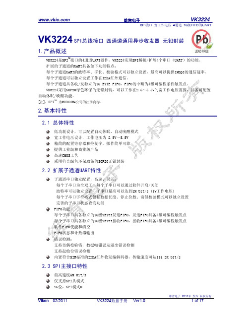
VK3224SPI总线接口四通道通用异步收发器无铅封装1.产品概述VK3224是SPI TM接口的4通道UART器件。
VK3224实现SPI桥接/扩展4个串口(UART)的功能。
扩展的子通道的UART具备如下功能特点:每个子通道UART的波特率、字长、校验格式可以独立设置,最高可以提供1Mbps的通信速率。
每个子通道可以独立设置工作在IrDA红外通信。
每个子通道具备收/发独立的16 BYTE FIFO,FIFO的中断为4级可编程条件触发点。
VK3224采用SOP20绿色环保的无铅封装,可以工作在2.5~5.5V的宽工作电压范围,具备可配置自动休眠/唤醒功能。
[注]:SPI TM为MOTOLORA公司的注册商标。
2.基本特性2.1 总体特性低功耗设计,可以配置自动休眠,自动唤醒模式精简的配置寄存器和控制字,操作简单可靠高速CMOS工艺子通道串口独立配置,高速、灵活:每个子串口为全双工,每个子串口可以通过软件开启/关闭波特率可以独立设置,子串口最高可以达到1M bit/s (5V工作电压)每个子串口字符格式包括数据长度、停止位数、奇偶校验模式可以独立设置完善的子串口状态查询功能FIFO功能:每个子串口具备独立的16级9Bits发送FIFO,发送FIFO具备4级可编程触发点每个子串口具备独立的16级9Bits接收FIFO,接收FIFO具备4级可编程触发点软件FIFO使能和清空FIFO状态和计数器输出内置符合SIR标准的IrDA红外收发编解码器,传输速度可达115.2K bit/s2.3 SPI主接口特性最高速度5M bit/s3.应用领域多串口服务器/多串口卡车载信息平台/车载GPS定位系统POS/税控POS/金融机具6.1封装图7.2 寄存器描述1:子串口1有中断7.2.5 SFOCR 子串口FIFO控制寄存器:(1001)位复位值功能描述类型W/R Bit7 – 6 00 TFTL1—0 发送FIFO触点控制:00=0bytes 01= 4bytes 10=8bytes 11=12bytes当接收FIFO的数据减少到该触发点时,提示主机可以继续向发送FIFO写入数据。
上海高通半导体有限公司GT24L24A2Y标准点阵中外文字库芯片说明书

GT24L24A2Y标准点阵中外文字库芯片V1.0_I_D2015-8版本修订记录目录1 概述 (4)1.1芯片特点 (4)1.2芯片内容 (5)字型样张 (7)1.32 操作指令 (14)2.1Instruction Parameter(指令参数) (14)Read Data Bytes(一般读取) (14)2.22.3Read Data Bytes at Higher Speed(快速读取点阵数据) (15)2.4 Write Enable(写使能) (16)2.5 Write Disable(写非能) (16)2.6 Page Program(页写入) (16)2.7 Sector Erase(扇区擦除) (17)2.8 深度睡眠模式指令(B9H) (17)2.9 唤醒深度睡眠模式指令(ABH) (17)3 引脚描述与电路连接 (18)3.1引脚配置 (18)3.2 引脚描述 (18)3.3 SPI接口与主机接口参考电路示意图 (20)4 电气特性 (21)4.1绝对最大额定值 (21)4.2DC特性 (21)4.3AC特性 (21)5 封装尺寸 (23)6字库排置(竖置横排) (24)6.1点阵排列格式 (24)6.2 15X16点汉字排列格式举例 (24)6.3 16点阵不等宽ASCII方头(Arial)字符排列格式 (24)7点阵数据验证(客户参考用) (26)8 177国外文字库总表 (27)9 177国外文拼音索引表(汉语拼音排序) (32)1概述GT24L24A2Y是一款16、24点阵字库芯片,支持GB18030国标简体汉字、BIG5繁体、JIS0208 日文字符集、KSC5601韩文字符集及其它多国字符集并均兼容Unicode。
排列格式为竖置横排。
用户通过字符内码,利用用户手册提供的方法计算出该字符点阵在芯片中的地址,可从该地址连续读出字符点阵信息。
GT24L24A2Y除含有上述字库以外,还提供16个扇区,每个扇区4K字节或16页,每页256字节,可自由写入空间地址范围为:1EFFFF-1FFFFF。
2N5484中文资料

**L2 **L3
6 turns, (approx. — depends upon circuit layout) AWG #24 enameled copper wire, close wound on 7/32″ ceramic coil form. Tuning provided by an aluminum slug. 1 turn, AWG #16 enameled copper wire, 3/8″ I.D. (AIR CORE). 1/2 turn, AWG #16 enameled copper wire, 1/4″ I.D. (AIR CORE).
POWER GAIN
24 f = 100 MHz
20 PG , POWER GAIN (dB)
16
12
400 MHz Tchannel = 25°C VDS = 15 Vdc VGS = 0 V 0 2.0 4.0 6.0 8.0 10 ID, DRAIN CURRENT (mA) 12 14
8.0 4.0
Figure 2. 100 MHz and 400 MHz Neutralized Test Circuit
NOISE FIGURE
(Tchannel = 25°C)
10 ID = 5.0 mA 8.0 NF, NOISE FIGURE (dB) NF, NOISE FIGURE (dB) 5.5 6.5 VDS = 15 V VGS = 0 V
1 2 3
CASE 29–04, STYLE 5 TO–92 (TO–226AA)
ELECTRICAL CHARACTERISTICS (TA = 25°C unless otherwise noted)
NM24W16UTVN中文资料

Temp. Range
Voltage Operating Range
Blank T SCL Clock Frequency Blank F Ultralite Density 16 17 C W Interface 24 NM
3
NM24C16U/17U Rev. B.1
1
元器件交易网
NM24C16U/NM24C17U – 16K-Bit Serial EEPROM 2-Wire Bus Interface
Connection Diagrams
Dual-In-Line Package (N), 8-Pin SO Package (M8)
元器件交易网
NM24C16U/NM24C17U – 16K-Bit Serial EEPROM 2-Wire Bus Interface
Product Specifications Absolute Maximum Ratings
Ambient Storage Temperature All Input or Output Voltages with Respect to Ground Lead Temperature (Soldering, 10 seconds) ESD Rating –65°C to +150°C 6.5V to –0.3V +300°C 2000V min.
General Description
The NM24C16U/17U devices are 16K (16,384) bit serial interface CMOS EEPROMs (Electrically Erasable Programmable ReadOnly Memory). These devices fully conform to the Standard I2C™ 2-wire protocol which uses Clock (SCL) and Data I/O (SDA) pins to synchronously clock data between the "master" (for example a microprocessor) and the "slave" (the EEPROM device). In addition, the serial interface allows a minimal pin count packaging designed to simplify PC board layout requirements and offers the designer a variety of low voltage and low power options. NM24C17U incorporates a hardware "Write Protect" feature, by which, the upper half of the memory can be disabled against programming by connecting the WP pin to VCC. This section of memory then effectively becomes a ROM (Read-Only Memory) and can no longer be programmed as long as WP pin is connected to VCC. Fairchild EEPROMs are designed and tested for applications requiring high endurance, high reliability and low power consumption for a continuously reliable non-volatile solution for all markets.
CAT24WC32KETE13D资料

CAT24WC32/64ABSOLUTE MAXIMUM RATINGS*Temperature Under Bias .................–55°C to +125°C Storage Temperature.......................–65°C to +150°C Voltage on Any Pin withRespect to Ground (1)...........–2.0V to +V CC + 2.0V V CC with Respect to Ground ...............–2.0V to +7.0V Package Power DissipationCapability (Ta = 25°C)...................................1.0W Lead Soldering Temperature (10 secs)............300°C Output Short Circuit Current (2)........................100mA *COMMENTStresses above those listed under “Absolute Maximum Ratings” may cause permanent damage to the device.These are stress ratings only, and functional operation of the device at these or any other conditions outside of those listed in the operational sections of this specification is not implied. Exposure to any absolute maximum rating for extended periods may affect device performance and reliability.LimitsSymbol Parameter Min.Typ.Max. Units Test Conditions I CC Power Supply Current 3mA f SCL = 100 KHz I SB (5)Standby Current (V CC = 5V) 1µA V IN = GND or V CC I LI Input Leakage Current 10µA V IN = GND to V CC I LO Output Leakage Current 10µA V OUT = GND to V CCV IL Input Low Voltage –1V CC x 0.3V V IH Input High VoltageV CC x 0.7V CC + 0.5V V OL1Output Low Voltage (V CC = +3.0V)0.4V I OL = 3.0 mA V OL2Output Low Voltage (V CC = +1.8V)0.5VI OL = 1.5 mA D.C. OPERATING CHARACTERISTICSV CC = +1.8V to +5.5V, unless otherwise specified.CAPACITANCE T A = 25°C, f = 1.0 MHz, V CC = 5V Symbol TestMax.Units Conditions C I/O (3)Input/Output Capacitance (SDA)8pF V I/O = 0V C IN (3)Input Capacitance (A0, A1, A2, SCL, WP)6pFV IN = 0VNote:(1)The minimum DC input voltage is –0.5V. During transitions, inputs may undershoot to –2.0V for periods of less than 20 ns. Maximum DCvoltage on output pins is V CC +0.5V, which may overshoot to V CC + 2.0V for periods of less than 20ns.(2)Output shorted for no more than one second. No more than one output shorted at a time.(3)These parameters are tested initially and after a design or process change that affects the parameter according to appropriate AEC-Q100and JEDEC test methods.(4)Latch-up protection is provided for stresses up to 100 mA on address and data pins from –1V to V CC +1V.(5)Maximum standby current (I SB ) = 10µA for the Automotive and Extended Automotive temperature range.RELIABILITY CHARACTERISTICS Symbol ParameterMin.Max.Units N END (3)Endurance 1,000,000Cycles/Byte T DR (3)Data Retention 100Years V ZAP (3)ESD Susceptibility 2000Volts I LTH (3)(4)Latch-up100mACAT24WC32/64The write cycle time is the time from a valid stop condition of a write sequence to the end of the internal program/erase cycle. During the write cycle, the bus interface circuits are disabled, SDA is allowed to remain high, and the device does not respond to its slave address.A.C. CHARACTERISTICSV CC = +1.8V to +5.5V, unless otherwise specified Output Load is 1 TTL Gate and 100pF Read & Write Cycle LimitsPower-Up Timing (1)(2)Symbol ParameterMax.Units t PUR Power-Up to Read Operation 1ms t PUWPower-Up to Write Operation1msNote:(1)This parameter is tested initially and after a design or process change that affects the parameter.(2)t PUR and t PUW are the delays required from the time V CC is stable until the specified operation can be initiated.Write Cycle Limits Symbol Parameter Min.Typ.Max Units t WRWrite Cycle Time10msl o b m y S r e t e m a r a P 8.1-X X C W 42T A C XX C W 42T A C s t i n U V5.5-V 8.1V 5.5-V 5.2V 5.5-V 5.4.n i M .x a M .n i M .x a M .n i M .x a M F L C S yc n e u q e r F k c o l C 001001004z H k T I)1(t a t n a t s n o C e m i T n o i s s e r p p u S e s i o N st u p n I A D S ,L C S 002002002s n t A A K C A d n a t u O a t a D A D S o t w o L L C S tu O 5.35.31µs t F U B )1(e r o f e B e e r F e b t s u M s u B e h t e m i T t r a t S n a C n o i s s i m s n a r T w e N a 7.47.42.1µs t A T S :D H e m i T d l o H n o i t i d n o C t r a t S 446.0µs t W O L d o i r e P w o L k c o l C 7.47.42.1µs t H G I H do i r e P h g i H k c o l C 446.0µs t A T S :U S em i T p u t e S n o i t i d n o C t r a t S )n o i t i d n o C t r a t S d e t a e p e R a r o f (7.47.46.0µs t T A D :D H e m i T d l o H n I a t a D 000s n t T A D :U S e m i T p u t e S n I a t a D 050505s n t R )1(e m i T e s i R L C S d n a A D S 113.0µs t F )1(e m i T l l a F L C S d n a A D S 003003003s n t O T S :U S e m i T p u t e S n o i t i d n o C p o t S 446.0µs t HD em i T d l o H t u O a t a D 001001001snCAT24WC32/64FUNCTIONAL DESCRIPTIONThe CAT24WC32/64 supports the I 2C Bus data trans-mission protocol. This Inter-Integrated Circuit Bus proto-col defines any device that sends data to the bus to be a transmitter and any device receiving data to be a receiver. The transfer is controlled by the Master device which generates the serial clock and all START and STOP conditions for bus access. The CAT24WC32/64operates as a Slave device. Both the Master device and Slave device can operate as either transmitter or re-ceiver, but the Master device controls which mode is activated.PIN DESCRIPTIONSSCL: Serial ClockThe serial clock input clocks all data transferred into or out of the device.SDA: Serial Data/AddressThe bidirectional serial data/address pin is used to transfer all data into and out of the device. The SDA pin is an open drain output and can be wire-ORed with other open drain or open collector outputs.A0, A1, A2: Device Address InputsThese pins are hardwired or left unconnected (for hard-ware compatibility with CAT24WC16). When hardwired,up to eight CAT24WC32/64s may be addressed on a single bus system (refer to Device Addressing ). When the pins are left unconnected, the default values are zeros.WP: Write ProtectThis input, when tied to GND, allows write operations to the entire memory. For CAT24WC32/64 when this pin is tied to Vcc, the entire memory is write protected.When left floating, memory is unprotected.5020 FHD F05Figure 3. Start/Stop TimingSTART BITSDASTOP BITSCL5020 FHD F04STOPCONDITIONSTARTCONDITIONADDRESSSCLSDA5020 FHD F03SCLSDA INSDA OUTCAT24WC32/64I 2C BUS PROTOCOLThe features of the I 2C bus protocol are defined as follows:(1)Data transfer may be initiated only when the bus isnot busy.(2)During a data transfer, the data line must remainstable whenever the clock line is high. Any changes in the data line while the clock line is high will be interpreted as a START or STOP condition.START ConditionThe START Condition precedes all commands to the device, and is defined as a HIGH to LOW transition of SDA when SCL is HIGH. The CAT24WC32/64 monitors the SDA and SCL lines and will not respond until this condition is met.STOP ConditionA LOW to HIGH transition of SDA when SCL is HIGH determines the STOP condition. All operations must end with a STOP condition.DEVICE ADDRESSINGThe bus Master begins a transmission by sending a START condition. The Master sends the address of the particular slave device it is requesting. The four most significant bits of the 8-bit slave address are fixed as 1010 (Fig. 5). The next three bits (A2, A1, A0) are the device address bits; up to eight 32K/64K devices may to be connected to the same bus. These bits mustFigure 4. Acknowledge Timing5027 FHD F07Figure 5. Slave Address Bits5020 FHD F06ACKNOWLEDGESTARTSCL FROM MASTERDATA OUTPUTFROM TRANSMITTERDATA OUTPUT FROM RECEIVER11A2A1A0R/Wcompare to the hardwired input pins, A2, A1 and A0. The last bit of the slave address specifies whether a Read or Write operation is to be performed. When this bit is set to 1, a Read operation is selected, and when set to 0, a Write operation is selected.After the Master sends a START condition and the slave address byte, the CAT24WC32/64 monitors the bus and responds with an acknowledge (on the SDA line) when its address matches the transmitted slave address. The CAT24WC32/64 then performs a Read or Write opera-tion depending on the state of the R/W bit.AcknowledgeAfter a successful data transfer, each receiving device is required to generate an acknowledge. The Acknowledg-ing device pulls down the SDA line during the ninth clock cycle, signaling that it received the 8 bits of data.The CAT24WC32/64 responds with an acknowledge after receiving a START condition and its slave address.If the device has been selected along with a write operation, it responds with an acknowledge after receiv-ing each 8-bit byte.When the CAT24WC32/64 begins a READ mode it transmits 8 bits of data, releases the SDA line, and monitors the line for an acknowledge. Once it receives this acknowledge, the CAT24WC32/64 will continue to transmit data. If no acknowledge is sent by the Master,the device terminates data transmission and waits for a STOP condition. The master must then issue a stop condition to return the CAT24WC32/64 to the standby power mode and place the device in a known state.CAT24WC32/64SLAVE C KC KC KBUS ACTIVITY:MASTERSDA LINES T A R BYTE ADDRESS C KS T O C KC KC KA 15–A 8SLAVE ADDRESSSA C KAC KDATAA C KS T O P P BUS ACTIVITY:MASTERSDA LINES T A R T A 7–A 0BYTE ADDRESS A C K*X X X WRITE OPERATIONSByte WriteIn the Byte Write mode, the Master device sends the START condition and the slave address information (with the R/W bit set to zero) to the Slave device. After the Slave generates an acknowledge, the Master sends two 8-bit address words that are to be written into the address pointers of the CAT24WC32/64. After receiving another acknowledge from the Slave, the Master device transmits the data to be written into the addressed memory location. The CAT24WC32/64 acknowledges once more and the Master generates the STOP condi-tion. At this time, the device begins an internal program-ming cycle to nonvolatile memory. While the cycle is in progress, the device will not respond to any request from the Master device.Page WriteThe CAT24WC32/64 writes up to 32/64 bytes of data, in a single write cycle, using the Page Write operation.CAT24WC32/64, Die revision B = 32 byte page.CAT24WC64, Die revision D = 64 byste page. The page write operation is initiated in the same manner as the byte write operation, however instead of terminating after the initial byte is transmitted, the Master is allowed to send up to 31/63 additional bytes. After each byte has been transmitted, CAT24WC32/64 will respond with an acknowledge, and internally increment the five low order address bits by one. The high order bits remain un-changed.If the Master transmits more than 32/64 bytes before sending the STOP condition, the address counter ‘wraps around’, and previously transmitted data will be overwritten.When all 32/64 bytes are received, and the STOP condition has been sent by the Master, the internal programming cycle begins. At this point, all received data is written to the CAT24WC32/64 in a single write cycle.Acknowledge PollingDisabling of the inputs can be used to take advantage of the typical write cycle time. Once the stop condition is issued to indicate the end of the host's write operation,CAT24WC32/64 initiates the internal write cycle. ACK polling can be initiated immediately. This involves issu-ing the start condition followed by the slave address for a write operation. If CAT24WC32/64 is still busy with the write operation, no ACK will be returned. If CAT24WC32/64 has completed the write operation, an ACK will be returned and the host can then proceed with the next read or write operation.WRITE PROTECTIONThe Write Protection feature allows the user to protect against inadvertent programming of the memory array.If the WP pin is tied to V CC , the entire memory array is protected and becomes read only. The CAT24WC32/6424WC32/64 F09Figure 7. Page Write TimingFigure 6. Byte Write Timing24WC32/64 F08* = Don't care bit for 24WC32X= Don't care bitCAT24WC32/64will accept both slave and byte addresses, but the memory location accessed is protected from program-ming by the device’s failure to send an acknowledge after the first byte of data is received.READ OPERATIONSThe READ operation for the CAT24WC32/64 is initiated in the same manner as the write operation with one exception, that R/W bit is set to one. Three different READ operations are possible: Immediate/Current Ad-dress READ, Selective/Random READ and Sequential READ.Immediate/Current Address ReadThe CAT24WC32/64’s address counter contains the address of the last byte accessed, incremented by one.In other words, if the last READ or WRITE access was to address N, the READ immediately following would access data from address N+1. If N=E (where E=4095for 24WC32 and E=8191 for 24WC64), then the counter will ‘wrap around’ to address 0 and continue to clock out data. After the CAT24WC32/64 receives its slave ad-dress information (with the R/W bit set to one), it issues an acknowledge, then transmits the 8 bit byte requested.The master device does not send an acknowledge, but will generate a STOP condition.Selective/Random ReadSelective/Random READ operations allow the Master device to select at random any memory location for aREAD operation. The Master device first performs a ‘dummy’ write operation by sending the START condi-tion, slave address and byte addresses of the location it wishes to read. After CAT24WC32/64 acknowledges,the Master device sends the START condition and the slave address again, this time with the R/W bit set to one.The CAT24WC32/64 then responds with its acknowl-edge and sends the 8-bit byte requested. The master device does not send an acknowledge but will generate a STOP condition.Sequential ReadThe Sequential READ operation can be initiated by either the Immediate Address READ or Selective READ operations. After the CAT24WC32/64 sends the initial 8-bit byte requested, the Master will respond with an acknowledge which tells the device it requires more data. The CAT24WC32/64 will continue to output an 8-bit byte for each acknowledge sent by the Master. The operation will terminate when the Master fails to respond with an acknowledge, thus sending the STOP condition.The data being transmitted from CAT24WC32/64 is outputted sequentially with data from address N fol-lowed by data from address N+1. The READ operation address counter increments all of the CAT24WC32/64address bits so that the entire memory array can be read during one operation. If more than E (where E=4095 for 24WC32 and E=8191 for 24WC64) bytes are read out,the counter will ‘wrap around’ and continue to clock out data bytes.Figure 8. Immediate Address Read Timing24WC32/64 F10SCL SDA 8TH BIT STOPNO ACKDATA OUT89SLAVE ADDRESSSA C KBUS ACTIVITY:MASTERSDA LINES T A R T N O A C KDATAS T O P PCAT24WC32/64A 15–A 8SLAVE ADDRESSSA C KAC KA C K BUS ACTIVITY:MASTERSDA LINES T A R T A 7–A 0BYTE ADDRESS SLAVE ADDRESSSA C KN O A C KS T A R T DATAPS T O P X X X *Figure 9. Selective Read Timing24WC32/64 F11* = Don't care bit for 24WC32X= Don't care bitFigure 10. Sequential Read Timing5020 FHD F12BUS ACTIVITY:MASTERSDA LINEDATA n+xDATA n C KC KDATA n+1C KS T O O A C KDATA n+2C KSLAVE ADDRESSCAT24WC32/64Notes:plies with JEDEC Publication 95 MS001 dimensions; however, some of the dimensions may be more stringent.2.All linear dimensions are in inches and parenthetically in millimeters.0.100 (2.54)BSC8-LEAD 300 MIL WIDE PLASTIC DIP (P, L, GL)8-LEAD 150 MIL WIDE SOIC (J, W, GW)Notes:plies with JEDEC publication 95 MS-012 dimensions; however, some dimensions may be more stringent.2.All linear dimensions are in inches and parenthetically in millimeters.CAT24WC32/648-LEAD 210 MIL WIDE SOIC (K, X, GX)Note:1.All linear dimensions are in inches and parenthetically in millimeters.CAT24WC32/6411Doc. No. 1039, Rev. G© 2005 by Catalyst Semiconductor, Inc.Characteristics subject to change without noticeORDERING INFORMATIONNotes:(1)The device used in the above example is a CAT24WC32JI-1.8TE13 (SOIC, Industrial Temperature, 1.8 Volt to 5.5 Volt OperatingVoltage, Tape & Reel)(2)Product die revision letter is marked on top of the package as a suffix to the production date code (e.g., AYWWB). For additionalinformation, please contact your Catalyst sales office.Prefix Device #Suffix(2)Catalyst Semiconductor, Inc.Corporate Headquarters 1250 Borregas Avenue Sunnyvale, CA 94089Phone: 408.542.1000Fax: 408.542.1200Copyrights, Trademarks and PatentsTrademarks and registered trademarks of Catalyst Semiconductor include each of the following:DPP ™AE 2 ™MiniPot™Catalyst Semiconductor has been issued U.S. and foreign patents and has patent applications pending that protect its products. For a complete list of patents issued to Catalyst Semiconductor contact the Company’s corporate office at 408.542.1000.CATALYST SEMICONDUCTOR MAKES NO WARRANTY, REPRESENTATION OR GUARANTEE, EXPRESS OR IMPLIED, REGARDING THE SUITABILITY OF ITS PRODUCTS FOR ANY PARTICULAR PURPOSE, NOR THAT THE USE OF ITS PRODUCTS WILL NOT INFRINGE ITS INTELLECTUAL PROPERTY RIGHTS OR THE RIGHTS OF THIRD PARTIES WITH RESPECT TO ANY PARTICULAR USE OR APPLICATION AND SPECIFICALLY DISCLAIMS ANY AND ALL LIABILITY ARISING OUT OF ANY SUCH USE OR APPLICATION, INCLUDING BUT NOT LIMITED TO, CONSEQUENTIAL OR INCIDENTAL DAMAGES.Catalyst Semiconductor products are not designed, intended, or authorized for use as components in systems intended for surgical implant into the body, or other applications intended to support or sustain life, or for any other application in which the failure of the Catalyst Semiconductor product could create a situation where personal injury or death may occur.Catalyst Semiconductor reserves the right to make changes to or discontinue any product or service described herein without notice. Products with data sheets labeled "Advance Information" or "Preliminary" and other products described herein may not be in production or offered for sale.Catalyst Semiconductor advises customers to obtain the current version of the relevant product information before placing orders. Circuit diagrams illustrate typical semiconductor applications and may not be complete.Publication #:1039Revison:GIssue date:08/17/05REVISION HISTORYDate Rev.Reason7/7/2004E Added die revision to Ordering Information 7/28/2004F Updated FeaturesUpdated DC operating characteristics and notes 08/17/2005GEdit Features Edit Pin FunctionsEdit Reliability Characteristics Edit D.C. Operating Characteristics Edit A.C. Characteristics Add Package Dimensions Edit Ordering Information。
- 1、下载文档前请自行甄别文档内容的完整性,平台不提供额外的编辑、内容补充、找答案等附加服务。
- 2、"仅部分预览"的文档,不可在线预览部分如存在完整性等问题,可反馈申请退款(可完整预览的文档不适用该条件!)。
- 3、如文档侵犯您的权益,请联系客服反馈,我们会尽快为您处理(人工客服工作时间:9:00-18:30)。
CAT24WC32/64ABSOLUTE MAXIMUM RATINGS*Temperature Under Bias .................–55°C to +125°C Storage Temperature.......................–65°C to +150°C Voltage on Any Pin withRespect to Ground (1)...........–2.0V to +V CC + 2.0V V CC with Respect to Ground ...............–2.0V to +7.0V Package Power DissipationCapability (Ta = 25°C)...................................1.0W Lead Soldering Temperature (10 secs)............300°C Output Short Circuit Current (2)........................100mA *COMMENTStresses above those listed under “Absolute Maximum Ratings” may cause permanent damage to the device.These are stress ratings only, and functional operation of the device at these or any other conditions outside of those listed in the operational sections of this specification is not implied. Exposure to any absolute maximum rating for extended periods may affect device performance and reliability.LimitsSymbol Parameter Min.Typ.Max. Units Test Conditions I CC Power Supply Current 3mA f SCL = 100 KHz I SB (5)Standby Current (V CC = 5V) 1µA V IN = GND or V CC I LI Input Leakage Current 10µA V IN = GND to V CC I LO Output Leakage Current 10µA V OUT = GND to V CCV IL Input Low Voltage –1V CC x 0.3V V IH Input High VoltageV CC x 0.7V CC + 0.5V V OL1Output Low Voltage (V CC = +3.0V)0.4V I OL = 3.0 mA V OL2Output Low Voltage (V CC = +1.8V)0.5VI OL = 1.5 mA D.C. OPERATING CHARACTERISTICSV CC = +1.8V to +5.5V, unless otherwise specified.CAPACITANCE T A = 25°C, f = 1.0 MHz, V CC = 5V Symbol TestMax.Units Conditions C I/O (3)Input/Output Capacitance (SDA)8pF V I/O = 0V C IN (3)Input Capacitance (A0, A1, A2, SCL, WP)6pFV IN = 0VNote:(1)The minimum DC input voltage is –0.5V. During transitions, inputs may undershoot to –2.0V for periods of less than 20 ns. Maximum DCvoltage on output pins is V CC +0.5V, which may overshoot to V CC + 2.0V for periods of less than 20ns.(2)Output shorted for no more than one second. No more than one output shorted at a time.(3)These parameters are tested initially and after a design or process change that affects the parameter according to appropriate AEC-Q100and JEDEC test methods.(4)Latch-up protection is provided for stresses up to 100 mA on address and data pins from –1V to V CC +1V.(5)Maximum standby current (I SB ) = 10µA for the Automotive and Extended Automotive temperature range.RELIABILITY CHARACTERISTICS Symbol ParameterMin.Max.Units N END (3)Endurance 1,000,000Cycles/Byte T DR (3)Data Retention 100Years V ZAP (3)ESD Susceptibility 2000Volts I LTH (3)(4)Latch-up100mACAT24WC32/64The write cycle time is the time from a valid stop condition of a write sequence to the end of the internal program/erase cycle. During the write cycle, the bus interface circuits are disabled, SDA is allowed to remain high, and the device does not respond to its slave address.A.C. CHARACTERISTICSV CC = +1.8V to +5.5V, unless otherwise specified Output Load is 1 TTL Gate and 100pF Read & Write Cycle LimitsPower-Up Timing (1)(2)Symbol ParameterMax.Units t PUR Power-Up to Read Operation 1ms t PUWPower-Up to Write Operation1msNote:(1)This parameter is tested initially and after a design or process change that affects the parameter.(2)t PUR and t PUW are the delays required from the time V CC is stable until the specified operation can be initiated.Write Cycle Limits Symbol Parameter Min.Typ.Max Units t WRWrite Cycle Time10msl o b m y S r e t e m a r a P 8.1-X X C W 42T A C XX C W 42T A C s t i n U V5.5-V 8.1V 5.5-V 5.2V 5.5-V 5.4.n i M .x a M .n i M .x a M .n i M .x a M F L C S yc n e u q e r F k c o l C 001001004z H k T I)1(t a t n a t s n o C e m i T n o i s s e r p p u S e s i o N st u p n I A D S ,L C S 002002002s n t A A K C A d n a t u O a t a D A D S o t w o L L C S tu O 5.35.31µs t F U B )1(e r o f e B e e r F e b t s u M s u B e h t e m i T t r a t S n a C n o i s s i m s n a r T w e N a 7.47.42.1µs t A T S :D H e m i T d l o H n o i t i d n o C t r a t S 446.0µs t W O L d o i r e P w o L k c o l C 7.47.42.1µs t H G I H do i r e P h g i H k c o l C 446.0µs t A T S :U S em i T p u t e S n o i t i d n o C t r a t S )n o i t i d n o C t r a t S d e t a e p e R a r o f (7.47.46.0µs t T A D :D H e m i T d l o H n I a t a D 000s n t T A D :U S e m i T p u t e S n I a t a D 050505s n t R )1(e m i T e s i R L C S d n a A D S 113.0µs t F )1(e m i T l l a F L C S d n a A D S 003003003s n t O T S :U S e m i T p u t e S n o i t i d n o C p o t S 446.0µs t HD em i T d l o H t u O a t a D 001001001snCAT24WC32/64FUNCTIONAL DESCRIPTIONThe CAT24WC32/64 supports the I 2C Bus data trans-mission protocol. This Inter-Integrated Circuit Bus proto-col defines any device that sends data to the bus to be a transmitter and any device receiving data to be a receiver. The transfer is controlled by the Master device which generates the serial clock and all START and STOP conditions for bus access. The CAT24WC32/64operates as a Slave device. Both the Master device and Slave device can operate as either transmitter or re-ceiver, but the Master device controls which mode is activated.PIN DESCRIPTIONSSCL: Serial ClockThe serial clock input clocks all data transferred into or out of the device.SDA: Serial Data/AddressThe bidirectional serial data/address pin is used to transfer all data into and out of the device. The SDA pin is an open drain output and can be wire-ORed with other open drain or open collector outputs.A0, A1, A2: Device Address InputsThese pins are hardwired or left unconnected (for hard-ware compatibility with CAT24WC16). When hardwired,up to eight CAT24WC32/64s may be addressed on a single bus system (refer to Device Addressing ). When the pins are left unconnected, the default values are zeros.WP: Write ProtectThis input, when tied to GND, allows write operations to the entire memory. For CAT24WC32/64 when this pin is tied to Vcc, the entire memory is write protected.When left floating, memory is unprotected.5020 FHD F05Figure 3. Start/Stop TimingSTART BITSDASTOP BITSCL5020 FHD F04STOPCONDITIONSTARTCONDITIONADDRESSSCLSDA5020 FHD F03SCLSDA INSDA OUTCAT24WC32/64I 2C BUS PROTOCOLThe features of the I 2C bus protocol are defined as follows:(1)Data transfer may be initiated only when the bus isnot busy.(2)During a data transfer, the data line must remainstable whenever the clock line is high. Any changes in the data line while the clock line is high will be interpreted as a START or STOP condition.START ConditionThe START Condition precedes all commands to the device, and is defined as a HIGH to LOW transition of SDA when SCL is HIGH. The CAT24WC32/64 monitors the SDA and SCL lines and will not respond until this condition is met.STOP ConditionA LOW to HIGH transition of SDA when SCL is HIGH determines the STOP condition. All operations must end with a STOP condition.DEVICE ADDRESSINGThe bus Master begins a transmission by sending a START condition. The Master sends the address of the particular slave device it is requesting. The four most significant bits of the 8-bit slave address are fixed as 1010 (Fig. 5). The next three bits (A2, A1, A0) are the device address bits; up to eight 32K/64K devices may to be connected to the same bus. These bits mustFigure 4. Acknowledge Timing5027 FHD F07Figure 5. Slave Address Bits5020 FHD F06ACKNOWLEDGESTARTSCL FROM MASTERDATA OUTPUTFROM TRANSMITTERDATA OUTPUT FROM RECEIVER11A2A1A0R/Wcompare to the hardwired input pins, A2, A1 and A0. The last bit of the slave address specifies whether a Read or Write operation is to be performed. When this bit is set to 1, a Read operation is selected, and when set to 0, a Write operation is selected.After the Master sends a START condition and the slave address byte, the CAT24WC32/64 monitors the bus and responds with an acknowledge (on the SDA line) when its address matches the transmitted slave address. The CAT24WC32/64 then performs a Read or Write opera-tion depending on the state of the R/W bit.AcknowledgeAfter a successful data transfer, each receiving device is required to generate an acknowledge. The Acknowledg-ing device pulls down the SDA line during the ninth clock cycle, signaling that it received the 8 bits of data.The CAT24WC32/64 responds with an acknowledge after receiving a START condition and its slave address.If the device has been selected along with a write operation, it responds with an acknowledge after receiv-ing each 8-bit byte.When the CAT24WC32/64 begins a READ mode it transmits 8 bits of data, releases the SDA line, and monitors the line for an acknowledge. Once it receives this acknowledge, the CAT24WC32/64 will continue to transmit data. If no acknowledge is sent by the Master,the device terminates data transmission and waits for a STOP condition. The master must then issue a stop condition to return the CAT24WC32/64 to the standby power mode and place the device in a known state.CAT24WC32/64SLAVE C KC KC KBUS ACTIVITY:MASTERSDA LINES T A R BYTE ADDRESS C KS T O C KC KC KA 15–A 8SLAVE ADDRESSSA C KAC KDATAA C KS T O P P BUS ACTIVITY:MASTERSDA LINES T A R T A 7–A 0BYTE ADDRESS A C K*X X X WRITE OPERATIONSByte WriteIn the Byte Write mode, the Master device sends the START condition and the slave address information (with the R/W bit set to zero) to the Slave device. After the Slave generates an acknowledge, the Master sends two 8-bit address words that are to be written into the address pointers of the CAT24WC32/64. After receiving another acknowledge from the Slave, the Master device transmits the data to be written into the addressed memory location. The CAT24WC32/64 acknowledges once more and the Master generates the STOP condi-tion. At this time, the device begins an internal program-ming cycle to nonvolatile memory. While the cycle is in progress, the device will not respond to any request from the Master device.Page WriteThe CAT24WC32/64 writes up to 32/64 bytes of data, in a single write cycle, using the Page Write operation.CAT24WC32/64, Die revision B = 32 byte page.CAT24WC64, Die revision D = 64 byste page. The page write operation is initiated in the same manner as the byte write operation, however instead of terminating after the initial byte is transmitted, the Master is allowed to send up to 31/63 additional bytes. After each byte has been transmitted, CAT24WC32/64 will respond with an acknowledge, and internally increment the five low order address bits by one. The high order bits remain un-changed.If the Master transmits more than 32/64 bytes before sending the STOP condition, the address counter ‘wraps around’, and previously transmitted data will be overwritten.When all 32/64 bytes are received, and the STOP condition has been sent by the Master, the internal programming cycle begins. At this point, all received data is written to the CAT24WC32/64 in a single write cycle.Acknowledge PollingDisabling of the inputs can be used to take advantage of the typical write cycle time. Once the stop condition is issued to indicate the end of the host's write operation,CAT24WC32/64 initiates the internal write cycle. ACK polling can be initiated immediately. This involves issu-ing the start condition followed by the slave address for a write operation. If CAT24WC32/64 is still busy with the write operation, no ACK will be returned. If CAT24WC32/64 has completed the write operation, an ACK will be returned and the host can then proceed with the next read or write operation.WRITE PROTECTIONThe Write Protection feature allows the user to protect against inadvertent programming of the memory array.If the WP pin is tied to V CC , the entire memory array is protected and becomes read only. The CAT24WC32/6424WC32/64 F09Figure 7. Page Write TimingFigure 6. Byte Write Timing24WC32/64 F08* = Don't care bit for 24WC32X= Don't care bitCAT24WC32/64will accept both slave and byte addresses, but the memory location accessed is protected from program-ming by the device’s failure to send an acknowledge after the first byte of data is received.READ OPERATIONSThe READ operation for the CAT24WC32/64 is initiated in the same manner as the write operation with one exception, that R/W bit is set to one. Three different READ operations are possible: Immediate/Current Ad-dress READ, Selective/Random READ and Sequential READ.Immediate/Current Address ReadThe CAT24WC32/64’s address counter contains the address of the last byte accessed, incremented by one.In other words, if the last READ or WRITE access was to address N, the READ immediately following would access data from address N+1. If N=E (where E=4095for 24WC32 and E=8191 for 24WC64), then the counter will ‘wrap around’ to address 0 and continue to clock out data. After the CAT24WC32/64 receives its slave ad-dress information (with the R/W bit set to one), it issues an acknowledge, then transmits the 8 bit byte requested.The master device does not send an acknowledge, but will generate a STOP condition.Selective/Random ReadSelective/Random READ operations allow the Master device to select at random any memory location for aREAD operation. The Master device first performs a ‘dummy’ write operation by sending the START condi-tion, slave address and byte addresses of the location it wishes to read. After CAT24WC32/64 acknowledges,the Master device sends the START condition and the slave address again, this time with the R/W bit set to one.The CAT24WC32/64 then responds with its acknowl-edge and sends the 8-bit byte requested. The master device does not send an acknowledge but will generate a STOP condition.Sequential ReadThe Sequential READ operation can be initiated by either the Immediate Address READ or Selective READ operations. After the CAT24WC32/64 sends the initial 8-bit byte requested, the Master will respond with an acknowledge which tells the device it requires more data. The CAT24WC32/64 will continue to output an 8-bit byte for each acknowledge sent by the Master. The operation will terminate when the Master fails to respond with an acknowledge, thus sending the STOP condition.The data being transmitted from CAT24WC32/64 is outputted sequentially with data from address N fol-lowed by data from address N+1. The READ operation address counter increments all of the CAT24WC32/64address bits so that the entire memory array can be read during one operation. If more than E (where E=4095 for 24WC32 and E=8191 for 24WC64) bytes are read out,the counter will ‘wrap around’ and continue to clock out data bytes.Figure 8. Immediate Address Read Timing24WC32/64 F10SCL SDA 8TH BIT STOPNO ACKDATA OUT89SLAVE ADDRESSSA C KBUS ACTIVITY:MASTERSDA LINES T A R T N O A C KDATAS T O P PCAT24WC32/64A 15–A 8SLAVE ADDRESSSA C KAC KA C K BUS ACTIVITY:MASTERSDA LINES T A R T A 7–A 0BYTE ADDRESS SLAVE ADDRESSSA C KN O A C KS T A R T DATAPS T O P X X X *Figure 9. Selective Read Timing24WC32/64 F11* = Don't care bit for 24WC32X= Don't care bitFigure 10. Sequential Read Timing5020 FHD F12BUS ACTIVITY:MASTERSDA LINEDATA n+xDATA n C KC KDATA n+1C KS T O O A C KDATA n+2C KSLAVE ADDRESSCAT24WC32/64Notes:plies with JEDEC Publication 95 MS001 dimensions; however, some of the dimensions may be more stringent.2.All linear dimensions are in inches and parenthetically in millimeters.0.100 (2.54)BSC8-LEAD 300 MIL WIDE PLASTIC DIP (P, L, GL)8-LEAD 150 MIL WIDE SOIC (J, W, GW)Notes:plies with JEDEC publication 95 MS-012 dimensions; however, some dimensions may be more stringent.2.All linear dimensions are in inches and parenthetically in millimeters.CAT24WC32/648-LEAD 210 MIL WIDE SOIC (K, X, GX)Note:1.All linear dimensions are in inches and parenthetically in millimeters.CAT24WC32/6411Doc. No. 1039, Rev. G© 2005 by Catalyst Semiconductor, Inc.Characteristics subject to change without noticeORDERING INFORMATIONNotes:(1)The device used in the above example is a CAT24WC32JI-1.8TE13 (SOIC, Industrial Temperature, 1.8 Volt to 5.5 Volt OperatingVoltage, Tape & Reel)(2)Product die revision letter is marked on top of the package as a suffix to the production date code (e.g., AYWWB). For additionalinformation, please contact your Catalyst sales office.Prefix Device #Suffix(2)Catalyst Semiconductor, Inc.Corporate Headquarters 1250 Borregas Avenue Sunnyvale, CA 94089Phone: 408.542.1000Fax: 408.542.1200Copyrights, Trademarks and PatentsTrademarks and registered trademarks of Catalyst Semiconductor include each of the following:DPP ™AE 2 ™MiniPot™Catalyst Semiconductor has been issued U.S. and foreign patents and has patent applications pending that protect its products. For a complete list of patents issued to Catalyst Semiconductor contact the Company’s corporate office at 408.542.1000.CATALYST SEMICONDUCTOR MAKES NO WARRANTY, REPRESENTATION OR GUARANTEE, EXPRESS OR IMPLIED, REGARDING THE SUITABILITY OF ITS PRODUCTS FOR ANY PARTICULAR PURPOSE, NOR THAT THE USE OF ITS PRODUCTS WILL NOT INFRINGE ITS INTELLECTUAL PROPERTY RIGHTS OR THE RIGHTS OF THIRD PARTIES WITH RESPECT TO ANY PARTICULAR USE OR APPLICATION AND SPECIFICALLY DISCLAIMS ANY AND ALL LIABILITY ARISING OUT OF ANY SUCH USE OR APPLICATION, INCLUDING BUT NOT LIMITED TO, CONSEQUENTIAL OR INCIDENTAL DAMAGES.Catalyst Semiconductor products are not designed, intended, or authorized for use as components in systems intended for surgical implant into the body, or other applications intended to support or sustain life, or for any other application in which the failure of the Catalyst Semiconductor product could create a situation where personal injury or death may occur.Catalyst Semiconductor reserves the right to make changes to or discontinue any product or service described herein without notice. Products with data sheets labeled "Advance Information" or "Preliminary" and other products described herein may not be in production or offered for sale.Catalyst Semiconductor advises customers to obtain the current version of the relevant product information before placing orders. Circuit diagrams illustrate typical semiconductor applications and may not be complete.Publication #:1039Revison:GIssue date:08/17/05REVISION HISTORYDate Rev.Reason7/7/2004E Added die revision to Ordering Information 7/28/2004F Updated FeaturesUpdated DC operating characteristics and notes 08/17/2005GEdit Features Edit Pin FunctionsEdit Reliability Characteristics Edit D.C. Operating Characteristics Edit A.C. Characteristics Add Package Dimensions Edit Ordering Information。