MDS751中文资料
SGR-751数字式电抗器保护装置(国网标准版)说明书

版本声明
本 说 明 书 适 用 于 SGR-751A-DA-G 、 SGR-751A-FA-G 数 字 式 电 抗 器 保 护 智 能 站 版 本 , 以 及 SGR-751A-G 数字式电抗器保护常规站版本。
1.软件 本说明书为 SGR-751 数字式电抗器保护智能站以及常规站版本软件的说明书,其中包含电抗器差动保 护、匝间保护、主电抗器过流保护、主电抗零序过流保护、中性点电抗器过流保护,以及差流越限告警、 CT 断线告警、PT 断线告警、过负荷告警等功能。装置设计符合 Q/GDW 175—2013《变压器、高压并联 电抗器和母线保护及辅助装置标准化设计规范》 ,保护功能可以满足 1000kV 及以下电压等级高压并联电 抗器保护的要求。 2.硬件 本装置采用 POWERPC 为逻辑处理芯片, DSP 进行高速 16 位 AD 数据采集处理,而 POWERPC 进行 逻辑运算,其总体运算速度极快。
产品说明书版本修改记录表
10
9
8
7
6
5
4
3
2
V3.01 取消零序差动速断、零序差动保护功能
1 序号
V3.00
说明书版 本号
适用于 1000kV 及以下电压等级电抗器保护的 SGR-751 技术说明 书第一版正式归档。
修改摘要
3.01I/3.01G 3.00I/3.00G 软件版本号
2014/11 2013/10 修改日期
国电南自 标准号:DL/T 242-2012
SGR-751 数字式电抗器保护装置 (国网标准版)
说明书
国电南京自动化股份有限公司
GUODIAN NANJING AUTOMATION CO.,LTD
安全声明
为保证安全、正确、高效地使用装置,请务必阅读以下重要信息: 1.装置的安装调试应由专业人员进行; 2.装置上电使用前请仔细阅读说明书。应遵照国家和电力行业相关规程,并参照说明书对装置进行操 作、调整和测试。如有随机材料,相关部分以资料为准; 3.装置上电前,应明确连线与正确示图相一致; 4.装置应该可靠接地; 5.装置施加的额定操作电压应该与铭牌上标记的一致; 6.严禁无防护措施触摸电子器件,严禁带电插拔模件; 7.接触装置端子,要防止电触击; 8.如要拆装装置,必须保证断开所有地外部端子连接,或者切除所有输入激励量。否则,触及装置内 部的带电部分,将可能造成人身伤害; 9.对装置进行测试时,应使用可靠的测试仪; 10.装置的运行参数和保护定值同样重要,应准确设定才能保证装置功能的正常运行; 11.改变当前保护定值组将不可避免地要改变装置的运行状况,在改变前应谨慎,并按规程作校验; 12.装置操作密码为:99。
MDS等级划分及原材料基本物质
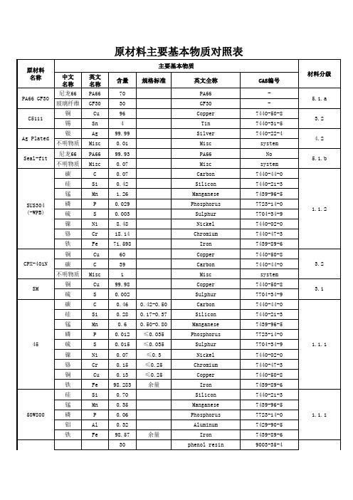
Iron Carbon Silicon Manganese Phosphorus Sulphur Nickel Chromium
Iron grease
Misc Carbon Silicon Manganese
CAS编号
7440-50-8 7440-31-5 7440-22-4 system No system 7440-44-0 7440-21-3 7439-96-5 7723-14-0 7704-34-9 7440-02-0 7440-47-3 7439-89-6 7440-50-8 7440-44-0 system 7440-50-8 7704-34-9 7440-44-0 7440-21-3 7439-96-5 7723-14-0 7704-34-9 7440-02-0 7440-47-3 7440-50-8 7439-89-6 7440-21-3 7439-96-5 7723-14-0 7429-90-5 7439-89-6 9003-35-4
原材料 名称
PA66 GF30 C5111
Ag Plated Seal-fit
SUS304 (-WPB)
CPX-401N SM
45
50W800
中文 名称 尼龙66 玻璃纤维
铜 锡 银 不明物质 尼龙66 不明物质 碳 硅 锰 磷 硫 镍 铬 铁 铜 碳 不明物质 铜 硫 碳 硅 锰 磷 硫 镍 铬 铜 铁 硅 锰 磷 铝 铁
-
100-97-0
557-05-1 10043-35-3
67-56-1 557-05-1
纳入GF 7440-50-8 7440-22-4 1317-36-8 7440-50-8
ASTM A751-2014a-中文版
目录序言 (1)1. 范围 (1)2. 引用文件 (2)3. 术语 (3)4. 关于化学成分要求的标准 (4)5. 铸造或熔炼分析 (4)6. 成品分析要求 (5)7. 非规定元素(注4) (5)8. 取样 (5)9. 试验方法 (6)10. 参考材料 (8)11. 有效位数 (8)12. 圆整方法 (8)13. 报告 (9)14. 关键词 (9)附录(非强制性资料) (10)变更一览表 (11)钢制品化学分析标准试验方法、实验操作和术语1本标准是以固定代号A751发布的。
其后的数字表示原文本正式通过的年号;在有修订的情况下,为上一次的修订年号;圆括号中数字为上一次重新确认的年号。
上标符号(ε)表示对上次修改或重新确定的版本有编辑上的修改。
本标准经批准被国防部机构采用。
序言本标准的制订的这些试验方法,实验规程和术语意在回答需要有一份获取和报告钢、不锈钢和相关合金的化学分析,包括其各个方面的惟一文件。
如术语的定义和成品(校核)分析偏差(公差)一类题目要求的解释。
而对于取样、符合规定的限值和数据处理上的要求,在已制订的产品标准中通常并不很清楚。
本标准的制订的这些试验方法,实验规程和术语打算包含对于测定钢、不锈钢和相关合金的化学成分的所有要求,从而产品标准将只需要包括特殊的修正和例外。
1. 范围1.1这些试验方法、试验操作和术语包括钢、不锈钢和合金的化学分析的定义、参考办法、规程和指导方针,包括湿式化学分析和仪器分析技术。
1.2为掌握化学要求、产品分析、残余元素和参考标准并为化学分析数据处理和报告提供指引。
1.3这些试验方法、试验操作和术语作为一项要求,只应用于包括这些试验方法,试验操作和术语或零部件在内的产品规范。
1.4当发生矛盾时,产品规范要求应优先于这些试验方法、试验操作和术语的要求。
1.5当对于实验室评估标准方面的信息有所要求时,可参见条例ISO/IEC 17025。
1.6本标准并没有完全列举所有的安全声明,如果有必要,根据实际使用情况进行斟酌。
ZTX751中文资料

-0.1 -10 -0.1 -0.15 -0.3 -0.28 -0.5 -0.9
Emitter Cut-Off Current
IEBO
-0.1 -0.15 -0.3 -0.28 -0.5 -0.9 -1.25
Collector-Emitter VCE(sat) Saturation Voltage Base-Emitter VBE(sat) Saturation Voltage
E-Line TO92 Compatible ZTX751 -80 -60 UNIT V V V A A W mW/°C °C
-55 to +200
ELECTRICAL CHARACTERISTICS (at Tamb = 25°C unless otherwise stated).
PARAMETER Collector-Base Breakdown Voltage Collector-Emitter Breakdown Voltage Emitter-Base Breakdown Voltage Collector Cut-Off Current SYMBOL V(BR)CBO V(BR)CEO V(BR)EBO ICBO UNIT CONDITIONS. V V V
PNP SILICON PLANAR MEDIUM POWER TRANSISTORS
ISSUE 2 JULY 94 FEATURES * 60 Volt VCEO * 2 Amp continuous current * Low saturation voltage * Ptot= 1 Watt
Transition Frequency Switching Times
fT ton toff
ASTM D751-2006 涂层织物标准测试法(中文版)

ASTM D751-2006涂层织物标准测试法(中文版)1.范围1.1 本测试法适用于防水、雨用的橡胶涂层织物和类似产品的测试。
1.2范围内的各种测试方法如下所示:1.3以下为测试方法:测试方法部分尺寸与质量7-10断裂强力11抓样法(方法A)12-15条样法(方法B)16伸长17顶破强力18-21抗穿刺性22-25撕破强力26落锤法(方法A)27舌形试样撕破强力法(方法B)28-31梯形撕破32-35耐水压36马伦式法(方法A)37-40水柱法(方法B)41-44粘合涂层45-48涂层强度49-53抗粘性涂层撕破法54-58低温弯曲测试59低温冲击测试60低温防爆裂能力61-65缝合强力66-71加速热老化(烘箱法)72-79定负荷接缝强力80-83高温抗粘滞性能84-88耐压89-93涂层布厚度94-981.1标准中值使用SI单位制,括号内的值仅做参考。
2.引用标准2.1ASTM标准D573 橡胶测试法——空气灶中的老化D1349 橡胶惯例——标准温度测试D1424 落锤式织物撕破强力测试仪的织物撕破强力测试法D2136 涂层橡胶的测试方法——低温弯曲法D2137 橡胶特性的测试方法——可挠性聚合物和涂层织物的脆变点D4483 在橡胶与炭黑工业标准测试法中的精确度的操作3.意义与用途3.1涂层织物和使用涂层织物生产的橡胶制品是商业中的一个重要部分,我们应该使用适当的方法来确定这些商品的质量,这些测试方法必须具有测试产品的能力。
4.标准大气4.1预调——涂层织物的测试环境如果没有记载,则应该满足4.2或4.3所规定的条件,或者是按照买方与供应商之间达成的协议。
当涂层织物在热的环境中测试时,对环境的要求如4.3记载。
4.2环境温度——测试涂层织物的标准条件应满足织物吸湿平衡的标准大气,其环境相对湿度为50±5%,温度为23±2℃。
4.3热环境——测试涂层织物的标准条件应满足织物吸湿平衡的标准大气,其环境相对湿度为65±5%,温度为27±2℃。
RB751SL;中文规格书,Datasheet资料
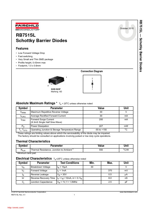
Absolute Maximum Ratings * T A = 25°C unless otherwise noted* These ratings are limiting values above which the serviceability of the diode may be impaired. The factory should be consulted on applications involving pulsed or low duty cycle operations.Thermal Characteristics* Minimum land pad.Electrical Characteristics T A =25°C unless otherwise notedSymbolParameterValueUnitV RRM Maximum Repetitive Reverse Voltage 30V I F(AV)Average Rectified Forward Current 30mA I FSM Forward Surge Current(8.3mS Single Half Sine-Wave)200mA P D Power Dissipation227mW T J, T STGOperating Junction & Storage Temperature Range-55 to +150°CSymbolParameterValueUnitR θJA Thermal Resistance, Junction to Ambient *550°C/WSymbolParameterTest ConditionsMin.Max.UnitV R Breakdown Voltage I R = 10μA 30V V F Forward Voltage I F = 1mA 370mV I R Reverse Leakage V R = 30V0.5μA trr Reverse Recovery Time I F = I R = 10mA, irr = 0.1I R8.0nS C jJunction CapacitanceV R = 1V, f = 1.0MHz2.5pFConnection Diagram2121SOD-923F Marking: ADThe following includes registered and unregistered trademarks and service marks, owned by Fairchild Semiconductor and/or its global subsidiaries, and is notAccuPower¥Auto-SPM¥Build it Now¥CorePLUS¥CorePOWER¥CROSSVOLT¥CTL¥Current Transfer Logic¥DEUXPEED®Dual Cool™ EcoSPARK®EfficientMax¥ESBC¥®Fairchild®Fairchild Semiconductor®FACT Quiet Series¥FACT®FAST®FastvCore¥FETBench¥FlashWriter®*FPS¥F-PFS¥FRFET®Global Power Resource SMGreen FPS¥Green FPS¥ e-Series¥G max¥GTO¥IntelliMAX¥ISOPLANAR¥MegaBuck¥MICROCOUPLER¥MicroFET¥MicroPak¥MicroPak2¥MillerDrive¥MotionMax¥Motion-SPM¥OptoHiT™OPTOLOGIC®OPTOPLANAR®®PDP SPM™Power-SPM¥PowerTrench®PowerXS™Programmable Active Droop¥QFET®QS¥Quiet Series¥RapidConfigure¥¥Saving our world, 1mW/W/kW at a time™SignalWise¥SmartMax¥SMART START¥SPM®STEALTH¥SuperFET®SuperSOT¥-3SuperSOT¥-6SuperSOT¥-8SupreMOS®SyncFET¥Sync-Lock™®*The Power Franchise®TinyBoost¥TinyBuck¥TinyCalc¥TinyLogic®TINYOPTO¥TinyPower¥TinyPWM¥TinyWire¥TriFault Detect¥TRUECURRENT¥*P SerDes¥UHC®Ultra FRFET¥UniFET¥VCX¥VisualMax¥XS™* Trademarks of System General Corporation, used under license by Fairchild Semiconductor.DISCLAIMERFAIRCHILD SEMICONDUCTOR RESERVES THE RIGHT TO MAKE CHANGES WITHOUT FURTHER NOTICE TO ANY PRODUCTS HEREIN TO IMPROVE RELIABILITY, FUNCTION, OR DESIGN. FAIRCHILD DOES NOT ASSUME ANY LIABILITY ARISING OUT OF THE APPLICATION OR USE OF ANY PRODUCT OR CIRCUIT DESCRIBED HEREIN; NEITHER DOES IT CONVEY ANY LICENSE UNDER ITS PATENT RIGHTS, NOR THE RIGHTS OF OTHERS. THESE SPECIFICATIONS DO NOT EXPAND THE TERMS OF FAIRCHILD’S WORLDWIDE TERMS AND CONDITIONS, SPECIFICALLY THE WARRANTY THEREIN, WHICH COVERS THESE PRODUCTS.LIFE SUPPORT POLICYFAIRCHILD’S PRODUCTS ARE NOT AUTHORIZED FOR USE AS CRITICAL COMPONENTS IN LIFE SUPPORT DEVICES OR SYSTEMS WITHOUT THE EXPRESS WRITTEN APPROVAL OF FAIRCHILD SEMICONDUCTOR CORPORATION.As used herein:1. Life support devices or systems are devices or systems which, (a) areintended for surgical implant into the body or (b) support or sustain life, and (c) whose failure to perform when properly used in accordance with instructions for use provided in the labeling, can be reasonably expected to result in a significant injury of the user. 2. A critical component in any component of a life support, device, orsystem whose failure to perform can be reasonably expected to cause the failure of the life support device or system, or to affect its safety or effectiveness.ANTI-COUNTERFEITING POLICYFairchild Semiconductor Corporation's Anti-Counterfeiting Policy. Fairchild's Anti-Counterfeiting Policy is also stated on our external website, , under Sales Support.Counterfeiting of semiconductor parts is a growing problem in the industry. All manufacturers of semiconductor products are experiencing counterfeiting of their parts. Customers who inadvertently purchase counterfeit parts experience many problems such as loss of brand reputation, substandard performance, failed applications, and increased cost of production and manufacturing delays. Fairchild is taking strong measures to protect ourselves and our customers from the proliferation of counterfeit parts. Fairchild strongly encourages customers to purchase Fairchild parts either directly from Fairchild or from Authorized Fairchild Distributors who are listed by country on our web page cited above. Products customers buy either from Fairchild directly or from Authorized Fairchild Distributors are genuine parts, have full traceability, meet Fairchild's quality standards for handling and storage and provide access to Fairchild's full range of up-to-date technical and product information. Fairchild and our Authorized Distributors will stand behind all warranties and will appropriately address any warranty issues that may arise. Fairchild will not provide any warranty coverage or other assistance for parts bought from Unauthorized Sources. Fairchild is committed to combat this global problem and encourage our customers to do their part in stopping this practice by buying direct or from authorized distributors.PRODUCT STATUS DEFINITIONSDefinition of TermsDatasheet Identification Product Status Definition分销商库存信息: FAIRCHILDRB751SL。
德威特751说明书
北京德威特恒通电力自动化设备有限公司硬件系列DVP - 751微机电源备自投保护监控装臵使用说明书北京德威特恒通电力自动化设备有限公司DVP-751微机电源备自投保护监控装置说明书目录1.本保护装置的适用范围 (1)2.装置技术数据 (1)3.结构说明 (4)3.1安装与开孔 (4)3.2装置组成 (5)4.装置配备的保护功能 (6)5.保护装置的原理图与装置端子接线说明 (10)5.1保护装置的原理图 (10)5.2装置端子图及接线说明 (11)6. 数码管的七种显示及按键的使用说明 (12)6.1数码管的七种显示 (12)6.2按键使用说明: (12)6.2.1输入密码的方法: (13)6.2.2输入修改保护定值的方法: (13)6.2.3打开与关闭保护控制字的方法: (13)6.2.4搜索的三种方法(适用于定点显示和进入定值区的显示): (14)6.3几种显示列表: (14)6.3.1正常循环显示(供运行人员使用) (14)6.3.2定点显示 (14)6.3.3进入定值区显示(输入密码1111) (16)6.3.4跳闸及报警信号指示 (17)7.调试大纲(适用于现场调试人员及检修维护人员) (18)7.1查看、输入或修改保护定值: (18)7.2开关量的检查 (18)7.3监控操作 (18)7.4保护继电器的出口检查 (19)7.5模拟量精度校准 (19)7.6保护试验 (20)7.6.1过流保护试验(低压闭锁) (20)北京德威特恒通电力自动化设备有限公司 1DVP-751微机电源备自投保护装置说明书北京德威特恒通电力自动化设备有限公司 2 7.6.2速断试验 (20)7.6.3备用电源自投测试 (20)7.6.4联锁跳闸 (21)7.6.5 过流后加速跳闸 (21)7.6.6 合环保护试验 (21)7.6.7 PT 断线报警 (21)7.6.8时间测试 (21)7.6.9控制回路断线预告 (21)7.6.10 CAN 网的连接 (21)7.7更换插件注意事项 (22)8.运行人员注意事项及要求 (22)9.检修及维护: (22)10.注意事项 (22)11.订货信息 ...................................................................... 错误!未定义书签。
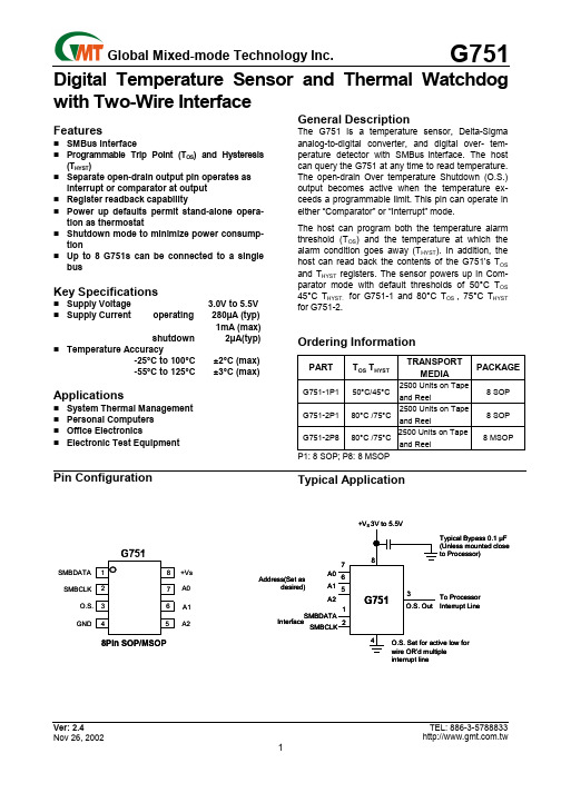
G751中文资料
with Two-Wire Interface FeaturesSMBus interfaceProgrammable Trip Point (T OS) and Hysteresis (T HYST)Separate open-drain output pin operates as interrupt or comparator at outputRegister readback capabilityPower up defaults permit stand-alone opera-tion as thermostatShutdown mode to minimize power consump-tionUp to 8 G751s can be connected to a single busKey SpecificationsSupply Voltage 3.0V to 5.5V Supply Current operating 280µA (typ)1mA (max)shutdown 2µA(typ) Temperature Accuracy-25°C to 100°C ±2°C (max)-55°C to 125°C ±3°C (max) ApplicationsSystem Thermal ManagementPersonal ComputersOffice ElectronicsElectronic Test Equipment General DescriptionThe G751 is a temperature sensor, Delta-Sigma analog-to-digital converter, and digital over- tem-perature detector with SMBus interface. The host can query the G751 at any time to read temperature. The open-drain Over temperature Shutdown (O.S.) output becomes active when the temperature ex-ceeds a programmable limit. This pin can operate in either “Comparator” or “Interrupt” mode.The host can program both the temperature alarm threshold (T OS) and the temperature at which the alarm condition goes away (T HYST). In addition, the host can read back the contents of the G751’s T OS and T HYST registers. The sensor powers up in Com-parator mode with default thresholds of 50°C T OS 45°C T HYST. for G751-1 and 80°C T OS , 75°C T HYST for G751-2.Ordering InformationPART T OS T HYSTTRANSPORTMEDIAPACKAGE G751-1P1 50°C/45°C2500 Units on Tapeand Reel8 SOPG751-2P1 80°C/75°C2500 Units on Tapeand Reel8 SOPG751-2P8 80°C/75°C2500 Units on Tapeand Reel8 MSOP P1: 8 SOP; P8: 8 MSOPTypical ApplicationSMBDATA8Pin SOP/MSOP +Vs A0 A1 A2SMBCLKGND Address(Set asInterfaceinterrupt line desired)A0A1A2Supply Voltage………….…………………-0.3V to 6.5V Voltage at any Pin……………….…-0.3V to +Vs +0.3V Input Current at any Pin…………………………….5mA Package Input Current…………………………….20mA O.S. Output Sink Current………………………….10mA O.S. Output Voltage…………………….…………..6.5V Storage Temperature…………………-65°C to +150°C Soldering Information, Lead TemperatureSOP PackageVapor Phase (60 seconds)……………………….215°C Infrared (15 seconds)……………………………..220°C ESD SusceptibilityHuman Body Model (2000V)Machine Model……………………………………...200V Specified Temperature Range…………….T MIN to T MAX-55°Cto+125°C Supply Voltage Range (+Vs)…………..+3.0V to +5.5VTemperature-to-Digital Converter CharacteristicsUnless otherwise noted, these specifications apply for +Vs=+3.3v Vdc. Boldface limits apply for T A=T J=T MIN toT MAX; all other limits T A=T J= +25°C, unless otherwise noted.PARAMETER CONDITIONSTYPICALLIMITSUNITSAccuracy TA=-25°C to +100°CTA=-55°C to +125°C±2.0±3.0 °C (max)Resolution9BitsTemperature Conversion Time 100 MsQuiescent Current SMBus InactiveSMBus ActiveShutdown Mode0.2511.0MamA (max)µAO.S. Output Saturation Voltage I OUT = 4.0mA 0.8 V (max)O.S. Delay 16Conversions (min)Conversions (max)T OS Default Temperature G751-1/G751-2 50/80 °C T HYST Default Temperature G751-1/G751-2 45/75 °CBlock DiagramA0SMBDATAA1A2SMBCLKDigital DC CharacteristicsUnless otherwise noted, these specifications apply for +Vs=+3.3 Vdc. Boldface limits apply for T A =T J =T MIN to T MAX ; all other limits T A =T J =+25°C, unless otherwise noted. SYMBOL PARAMETER CONDITIONS TYPICAL LIMITS UNITSV IN (1) Logical “1” Input Voltage +Vs × 0.7 +Vs + 0.5 V (min) V (max) V IN (0) Logical “0” Input Voltage-0.3 +Vs ×0.3V (min) V (max) I IN (1) Logical “1”Intput Current V IN =5V 0.005 1.0 µA I IN (0) Logical “0”Intput Current V IN =0V -0.005 -1.0µA C IN All Digital Inputs20 PF I OH High Level Output Current V OH =5V 100 µA (max) V OL Low Level Output Voltage I OL =3ma 0.4 V (max) t OFOutput Fall TimeC L =400pF,I O =3ma 250ns (max)SMBus Digital Switching CharacteristicsUnless otherwise noted, these specifications apply for +Vs = +3.3 Vdc and C L (load capacitance) on output lines = 80pF unless otherwise specified. Boldface limits apply for T A = T J = T MIN to T MAX ; all other limits T A = T J = +25°C, unless otherwise noted.The switching characteristics of the G751 fully meet or exceed the published specifications of the SMBus. The following parameters are the timing relationships between SMBCLK and SMBDATA signals related to the G751. They are not the SMBus specifications.SYMBOL PARAMETER CONDITIONS TYPICAL LIMITSUNITSt 1 SMBCLK (Clock) Period2.5 µs (min) t 2 Data in Set-Up Time to SMBCLK High 100 ns (min) t 3 Data Out Stable after SMBCLK Low0 ns (min) t 4 SMBDATA Low Set-Up Time to SMBCLK Low (Start Condition) 100 ns (min) t 5SMBDATA High Hold Time after SMBCLK High (Stop Condition)100ns (min)Pin DescriptionPIN LABELFUNCTIONTYPICAL CONNECTION1 SMBDATA SMBus Serial Bi-Directional Data Line From Controller2 SMBCLK SMBus Clock Input From Controller3 O.S. Overtemperature Shutdown Open Drain Output Pull Up Resistor, Controller Interrupt Line4 GND Power Supply GroundGround5,6,7 A0-A2 User-Set SMBus Address Inputs Ground (Low, “0”) or +Vs (High, “1”) 8 +Vs Positive Supply Voltage InputDC Voltage from 3V to 5.5VLogic Electrical CharacteristicsSMBDATASMBDATA SMBCLKData inData outTemperature-to-Digital Transfer Function (Non-linear scale for clarity)Functional DescriptionThe G751 temperature sensor incorporates a band-gap type temperature sensor and 9-bit ADC (Delta-Sigma Analog- to-Digital Converter). The temperature data output of the G751 is available at all times via the SMBus. If a conversion is in pro-gress, it will be stopped and restarted after the read.A digital comparator is also incorporated that com-pares a series of readings, the number of which is user-selectable, to user-programmable setpoint and hysteresis values. The comparator trips the O.S. output line, which is programmable for mode and polarity.O.S. Output, T OS and T HYST LimitsIn Comparator mode the O.S. Output behaves like a thermostat. The output becomes active when tem-perature exceeds the T OS limit, and leaves the active state when the temperature drops below the T HYST limit. In this mode the O.S. output can be used to turn a cooling fan on, initiate an emergency system shutdown, or reduce system clock speed. Shutdown mode does not reset O.S. state in a comparator mode.In interrupt mode exceeding T OS also makes O.S. active but O.S. will remain active indefinitely until reset by reading any register via the SMBus inter-face. Once O.S. has been activated by crossing T OS, then reset, it can activated again only by Tempera-ture going below T HYST. Again, it will remain active indefinitely until being reset by a read. Placing the G751 in shutdown mode also resets the O.S. output. Default ModesG751 always powers up in a known state. G751 power up default conditions are:1. Comparator mode2. T OS set to 50°C for G751-1, to 80°C for G751-23. T HYST set to 45°C for G751-1, to 75°C for G751-24. O.S. active low5. Pointer set to “00”; Temperature RegisterWith these operating conditions G751 can act as a stand-alone thermostat with the above temperature settings. Connection to an SMBus is not required. SMBus InterfaceThe G751 operates as a slave on the SMBus, so the SMBCLK line is an input (no clock is generated bythe G751) and the SMBDATA line is a bi-directional serial data path. According to SMBus specifications,the G751 has a 7-bit slave address. The four most significant bits of the slave address are hard wired inside the G751 and are “1001”. The three least sig-nificant bits of the address are assigned to pinsA2-A0, and are set by connecting these pins to ground for a low, (0); or to +Vs for a high, (1). Therefore, the complete slave address is:1 0 0 1 A2 A1 A0 MSB LSBFigure1 O.S. Output Temperature Response Diagram Temperature Data FormatTemperature data can be read from the Temperature, T OS Set Point, and T HYST Set Point registers; and written to the T OS Set Point, and T HYST Set Point reg-isters. Temperature data is representedby a 9-bit, two’s complement word with an LSB (Least Significant Bit) equal to 0.5°C:DIGITAL OUTPUTTEMPERATUREBINARY HEX+125°C 0 1111 1010 0FAh +25°C 0 0011 0010 032h +0.5°C 0 0000 0001 001h 0°C 0 0000 0000 000h -0.5°C 1 1111 1111 1FFh -25°C 1 1100 1110 1CEh -55°C 1 1001 0010 192hShutdown ModeShutdown mode is enabled by setting the shutdown bit in the Configuration register via the SMBus. Shut-down mode reduces power supply current to 1 µA typical. In interrupt mode O.S. is reset if previously set and is undefined in Compatator mode during shutdown. The SMBus interface remains active. Ac-tivity on the clock and data lines of the SMBus may slightly increase shutdown mode quiescent current. T OS , T HYST , and Configuration registers can be read from and written to in shutdown mode.Fault QueueA fault queue of up to 6 faults is provided to prevent false tripping of O.S. when the G751 is used in noisy environments. The number of faults set in the queue must occur consecutively to set the O.S. output. Comparator/Interrupt ModeAs indicated in the O.S. Output Temperature Re-sponse Diagram, Figure 1, the events that trigger O.S. are identical for either Comparator or Interrupt mode. The most important difference is that in Inter-rupt mode the O.S. will remain set indefinitely once it has been set. To reset O.S. while in Interrupt mode, perform a read from any register in the G751. O.S. OutputThe O.S. output is an open-drain output and does not have an internal pull-up. A ”high” level will not be observed on this pin until pull-up current is provided from some external source, typically a pull-up resis-tor. Choice of resistor value depends on many sys-tem factors but, in general, the pull-up resistor should be as large as possible. This will minimize any errors due to internal heating of the G751. The maximum resistance of the pull up, based on G751 specification for High Level Output Current, to pro-vide a 2V high level, is 30k Ω.O.S. PolarityThe O.S. output can be programmed via the con-figuration register to be either active low (default mode), or active high. In active low mode the O.S. output goes low when triggered exactly as shown on the O.S. Output Temperature Response Diagram, Figure 1. Active high simply inverts the polarity of the O.S. output.T T O ST H Y S TO .S .(C o m p a r a t o r M o d e )O .S .(I n t e r r u p t M o d e )e m p e r a t u S h o w nf o r O .S . s e t f o r a c t i v e l o w .*r e a d a n y r e g i s t e r o r p l a c e d i n s h u t d o w nThere are four data registers in the G751, selected by the Pointer register. At power-up the Pointer is set to “00”; the location for the Temperature Register. The Pointer register latches whatever the last loca-tion it was set to. In Interrupt Mode, a read from the G751, or placing the device in shutdown mode, re-sets the O.S. output. All registers are read and write, except the Temperature register which is read only. A write to the G751 will always include the address byte and the Pointer byte. A write to the Configura-tion register requires one data byte, and the T OS and T HYST registers require two data bytes.Reading the G751 can take place either of two ways: If the location latched in the Pointer is correct (most of the time it is expected that the Pointer will point to Temperature register because it will be the data most frequently read from the G751), then the read can simply consist of an address byte, followed by retrieving the corresponding number of data bytes. If the Pointer needs to be set, than an address byte, pointer byte, repeat start, and another address byte will accomplish a read.The first data byte is the most significant byte with most signification bit first, permitting only as much data as necessary to be read to determine tempera-ture condition. For instance, if the first four bits of the temperature data indicates an overtemperature con-dition, the host processor could immediately take action to remedy the excessive temperatures. At the end of a read, the G751 can accept either Acknowl-edge or No Acknowledge from the Master (No Ac-knowledge is typically used as a signal for the salve that the Master has read its last byte).An inadvertent 8-bit read from a 16-bit register, with the D7 bit low, can cause the G751 to stop in a state where the SDA line is held low as shown in Figure 2. This can prevent any further bus communication until at least 9 additional clock cycles have occurred. Al-ternatively, the master can issue clock cycles until SDA goes high, at which time issuing a “Stop” condi-tion will reset the G751.Figure 2. Inadvertent 8-Bit Read from 16-Bit Register where D7 is ZeroMaster but G751 locks SMBDATA low Master detects the errorSMBCLKSMBDATAIntended Stop byof its ways(Selects which registers will be read from or written to):P7 P6 P5 P4 P3 P2 P1 P00 0 0 0 0 0 RegisterSelectP0-P1 :Register Select:P1 P0 REGISTER0 0 Temperature (Read only) (Power-up default)Configuration(Read/Write)0 1T HYST (Read/Write)1 0T OS (Read/Write)1 1P2-P7 :Must be kept zero.Temperature Register(Read Only):D15 D14 D13 D12 D11 D10 D9 D8 D7 D6 D5 D4 D3 D2 D1 D0MSB Bit 7 Bit 6 Bit 5 Bit 4 Bit 3 Bit 2 Bit 1 LSB X X X X X X XD0-D6 :UndefinedD7-D15 :Temperature Data. One LSB = 0.5°C. Two’s complement format.Configuration Register(Read/Write):D7 D6 D5 D4 D3 D2 D1 D0Cmp/IntShutdownPolarity0 0 0 FaultO.S.QueuePower up default is with all bits “0” (zero).D0 :Shutdown : When set to 1 the G751 goes to low power shutdown mode.D1 :Comparator / Interrupt mode : 0 is Comparator mode, 1 is Interrupt mode.D2 :O.S. Polarity : 0 is active low, 1 is active high. O.S. is an open-drain output under all conditions.D3-D4 :Fault Queue : Number of faults necessary to detect before setting O.S. output to avoid false tripping dueto noise :OFFAULTS D4 D3NUMBER0 0 1 (Power-up default)0 1 21 0 41 1 6D5-D7 :These bits are used for production testing and must be kept zero for normal operation.T HYST and T OS Register(Read/Write):D15 D14 D13 D12 D11 D10 D9 D8 D7 D6 D5 D4 D3 D2 D1 D0MSB Bit 7 Bit 6 Bit 5 Bit 4 Bit 3 Bit 2 Bit 1 LSB X X X X X X XD0-D6 :UndefinedD7-D15 :T HYST Or T OS Trip Temperature Data. Power up default is T OS = 50°C /80°C for G751-1/G751-2, T HYST =45°C /75°C for G751-1/G751-2.StartG751AckStartG751Master NoCondRepeat Ack Ack No Cond StartG751G751CondbyMasterAddress Byte AckbyPointer BytebyG751byMasterAddress Byte AckbyMost Significant Data ByteAckbyAckbyMasterStopbyMasterLeast Significant Data ByteStartby Master Address BytebyG751Most Significant Data BytebyMasterAckbyMasterStopbyMasterLeast Significant Data BytebyMasterAddress Byte AckbyPointer ByteAckbyStopbyMasterS n S A A A S A A A C t o p C o d b y M a s t e rt a r t b y M a s t e rA d d r e s sB y t ec k b y G 751P o i n t e r B y t e c k b y M a s t e r N o A c k b y M a s t e r A d r e s s B y t e919199R e p e a t S t a r t b y M a s t e r D a t a B y t ec k b y G 751t a r t b y M a s t e rA d d r e s sB y t ec k b y G 751P o i n t e r B y t e c k b y M a s t e r c k b y G 751S t o p o n d b y M a s t e rC o n f i g u r a t i o n B y t et o p o n d b y s t e r1(a ) T y p i c a l P o i n t e r S e t f o l l o w e d b y I m m e d i a t e R e a d f r o m C o n f i g u r a t i o n R e g i s t e r(b ) C o n f i g u r a t i o n R e g i s t e r W r i t e(c ) T O S a n d T H Y S T W r i t e8 Pin SOP PackageNote:1. Package body sizes exclude mold flash and gate burrs2. Dimension L is measured in gage plane3. Tolerance 0.10mm unless otherwise specified4. Controlling dimension is millimeter converted inch dimensions are not necessarily exact.DIMENSION IN MM DIMENSION IN INCHSYMBOLMIN. NOM. MAX. MIN. NOM. MAX.A 1.35 1.60 1.75 0.053 0.063 0.069 A1 0.10 ----- 0.25 0.004 ----- 0.010 A2 ----- 1.45 ----- ----- 0.057 -----B 0.33 ----- 0.51 0.013 ----- 0.020C 0.19 ----- 0.25 0.007 ----- 0.010D 4.80 ----- 5.00 0.189----- 0.197 E 3.80 ----- 4.00 0.150 ----- 0.157 e ----- 1.27 ----- ----- 0.050 ----- H 5.80 ----- 6.20 0.228 ----- 0.244 L 0.40 ----- 1.27 0.016 ----- 0.050 y ----- ----- 0.10 ----- ----- 0.004 θ 0º ----- 8º 0º ----- 8ºVer: 2.4Nov 26, 2002TEL: 886-3-5788833 118 Pin MSOP PackageDIMENSION IN MM DIMENSION IN INCHSYMBOLMIN. NOM. MAX. MIN. NOM. MAX.A ----- ----- 1.10 ----- ----- 0.043 A1 0.05 ----- 0.15 0.002 ----- 0.006A2 0.81 0.86 0.91 0.032 0.034 0.036 b 0.25 ----- 0.40 0.008----- 0.012b1 0.25 0.30 0.35 0.010 0.012 0.014 c 0.13 ----- 0.23 0.005 0.009 c1 0.13 0.15 0.18 0.005 0.006 0.007 D 2.90 3.00 3.10 0.114 0.118 0.122 E1 2.90 3.00 3.10 0.1140.118 0.122 e 0.65 BSC 0.026 BSC E 4.90 BSC 0.193 BSC L 0.445 0.55 0.648 0.0175 0.0217 0.0255 θ1 0° ----- 6° 0° ----- 6° θ2 12 REF 12 REF θ3 12 REF 12 REF R 0.09 ----- ----- 0.004 ----- ----- R1 0.09 ----- ----- 0.004 ----- ----- JEDEC MO-187AATaping SpecificationGMT Inc. does not assume any responsibility for use of any circuitry described, no circuit patent licenses are implied and GMT Inc. reserves the right at any time without notice to change said circuitry and specifications.Typical SOP/MSOP Package OrientationC b1E18E1DETAIL “A”Leb DA2AA1SEATING PLANEbWITH PLATINGBASE METALc1cθ1GAUGE PLANE0.25RR1Lθ3θ2元器件交易网。