Class D Audio Amplifier Basics
class d 原理(一)

class d 原理(一)Class D 概述什么是 Class DClass D 是一种用于放大音频信号的功率放大器。
它具有高效、节省能源和低发热等优点,因此在音频应用场景中得到广泛应用。
Class D 的原理1.脉宽调制(PWM)技术:Class D 使用脉宽调制技术将模拟音频信号转换为数字信号。
这通过将音频信号分成许多短时脉冲来实现,其宽度与音频信号的幅度有关。
2.输出滤波:脉宽调制后的数字信号需要经过输出滤波电路来去除高频成分。
输出滤波器使用电感和电容来滤除脉宽调制信号中的高频元素,以得到音频信号的纯净输出。
3.开关管:Class D 使用开关管(通常是 MOSFET)将滤波后的数字信号转换回模拟信号。
开关管的导通和截止由输入信号的 PWM 脉冲控制,从而根据输入信号的幅度调整输出信号的幅度。
Class D 的优点•高功率效率:Class D 的功率效率通常非常高,因为开关管只在导通和截止状态工作,并且能量损失小。
•节能环保:由于高功率效率,Class D 在相同输出功率的情况下消耗的电能较少,有助于节能和减少能源浪费。
•低发热:相比于传统的线性放大器,Class D 发热较少,这是因为开关管处于导通和截止状态而不会持续工作。
•小体积:Class D 的电路结构相对简单,所需元器件较少,因此可以实现较小的物理体积。
Class D 的应用•低音扬声器:Class D 可以提供高功率输出,使其成为低音扬声器的理想放大器。
•汽车音响:由于 Class D 的高效特性,许多汽车音响系统采用 Class D 放大器,以提供强大的声音输出同时保持能耗低。
•蓝牙扬声器:蓝牙扬声器通常需要小体积和长电池寿命,Class D 放大器满足了这些要求。
•无线麦克风系统:Class D 可以提供清晰、高保真的音频输出,因此用于无线麦克风系统可以获得优异的音质表现。
总结Class D 是一种高效、节能、小体积的功率放大器,使用脉宽调制技术将模拟音频信号转换为数字信号,并通过开关管和输出滤波实现音频信号的放大和滤波。
Audio Basics 1
音频基础之声音的特性Presented By: Kane ZhangAudio Basics 1 ‒ Properties of Sound亚太区技术支持Citrix“Go To Training”Kane Zhang Email Address: kzhang@Cell in Hongkong: +852-********Cell in China: +86-156********Skype: biamp.kanezhangBiamp Systems | 9300 SW Gemini Dr. Beaverton, OR 97008 | tel: 800.826.1457 503.641.7287 | fax: 503.626.0281声音是什么?声音的特性什么是dB ?等响曲线 平方反比定律 今天给大家介绍… …,音频系统 室内声学特性 声学增益 声音信号级别 平衡与非平衡连接声音的定义:物理学:▪声波,是由振动物体产生,并在媒介中传播。
声波可以理解为介质偏离平衡态的小扰动的传播。
这个传播过程只是能量的传递过程,而不发生质量的传递。
生物学:▪是指声波作用于听觉器官所引起的一种主观感觉。
小问题:声音在真空里可以传播吗?声波声音的特性:声音物理特性:频率强度声谱(频谱)人耳主观感觉:音调响度音色小问题:音色和音调有什么不同?声音的特性: Harmonics 谐波/泛音 复合音基波一次泛音 二次泛音 三次泛音 四次泛音 中音C = 523 Hz 小常识:泛音是基波频率的整数倍声音的特性: ½ cycle 1 cycle WavelengthAmplitude P r e s s u r e 0+- 速度、周期、波长、频率、振幅、频宽声音的速度与媒介的温度和密度有关空气中的速度= 331.4 + 0.6 x T(ºC) m/s周期(T ):完成往復運動一次所需的時間。
单位:s 频率(F ):周期的倒数即f=1/T 单位:Hz波长(λ):指沿着波的传播方向,在波的图形中相对平衡位置的位移时刻相 同的相邻的两个质点之间的距离。
3瓦D类功放(TA8803)规格书
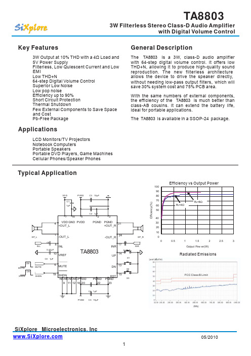
E f f i c i e n c y (%)Key FeaturesGeneral Description3W Output at 10% THD with a 4Ω Load and 5V Power SupplyFilterless, Low Quiescent Current and Low EMIThe TA8803 is a 3W, class-D audio amplifier with 64-step digital volume control. It offers low THD+N, allowing it to produce high-quality sound reproduction. The new filterless a r chitecture Low THD+Nallows the device to drive the speaker directly, 64-step Digital Volume Control Superior Low Noise Low pop noiseEfficiency up to 90% Short Circuit Protection Thermal ShutdownFew External Components to Save Space and Costwithout needing low-pass output filters , which will save 30% system cost and 75% PCB area.With the same numbers of external components, the efficiency of the TA8803 is much better than class-AB cousins. It can extend the battery life, ideal for portable applications.Pb-Free PackageApplicationsThe TA8803 is available in a SSOP-24 package.LCD Monitors/TV Projectors Notebook Computers Portable SpeakersPortable DVD Players, Game Machines Cellular Phones/Speaker PhonesTypical ApplicationVD DC11μFPVDDC3 10μFC2 1μF100 90 80 70 60 50 7 18 5 2 340 4VDD GND PVDD PGND PGND 21 30SP_L+OUT_L1-OUT_L +OUT_R24 -OUT_RSP_R20 10 0 0 0.5 1 1.5 2 2.5 3IN LC60 .47μF8 17 INL INR TA8803C70.47μFINROutput P ow er(W)10C8 1μFVREFUP 14S1 Radiated EmissionsONMUTEONMUTE6 MUTE DN13S2SHDNSHDN19 SHDNNC N C N CNCPVDDPGND RST15PGND S3FCC Class B Limit9 11 12 16 2022 23C4 1μFPVDDC5 10μFBlock DiagramVDD PGNDDNMUTE SHDN +OUT_R -OUT_RVREFINL+OUT_L-OUT_L PGNDPin Configuration & Marking InformationTop ViewSSOP-24-OUT_L 1 PGND 2 PGND 3 +OUT_L 4 PVDD 5 MUTE 6VDD 7INL 8NC 924 -OUT_R23 PGND22 PGND21 +OUT_R20 PVDD19 SHDN18 GND17 INR16 NCX: Internal CodeY: YearWW: WeekLL: Internal CodeVREF10NC 1115 RST 14 UPNC DNTA8803 XXXYWWLLPin DescriptionsAbsolute Maximum RatingsThese are stress ratings only and functional operation is not implied.Exposure to absolute maximum ratings for prolonged time periods may affect device reliability. All voltages are with respect to ground.Supply Voltage at no Input Signal...................6.0V Maximum Junction Temperature..................150°CInput Voltage.............................-0.3V to VDD +0.3V StorageTemperature.....................-65°C to 150°C Soldering Temperature.......................300°C, 5secRecommended Operating ConditionsSupply voltage Range........................2.2V to 5.5V Ambient Temperature Range...........-40°C to 85°CJunction Temperature Range.........-40°C to 125°CThermal InformationParameter Symbol Package Maximum Unit Thermal Resis tance (Junction to Ambient)θJA SSOP-2496°C/WElectrical CharacteristicVDD =5V, Gain = 18dB, RL=8Ω,TA=25°C,unless otherwise noted.Typical Operating Characteristics (TA=25°C)1. THD+N vs Output Power2. THD+N vs Output PowerR=8Ω, Gain = 18dB%0.% 0.50.0.0.00.00.010m20m50m100m200m500m12410m20m50m100m 200m500m 124W W3. THD+N vs Output PowerVDD =5V, RL=4Ω, Gain = 18dB4. THD+N vs Output PowerV=5V, R=8Ω, Gain = 18dB0 0 0W20m50m 100m 200m 500m 1 2 4W5. THD+N vs FrequencyVDD=5V, RL=4Ω, Gain = 18dB16. THD+N vs FrequencyV=5V, R=8Ω, Gain = 18dB00 00H z 0H zHzTypical Operating Characteristics (continued)7. THD+N vs. FrequencyPo=0.8W,R =4Ω,Gain=18dB18. THD+N vs. FrequencyPo=0.1W,R L =8Ω,Gain=18dB0020501002005001k2k5k10kH z20k0H z++9. Frequency responseV DD =5V, Gain =18dB10. Power Supply Ripple Rejection VS FrequencyV DD =5V with 200mVpp Ripple++d +--d-+-20 50 100 200 500 1k 2k 5k 10k Hz20k-H zd BV ------11. FFT of Noise OutputV =5V, Gain = 18dB-dB12.Channel SeparationV =5V, R =4Ω, P =1.0W,Gain = 18dB H zH zO u t p u t P o w e r (W )O u t p u t P o w e r (W )Typical Operating Characteristics (continued)43.53 2.521.510.50 13. Output Power vs Power SupplyR L =4Ω10%ΤΗD1%ΤΗD2 3 4 5 6Supply Voltage (V)2.52 1.51 0.50 14. Output Power vs Power SupplyR L =8Ω10%ΤΗD1%ΤΗD2 3 4 5 6Supply V o ltage (V )Gain Setting (VDD=5V)Step Gain (dB) Step Gain (dB)Step Gain (dB)Step Gain (dB)1 -75.0 17 4.83311.249 17.62 -39.7 18 5.13411.650 18.03 -34.0 19 5.53512.051 18.44 -28.2 20 5.93612.352 18.85 -22.4 21 6.33712.753 19.26 -16.5 22 6.73813.254 19.67 -10.5 23 7.13913.655 20.08 -8.0 24 7.54014.056 20.49 -5.5 25 7.94114.457 20.910 -2.9 26 8.34214.858 21.311 -0.4 27 8.74315.259 21.712 1.1 28 9.14415.660 22.113 2.6* 29 9.64516.061 22.514 3.6 30 10.04616.462 22.915 4.0 31 10.44716.863 23.4164.43210.74817.26423.8*Power on gain or gain after reset.Note: Gain could have 1dB deviation device to device.Application Notice1. When TA8803 works without filter, we must connect the speaker before turn on. Else, it will be easy to damage the chip.2. When TA8803 works without filter, it will be best that adding a ferrite chip bead at the outgoing line of speaker in order to suppress possible electromagnetic interference .3. The absolute maximum rating of operation voltage is 6.0V. While using 6V power regulator, even the chip can deliver 4W sine wave with a 4 Ohm speaker, it is not recommended for long term using due to the heat dissipation. But if the input signal is a music signal, then it can work in long term since the average power output is much less than 4W. When using dry battery cell,we should notice that if the battery cell is 4 new dry batteries or alkaline batteries, even the voltage will be over 6V, it still can work safety. Since the output voltage of the 4 pack of new dry batteries will be reduced very quickly after turn on due to the internal resistance of the battery. There is no dangerous of damaging the chip when playing music or speech, even use 4 new dry batteries. To reduce the effect of the increasing of internal resistance of battery after long term discharging, it is recommended to connect a 1000uF electrolytic capacitor between the power supply and the ground.4. Because digital volume control has big gain, we can not make input signal too high to cause the clipping of the output signal when increase volume, also it may damage the chip.Test Setup for Performance TestingTA8803 Demo Board1. The AP AUX-0025 low pass filter is necessary for every class-D amplifier measurementdone by AP analyzer.2. Two 22μH inductors are used in series with load resistor to emulate the small speaker forefficiency and quiescent current measurement.13Application InformationMaximum GainAs shown in block diagram(page 2),the TA8803 has two internal amplifiers stage. The first stage's gain is externally con figurable, while the second stage's is internally fixed in a fixed-gain, inverting configuration. The closed-loop gain of the first stage is set by selecting the ratio of R f to R i while the second stage's gain is fixed at 2x. Consequently, the differential gain for the IC isA VD =20*log [2*(R f /R i )]There are 64 discrete gain settings ranging from +24dB maximum to -75dB minimum. Upon device power on or applied a logic low to the RST pin, the amplifier's gain is set to a default value of -4.5dB. However, when coming out of mute mode, the TA8803 will revert back to its previous gain setting. Volume levels for each step vary and are specified in Gain Setting table on page 7.If both the UP and DN pins are held high, no volume change will occur. Trigger points for the UP and DN pins are at 70% of V DD minimum for a The TA8803 sets maximum R f =218k Ω and logic high, and 20% of V DD maximum for a logic minimum R i =27k Ω, thus the maximum closed- low. It is recommended, however, to toggle UP gain is 24dB.Digital Volume Control (DVC)The TA8803 features a digital volume control which consists of the UP, DN and RST pins. An a n d D N b e t w e e n V D D performance.a n d G N D f o rb e s t internal clock is used where the clock frequency value is determined from the following formula:f CLK = f OSC / 2The oscillator frequency f OSC Figure 1.Timming DiagramMute Operationvalue is 250kHz typical,with ±20% tolerance.The DVC’s clock The MUTE pin is an input for controlling the frequency is 33Hz (cycle time 30ms) typical.Volume changes are then effected by toggling either the UP or DN pins with a logic low. After a period of 3.5 clocks pulses with either the UP or DN pins held low, the volume will change to the next specified step, either UP or DN, and followed by a short delay. This delay decreases the longer the line is held low, eventually reaching a delay of zero. The delay allows the user to pull the UP or DN terminal low once for one volume change, or hold down to ramp several volume changes. The delay is optimally configured for push button volume control.If either the UP or DN pin remains low after the first volume transition the volume will change again, but this time after 9.5 clock pulses. The followed transition occurs at 2 clock pulses for each volume transition. This is intended to provide the user with a volume control that pauses briefly after initial application, and then slowly increases the rate of volume change as it is continuously applied. This cycle is shown in the timing diagram shown in figure 1.output state of the TA8803 . A logic low on this pin disables the outputs, and a logic high on this pin enables the outputs. This pin may be used as a quick disable or enable of the outputs without a volume fade. Quiescent current is listed in the electrical characteristic table. The MUTE pin can be left floating due to the pull-up internal.Shutdown operationIn order to reduce power consumption while not in use, the TA8803 contains shutdown circuitry that is used to turn off the amplifier's bias circuitry. T his shutdown feature t urns the amplifier off when logic low is placed on the SHDN pin. By switching the SHDN pin connected to GND, the TA8803 supply current draw will be minimized in idle mode. The SHDN pin cannot be left floating due to the pull-down internal.Power supply decouplingThe TA8803 is a high performance CMOS audio amplifier that requires adequate power supply decoupling to ensure the output THD and PSRR are as low as possible. Power supply decoupling is affecting low frequency response. Optimum decoupling is achieved by using two capacitors of different types that target different types of noise on the power supply leads. For higher frequency transients, spikes, or digitalhash on the line, a good low equivalent-series- resistance (ESR) ceramic capacitor, typically 1.0μF, placed as close as possible to the device function is to reduce noise produced by the power supply caused by coupling into the output drive signal. This noise is from the internal analog reference to the amplifier , which appears as degraded PSRR and THD+N.Bypass capacitor (C BYP ) values of 0.47μF to 1.0μF ceramic is recommended for the best THD and noise performance. Increasing the bypass capacitor reduces clicking and popping noise from power on/off and entering and leaving shutdown.Under Voltage Lock-out (UVLO)V DD terminal works best. For filtering lower- frequency noise signals, a larger capacitor of The TA8803 incorporates circuitry designed to 10μF (ceramic) or greater placed near the audio detect when the supply voltage is low. When the power amplifier is recommended.Input Capacitor (C i )Large input capacitors are both expensive and space hungry for portable designs. Clearly, a certain sized capacitor is needed to couple in low frequencies without severe attenu ation. But in many cases the speakers used in portable systems, whether internal or external, have little ability to reproduce signals below 100Hz to 150Hz. Thus, using a large input capacitor may not increase actual system perfor mance. In this case, input capacitor (C i ) and input resistance (R i ) of the amplifier form a high-pass filter with the corner frequency determined equation below, supply voltage drops to 1.85V or below, the TA8803 outputs are disable, and the device comes out of this state and starts to normal functional when the supply voltage increases.Short Circuit Protection (SCP)The TA8803 has short c ircuit protectioncircuitry on the outputs that prevents damage to the device during output-to-output and output- to-GND short. When a short circuit is detected on the outputs, the outputs are disable immediately. If the short was removed, the device activates again.Over Temperature Protectionf C =1 2πR i C iIn addition to system cost and size, click and pop perfor mance is affected by the size of the input coupling capacitor, C i . A larger input coupling capacitor requires more charge to reach itsThermal protection on the TA8803 prevents damage to the device when the internal die temperature exceeds 150°C. There is a 15 degree tolerance on this trip point from device to device. Once the die temperature exceeds the thermal s e t point, t h e device outputs a r e fault. The thermal quiescent DC voltage (nominally 1/2 V DD ). This charge comes from the internal circuit via the feedback and is apt to create pops upon device enable. Thus, by minimizing the capacitor size based on necessary low frequency response, turn-on pops can be minimized.Analog Reference Bypass Capacitor (C BYP )The Analog Reference Bypass Capacitor (C BYP ) is the most critical capacitor and serves several important functions. During start-up or recovery from shutdown mode, C BYP determines the rate at which t h e amplifier s t arts up. The s e conddisabled. This is not a latched fault is cleared once the temperature of the die is reduced by 60°C. This large hysteresis will prevent motor boating sound well and the device begins normal operation at this point with no external system interaction.How t o Reduce EMI (Electro Magnetic Interference)A simple solution is to put an additional capacitor 1000uF at power supply terminal for power line coupling if the traces from a mplifier to speakers are short (<20cm).05/201011Most applications require a ferrite bead filter which shows at Figure 3. The ferrite filter reduces EMI around 1 MHz and higher. When selecting a ferrite bead, choose one with high i m p e da nc e a t h i g h f r e q u en c ie s , b u t low impedance at low frequencies.channel specific. A two channels amplifier has t w o m u t u a l l y e x c l u s i v e c h a n n e l s a n d consequently must have two mutually exclusive output noise ground traces. The layout of the TA8803 offers separate PGND connections for each channel and in some cases each side of the bridge. Output noise grounds must tie to system ground at the power in exclusively. Signal currents for the inputs, reference, etc need to bethe signal components and the GND pin. GND then ties to system ground.Power Supply LineAs same to the ground, VDD and each channel PVDD need to be separated and tied together at Figure 3: Ferrite Bead Filter to reduce EMIPCB Layout GuidelinesGroundingA t t h i s s t a g e i t i s p a r a m o u n t t h a t w e acknowledge the need for separate grounds. Noise currents in the output power stage need to be returned to output noise ground and nowhere else. Were these currents to circulate elsewhere, they may get into the power supply, the signal ground, etc, worse yet, they may form a loop and radiate noise. Any of these instances results in degraded amplifier performance. The logical returns for the output noise currents associated with Class D switching are the respective PGND pins for each channel. The switch state diagram illustrates that PGND isinstrumental in nearly every switch state. This is the perfect point to which the output noise ground trace should return. Also note that output noise ground isthe system power supply. Recommend that all the trace could be routed as short and thick as possible. For the power line layout, just imagine water stream, any barricade placed in the trace (shows in figure 4) could result in the bad performance of the amplifier.Figure 4Components PlacementThe power supply decoupling capacitors need to be placed as close to VDD and PVDD pins as possible. The inputs need to be routed away from the noisy trace. The VREF bypass capacitor also needs to be close to the pin of IC very much.PCB Top LayerPCB Bottom LayerFigure 5: Layout ExampleSiXplore Microelectronics ,Inc05/201012Ordering InformationTA8803Shipping Package Number of Pins Package TypePart NumberMarking Package Type Shipping PackageTA8803 NHRTA8803 XXXYWWLLSSOP-242,500 Units /Tape & ReelSiXplore Microelectronics ,IncOutline DimensionSSOP-24SiXplore Microelectronics,Inc05/201013。
Audio_Basics
Input Triangular
PWM
TI Confidential – NDA Restrictions
Modulation Modes
PVDD GVDD
A
LOAD
C
GVDD
BD Mode
+ AP AM
GVDD
B
D
GVDD
AD Mode
+ AP, BM BP, AM -
+ -
BP BM
BD MODE AD On - BC Off AC On - BD Off BC On - AD Off BD On - AC Off
– At lower level (<1 watts, depends on system), the distortion is dominated by noise. – An efficient speaker driver can reproduce the noise at an audible level with the amplifier. – Turn on input signal – Measure with AES-17 LPF
Audio Amplifier – Class AB
Class AB amplifiers
Class A – high idle loss (inefficient) Class B – high cross over distortion Class AB – the best of both classes above: efficient if bias current setting is low enough; low crossover distortion if bias current setting is high enough. However class AB amplifiers are still not very efficient ~ theoretically 78.5%.
Class-D功放详解
图2 原始信号和PWM输出信号以及经过低 通滤波器以后的信号频谱
雖然Class-D Amplifier 的工 作原理都是依靠PWM調製技術, 但在具體採樣方式和時序上,各 個廠商之間卻各不相同,以TI & PAM為例:
右圖為TI廠商型號:TPA3110D2 全橋輸出的波形。黃色曲綫和藍 色曲綫分別為負載兩端對地的波 形,紅色曲綫為黃色曲綫與藍色 曲綫做減法運算得到的波形即負 載的輸出波形。
最简单的PWM就是一个比较器,它的一端输入原始要放大的信号,另一端就 输入一个高频三角波。在这个比较器的输出就是一个脉宽被调制的矩形波。 这个矩形波就直接加到一对互补晶体管进行放大 。
NOTE:采用负反馈回路可降低失真,最简单的方式:直接从输出端经过RF反馈到输入端。
三角波可以采用如右图的方 式来产生。比较器输出的电 压为+V1和-V1。当输出电 压为-V1时,三角波以 m=V1/R6C4的斜率增长。假定 三角波的峰值幅度为从+VTP 到-VTP。再假定三角波的周 期为T=1/fT。那么较器在 其非倒相输入端的电压达到0 时,切换其状态。这发生于 V1/R8=VTP/R7。所以,三角 波的频率就等于
• Amplifiers that provide features like • Volume control • Speaker and headphone drive • I2C interface • Bass boost • Small package options
图5. D类放大器的结构图
OUTLINE
Class-D Audio Amplifier 的工作原理和结构特点
The Principle Of Class-D Amplifier
Class-D功放详解
• 图8.半桥式和全桥式结构比较
Compare Class-D Amplifier With Class AB
Audio amplifier basic configuration
Class-AB vs. Class-D
Class-AB amplifiers use the same push-pull architecture as class-B, but active devices are biased on with a small quiescent current when Vin = 0.
• NOTE:为了不失真地放大最高频率分量为 20KHz的音频信号,三角波的重复频率最好在十倍 音频的最高频率分量,也就是200KHz以上
右圖表明了一个1KHz的正 弦波音频信号,经过三角波 采样后的输出频谱,其中包 含有很多高频分量。在 PWM的输出后面加上一个 低通滤波器,就可以滤去矩 形波的高频分量。
advantage: excellent linearity
disadvantage: poor efficiency
Q4
Q3
Q5 Vin
PVDD
Q1
C1 Q2
Rload
Class-D amplifiers modulates the audio signal in to a high frequency PWM signal that drives the speaker(s).
fT=R8/4R6R7C4, VTP=V1R7/R8
图6. 三角波发生器
NOTE:积分电路的输出电压与输入 电压的积分成反比关系,所以阶跃信 号输入积分电路后会输出一个比例函 数的波形。
Class-D功放详解

Class D Vin
AP
LPF
AP
圖12 Test of Class-D and ClassAB
D类放大器的失真
Major Cause of Imperfection
Feedback Integrator
Switch nonidealities
Finite Ron Body diode Recovery (EMI)
最简单的PWM就是一个比较器,它的一端输入原始要放大的信号,另一端 就输入一个高频三角波。在这个比较器的输出就是一个脉宽被调制的矩形 波。这个矩形波就直接加到一对互补晶体管进行放大 。
NOTE:采用负反馈回路可降低失真,最简单的方式:直接从输出端经过RF反馈到输入端。
三角波可以采用如右图的方
式来产生。比较器输出的电 压为+V1和-V1。当输出电 压为-V1时,三角波以 m=V1/R6C4的斜率增长。假 定三角波的峰值幅度为从+ VTP到-VTP。再假定三角波 的周期为T=1/fT。那么2VTP =mT/2=V1/2fTR6C4。比较 器在其非倒相输入端的电压 达到0时,切换其状态。这发 生于V1/R8=VTP/R7。所以, 三角波的频率就等于
NOTE:死区时间会严重影响失真,时长 几十纳秒就可能导致THD达到1%以上。
图13 THD and Dead time
Power Supply Pumping
另一个导致THD增大的原因是总 线充电,可以在半桥拓扑向负载提 供低频的输出信号时观察到如右。 这主要是由于D类Amplifier的增益 与Vbus直接成比例关系,Vbus波 动造成输出失真。由于D类 Amplifier的开关时双向的,当大 量LPF电感储存的能量回流至电源 时,电源无法吸收从而导致Vbus 上升产生波动。
audio amplifier用法
audio amplifier用法音频放大器(Audio Amplifier)是一种用于放大电子信号的设备,它用于将低电平的音频信号放大到足够大的电平,以便驱动扬声器或其他听觉设备。
这篇文章将一步一步地回答关于音频放大器的使用方式以及相关话题。
第一部分:什么是音频放大器?在介绍音频放大器的用法之前,我们先来了解一下音频放大器的基本工作原理。
音频放大器的任务是将音频信号经过放大后输出到扬声器或耳机。
它主要由前级放大器、功率放大器和输出级组成。
前级放大器用于将微弱的音频信号放大到合适的电平,然后传递给功率放大器。
功率放大器负责将前级放大器输出的信号进一步放大,以便驱动扬声器。
最后,输出级将放大的音频信号传递到扬声器或耳机,使人们能够听到清晰、高保真的音频。
第二部分:音频放大器的应用领域音频放大器在许多领域都有广泛的应用。
首先是家庭音响系统,包括立体声系统和家庭影院系统。
音频放大器使得家庭用户能够以高质量享受音乐和电影的音频效果。
此外,音频放大器也广泛应用于专业音频设备领域,如演播室、音乐录制工作室和现场音乐表演等。
在这些场合中,音频放大器的质量和性能对于获得高品质的音频输出至关重要。
第三部分:音频放大器的选择和连接在选择音频放大器时,有几个关键因素需要考虑。
首先是功率输出。
根据需要驱动的扬声器类型和大小,选择合适的功率输出。
其次是音频放大器的频率响应范围。
一个好的音频放大器应该能够在全频带内提供均衡、清晰的声音。
此外,输入和输出接口的兼容性也是一个重要因素,以确保音频信号能够正确地连接到音频放大器。
连接音频放大器的方法取决于具体的设备。
如果是家庭音响系统,通常会使用RCA线缆将音频输出设备(如CD播放器)连接到音频放大器的输入接口上。
同时,音频放大器的输出接口将连接到扬声器或其他听觉设备上。
在专业音频设备领域,常见的连接方式包括平衡(XLR)和非平衡(RCA)接口。
这些接口可以确保音频信号的稳定传输和低噪声。
- 1、下载文档前请自行甄别文档内容的完整性,平台不提供额外的编辑、内容补充、找答案等附加服务。
- 2、"仅部分预览"的文档,不可在线预览部分如存在完整性等问题,可反馈申请退款(可完整预览的文档不适用该条件!)。
- 3、如文档侵犯您的权益,请联系客服反馈,我们会尽快为您处理(人工客服工作时间:9:00-18:30)。
the input signal is a standard audio line level signal. This audio line level signal is sinusoidal with a frequency ranging from 20Hz to 20kHz typically. This signal is compared with a high frequency triangle or sawtooth waveform to create the PWM signal as seen in fig 2a below. This PWM signal is then used to drive the power stage, creating the amplified digital signal, and finally a low pass filter is applied to the signal to filter out the PWM carrier frequency and retrieve the sinusoidal audio signal (also seen in fig 2b).
2
non-linearity of Class B designs is overcome, without the inefficiencies of a Class A design. Efficiencies for Class AB amplifiers is about 50%. Class D – This class of amplifier is a switching or PWM amplifier as mentioned above. This class of amplifier is the main focus of this application note. In this type of amplifier, the switches are either fully on or fully off, significantly reducing the power losses in the output devices. Efficiencies of 90-95% are possible. The audio signal is used to modulate a PWM carrier signal which drives the output devices, with the last stage being a low pass filter to remove the high frequency PWM carrier frequency. From the above amplifier classifications, classes A, B and AB are all what is termed linear amplifiers. We will discuss the differences between Linear and Class D amplifiers in the next section. The block diagram of a linear amplifier is shown below in fig 1. In a linear amplifier the signals always remain in the analog domain, and the output transistors act as linear regulators to modulate the output voltage. This results in a voltage drop across the output devices, which reduces efficiency. Class D amplifiers take on many different forms, some can have digital inputs and some can have analog inputs. Here we will focus on the type which have analog inputs.
A Class D audio amplifier is basically a switching amplifier or PWM amplifier. There are a number of different classes of amplifiers. This application note takes a look at the definitions for the main classifications.
AN-1071
Feedback
Triangle Generator
+Vcc Nch Level Shift
+
-
COMP Error Amp
Deadtime Nch
+
Fig 1 Block Diagram of a Class D Amplifier
-Vcc
Fig 1 above shows the basic block diagram for a Half Bridge Class D amplifier, with the waveforms at each stage. This circuit uses feedback from the output of the half-bridge to help compensate for variations in the bus voltages. So how does a Class D amplifier work? A Class D amplifier works in very much the same way as a PWM power supply (we will show the analogy later). Let’s start with an assumption that
AN-1071
1
AN-1071
What is a Class D Audio Amplifier Theory of Operation
A Class D audio amplifier is basically a switching amplifier or PWM amplifier. There are a number of different classes of amplifiers. We will take a look at the definitions for the main classifications as an introduction: Class A – In a Class A amplifier, the output devices are continuously conducting for the entire cycle, or in other words there is always bias current flowing in the output devices. This topology has the least distortion and is the most linear, but at the same time is the least efficient at about 20%. The design is typically not complementary with a high and low side output devices. Class B – This type of amplifier operates in the opposite way to Class A amplifiers. The output devices only conduct for half the sinusoidal cycle (one conducts in the positive region, and one conducts in the negative region), or in other words, if there is no input signal then there is no current flow in the output devices. This class of amplifier is obviously more efficient than Class A, at about 50%, but has some issue with linearity at the crossover point, due to the time it takes to turn one device off and turn the other device on. Class AB – This type of amplifier is a combination of the above two types, and is currently one of the most common types of power amplifier in existence. Here both devices are allowed to conduct at the same time, but just a small amount near the crossover point. Hence each device is conducting for more than half a cycle but less than the whole cycle, so the inherent
Application Note AN-1071
Class D Audio Amplifier Basics
By Jun Honda & Jonathan Adams