MAX6389XS31D4-T中文资料
MAX832中文资料
NUAL KIT MA ATION U EET L H A S V A E T WS DA FOLLO
___________________________Features
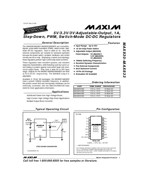
o Input Range: Up to 30V o 1A On-Chip Power Switch o Adjustable Output (MAX830) Fixed Outputs: 5V (MAX831) 3.3V (MAX832) 3V (MAX833) o 100kHz Switching Frequency o Excellent Dynamic Characteristics o Few External Components o 8mA Quiescent Current o 16-Pin SO Package o Evaluation Kit Available
__________Typical Operating Circuit
__________________Pin Configuration
TOP VIEW
INPUT 8V TO 30V 100µF VIN VSW
100µH*
OUTPUT 5V AT 1A
V IN 1 V IN 2 V IN 3
16 V SW 15 V SW 14 V SW
_______________________Applications
Distributed Power from High-Voltage Buses High-Current, High-Voltage Step-Down Applications Multiple-Output Buck Converter
MAX831
VC 10k 0.047µF SENSE
MAX6348XR中文资料
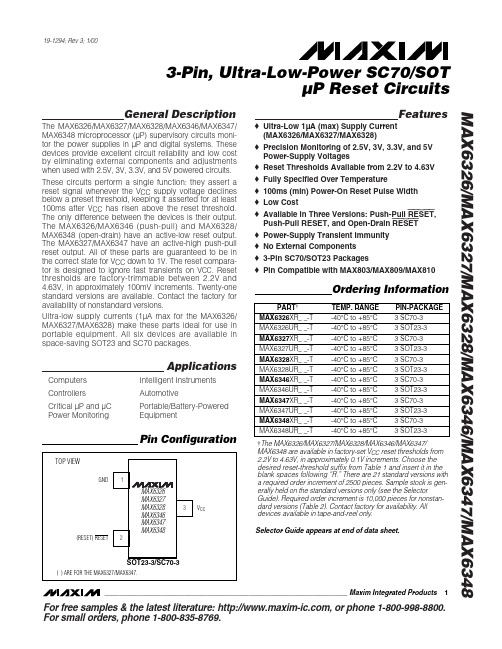
For free samples & the latest literature: , or phone 1-800-998-8800.For small orders, phone 1-800-835-8769.General DescriptionThe MAX6326/MAX6327/MAX6328/MAX6346/MAX6347/MAX6348 microprocessor (µP) supervisory circuits moni-tor the power supplies in µP and digital systems. These devices provide excellent circuit reliability and low cost by eliminating external components and adjustments when used with 2.5V, 3V, 3.3V, and 5V powered circuits.These circuits perform a single function: they assert a reset signal whenever the V CC supply voltage declines below a preset threshold, keeping it asserted for at least 100ms after V CC has risen above the reset threshold.The only difference between the devices is their output.The MAX6326/MAX6346 (push-pull) and MAX6328/MAX6348 (open-drain) have an active-low reset output.The MAX6327/MAX6347 have an active-high push-pull reset output. All of these parts are guaranteed to be in the correct state for V CC down to 1V. The reset compara-tor is designed to ignore fast transients on V CC . Reset thresholds are factory-trimmable between 2.2V and 4.63V, in approximately 100mV increments. Twenty-one standard versions are available. Contact the factory for availability of nonstandard versions.Ultra-low supply currents (1µA max for the MAX6326/MAX6327/MAX6328) make these parts ideal for use in portable equipment. All six devices are available in space-saving SOT23 and SC70 packages.ApplicationsComputers Intelligent Instruments Controllers AutomotiveCritical µP and µC Portable/Battery-Powered Power MonitoringEquipmentFeatureso Ultra-Low 1µA (max) Supply Current (MAX6326/MAX6327/MAX6328)o Precision Monitoring of 2.5V, 3V, 3.3V, and 5V Power-Supply Voltageso Reset Thresholds Available from 2.2V to 4.63V o Fully Specified Over Temperatureo 100ms (min) Power-On Reset Pulse Width o Low Costo Available in Three Versions: Push-Pull RESET ,Push-Pull RESET, and Open-Drain RESET o Power-Supply Transient Immunity o No External Componentso 3-Pin SC70/SOT23 Packageso Pin Compatible with MAX803/MAX809/MAX810MAX6326/MAX6327/MAX6328/MAX6346/MAX6347/MAX63483-Pin, Ultra-Low-Power SC70/SOTµP Reset Circuits________________________________________________________________Maxim Integrated Products 1Pin Configuration19-1294; Rev 3; 1/00†The MAX6326/MAX6327/MAX6328/MAX6346/MAX6347/MAX6348 are available in factory-set V CC reset thresholds from 2.2V to 4.63V, in approximately 0.1V increments. Choose the desired reset-threshold suffix from Table 1 and insert it in the blank spaces following “R.”There are 21 standard versions witha required order increment of 2500 pieces. Sample stock is gen-erally held on the standard versions only (see the SelectorGuide). Required order increment is 10,000 pieces for nonstan-dard versions (Table 2). Contact factory for availability. All devices available in tape-and-reel only.Selector Guide appears at end of data sheet.M A X 6326/M A X 6327/M A X 6328/M A X 6346/M A X 6347/M A X 63483-Pin, Ultra-Low-Power SC70/SOT µP Reset Circuits 2_______________________________________________________________________________________ABSOLUTE MAXIMUM RATINGSELECTRICAL CHARACTERISTICS(V CC = full range, T A = -40°C to +85°C, unless otherwise noted. Typical values are at T A = +25°C and V CC = 3V.) (Note 1)Stresses beyond those listed under “Absolute Maximum Ratings” may cause permanent damage to the device. These are stress ratings only, and functional operation of the device at these or any other conditions beyond those indicated in the operational sections of the specifications is not implied. Exposure to absolute maximum rating conditions for extended periods may affect device reliability.Terminal Voltage (with respect to GND)V CC ...........................................................................-0.3V to +6V RESET, RESET (push-pull).........................-0.3V to (V CC + 0.3V)RESET (open drain)..................................................-0.3V to +6V Input Current (V CC ).............................................................20mA Output Current (RESET, RESET ).........................................20mA Rate of Rise (V CC )...........................................................100V/µsContinuous Power Dissipation (T A = +70°C)3-Pin SC70 (derate 2.7mW/°C above +70°C)...............174mW 3-Pin SOT23 (derate 4mW/°C above +70°C)................320mW Operating Temperature Range ...........................-40°C to +85°C Storage Temperature Range.............................-65°C to +150°C Lead Temperature (soldering, 10s).................................+300°CNote 1:Overtemperature limits are guaranteed by design and not production tested.MAX6326/MAX6327/MAX6328/MAX6346/MAX6347/MAX63483-Pin, Ultra-Low-Power SC70/SOTµP Reset Circuits_______________________________________________________________________________________3__________________________________________Typical Operating Characteristics(T A = +25°C, unless otherwise noted.)00.30.20.10.40.50.60.70.80.91.0-400-2020406080SUPPLY CURRENT vs. TEMPERATURE TEMPERATURE (°C)S U P P L Y C U R R E N T(µA)050100150200-400-2020406080POWER-DOWN RESET DELAY vs. TEMPERATURE TEMPERATURE (°C)R E S E T D E L A Y(µs)130150140160170180190200210-400-2020406080POWER-UP RESET TIMEOUT vs. TEMPERATURE M A X6326-03TEMPERATURE (°C)P O W E R-U P R E S E T T I M E O U T(m s)500011001000MAXIMUM TRANSIENT DURATION vs. RESET THRESHOLD OVERDRIVE (SC70)100300400200M A X6326-04RESET THRESHOLD OVERDRIVE,V TH - V CC (mV)M A X I M U M T R A N S I E N T D U R A T I O N(µs)10______________________________________________________________Pin DescriptionM A X 6326/M A X 6327/M A X 6328/M A X 6346/M A X 6347/M A X 63483-Pin, Ultra-Low-Power SC70/SOT µP Reset Circuits 4___________________________________________________________________________________________________Applications InformationInterfacing to µPs with Bidirectional Reset PinsSince the RESET output on the MAX6328/MAX6348 is open drain, these devices interface easily with micro-processors (µPs) that have bidirectional reset pins,such as the Motorola 68HC11. Connecting the µP supervisor’s RESET output directly to the microcon-troller’s (µC’s) RESET pin with a single pull-up resistor allows either device to assert reset (Figure 1).Negative-Going V CC TransientsIn addition to issuing a reset to the µP during power-up,power-down, and brownout conditions, these devices are relatively immune to short-duration, negative-going V CC transients (glitches).The Typical Operating Characteristics show the Maxi-mum Transient Duration vs. Reset Threshold Overdrive graph, for which reset pulses are not generated. The graph shows the maximum pulse width that a negative-going V CC transient may typically have when issuing a reset signal. As the amplitude of the transient increas-es, the maximum allowable pulse width decreases.Figure 1. Interfacing to µPs with Bidirectional Reset PinsTable 1. Factory-Trimmed Reset Thresholds ‡‡Factory-trimmed reset thresholds are available in approximately 100mV increments with a 1.5% room-temperature variance.MAX6326/MAX6327/MAX6328/MAX6346/MAX6347/MAX63483-Pin, Ultra-Low-Power SC70/SOTµP Reset Circuits_______________________________________________________________________________________5Table 1. Factory-Trimmed Reset Thresholds‡(continued)‡Factory-trimmed reset thresholds are available in approximately 100mV increments with a 1.5% room-temperature variance.Table 2. Device Marking Codes and Minimum Order IncrementsM A X 6326/M A X 6327/M A X 6328/M A X 6346/M A X 6347/M A X 63483-Pin, Ultra-Low-Power SC70/SOT µP Reset Circuits 6__________________________________________________________________________________________________________Chip InformationTRANSISTOR COUNT: 419Table 2. Device Marking Codes and Minimum Order Increments (continued)Selector Guide(standard versions*)*Sample stock is generally held on all standard versions.________________________________________________________Package InformationMAX6326/MAX6327/MAX6328/MAX6346/MAX6347/MAX63483-Pin, Ultra-Low-Power SC70/SOTµP Reset Circuits_______________________________________________________________________________________7M A X 6326/M A X 6327/M A X 6328/M A X 6346/M A X 6347/M A X 63483-Pin, Ultra-Low-Power SC70/SOT µP Reset Circuits Maxim cannot assume responsibility for use of any circuitry other than circuitry entirely embodied in a Maxim product. No circuit patent licenses are implied. Maxim reserves the right to change the circuitry and specifications without notice at any time.8_____________________Maxim Integrated Products, 120 San Gabriel Drive, Sunnyvale, CA 94086 408-737-7600©2000 Maxim Integrated ProductsPrinted USAis a registered trademark of Maxim Integrated Products.Package Information (continued)。
MAX13085EESA-T中文资料

General DescriptionThe MAX13080E–MAX13089E +5.0V, ±15kV ESD-protect-ed, RS-485/RS-422 transceivers feature one driver and one receiver. These devices include fail-safe circuitry,guaranteeing a logic-high receiver output when receiver inputs are open or shorted. The receiver outputs a logic-high if all transmitters on a terminated bus are disabled (high impedance). The MAX13080E–MAX13089E include a hot-swap capability to eliminate false transitions on the bus during power-up or hot insertion.The MAX13080E/MAX13081E/MAX13082E feature reduced slew-rate drivers that minimize EMI and reduce reflections caused by improperly terminated cables, allowing error-free data transmission up to 250kbps. The MAX13083E/MAX13084E/MAX13085E also feature slew-rate-limited drivers but allow transmit speeds up to 500kbps. The MAX13086E/MAX13087E/MAX13088E driver slew rates are not limited, making transmit speeds up to 16Mbps possible. The MAX13089E slew rate is pin selectable for 250kbps,500kbps, and 16Mbps.The MAX13082E/MAX13085E/MAX13088E are intended for half-duplex communications, and the MAX13080E/MAX13081E/MAX13083E/MAX13084E/MAX13086E/MAX13087E are intended for full-duplex communica-tions. The MAX13089E is selectable for half-duplex or full-duplex operation. It also features independently programmable receiver and transmitter output phase through separate pins.The MAX13080E–MAX13089E transceivers draw 1.2mA of supply current when unloaded or when fully loaded with the drivers disabled. All devices have a 1/8-unit load receiver input impedance, allowing up to 256transceivers on the bus.The MAX13080E/MAX13083E/MAX13086E/MAX13089E are available in 14-pin PDIP and 14-pin SO packages.The MAX13081E/MAX13082E/MAX13084E/MAX13085E/MAX13087E/MAX13088E are available in 8-pin PDIP and 8-pin SO packages. The devices operate over the com-mercial, extended, and automotive temperature ranges.ApplicationsUtility Meters Lighting Systems Industrial Control Telecom Security Systems Instrumentation ProfibusFeatures♦+5.0V Operation♦Extended ESD Protection for RS-485/RS-422 I/O Pins±15kV Human Body Model ♦True Fail-Safe Receiver While Maintaining EIA/TIA-485 Compatibility ♦Hot-Swap Input Structures on DE and RE ♦Enhanced Slew-Rate Limiting Facilitates Error-Free Data Transmission(MAX13080E–MAX13085E/MAX13089E)♦Low-Current Shutdown Mode (Except MAX13081E/MAX13084E/MAX13087E)♦Pin-Selectable Full-/Half-Duplex Operation (MAX13089E)♦Phase Controls to Correct for Twisted-Pair Reversal (MAX13089E)♦Allow Up to 256 Transceivers on the Bus ♦Available in Industry-Standard 8-Pin SO PackageMAX13080E–MAX13089E+5.0V , ±15kV ESD-Protected, Fail-Safe, Hot-Swap, RS-485/RS-422 Transceivers________________________________________________________________Maxim Integrated Products 1Ordering Information19-3590; Rev 1; 4/05For pricing, delivery, and ordering information,please contact Maxim/Dallas Direct!at 1-888-629-4642, or visit Maxim’s website at .Selector Guide, Pin Configurations, and Typical Operating Circuits appear at end of data sheet.Ordering Information continued at end of data sheet.M A X 13080E –M A X 13089E+5.0V , ±15kV ESD-Protected, Fail-Safe, Hot-Swap, RS-485/RS-422 Transceivers 2_______________________________________________________________________________________ABSOLUTE MAXIMUM RATINGSDC ELECTRICAL CHARACTERISTICS(V CC = +5.0V ±10%, T A = T MIN to T MAX , unless otherwise noted. Typical values are at V CC = +5.0V and T A = +25°C.) (Note 1)Stresses beyond those listed under “Absolute Maximum Ratings” may cause permanent damage to the device. These are stress ratings only, and functional operation of the device at these or any other conditions beyond those indicated in the operational sections of the specifications is not implied. Exposure to absolute maximum rating conditions for extended periods may affect device reliability.(All Voltages Referenced to GND)Supply Voltage (V CC ).............................................................+6V Control Input Voltage (RE , DE, SLR,H/F , TXP, RXP)......................................................-0.3V to +6V Driver Input Voltage (DI)...........................................-0.3V to +6V Driver Output Voltage (Z, Y, A, B).............................-8V to +13V Receiver Input Voltage (A, B)....................................-8V to +13V Receiver Input VoltageFull Duplex (A, B)..................................................-8V to +13V Receiver Output Voltage (RO)....................-0.3V to (V CC + 0.3V)Driver Output Current.....................................................±250mAContinuous Power Dissipation (T A = +70°C)8-Pin SO (derate 5.88mW/°C above +70°C).................471mW 8-Pin Plastic DIP (derate 9.09mW/°C above +70°C).....727mW 14-Pin SO (derate 8.33mW/°C above +70°C)...............667mW 14-Pin Plastic DIP (derate 10.0mW/°C above +70°C)...800mW Operating Temperature RangesMAX1308_EC_ _.................................................0°C to +75°C MAX1308_EE_ _..............................................-40°C to +85°C MAX1308_EA_ _............................................-40°C to +125°C Junction Temperature......................................................+150°C Storage Temperature Range.............................-65°C to +150°C Lead Temperature (soldering, 10s).................................+300°CMAX13080E–MAX13089E+5.0V , ±15kV ESD-Protected, Fail-Safe, Hot-Swap, RS-485/RS-422 Transceivers_______________________________________________________________________________________3DC ELECTRICAL CHARACTERISTICS (continued)(V CC = +5.0V ±10%, T A = T MIN to T MAX , unless otherwise noted. Typical values are at V CC = +5.0V and T A = +25°C.) (Note 1)M A X 13080E –M A X 13089E+5.0V , ±15kV ESD-Protected, Fail-Safe, Hot-Swap, RS-485/RS-422 Transceivers 4_______________________________________________________________________________________DRIVER SWITCHING CHARACTERISTICSMAX13080E/MAX13081E/MAX13082E/MAX13089E WITH SRL = UNCONNECTED (250kbps)(V CC = +5.0V ±10%, T A = T MIN to T MAX , unless otherwise noted. Typical values are at V CC = +5.0V and T A = +25°C.)RECEIVER SWITCHING CHARACTERISTICSMAX13080E/MAX13081E/MAX13082E/MAX13089E WITH SRL = UNCONNECTED (250kbps)(V CC = +5.0V ±10%, T A = T MIN to T MAX , unless otherwise noted. Typical values are at V CC = +5.0V and T A = +25°C.)MAX13080E–MAX13089E+5.0V , ±15kV ESD-Protected, Fail-Safe, Hot-Swap, RS-485/RS-422 Transceivers_______________________________________________________________________________________5DRIVER SWITCHING CHARACTERISTICSMAX13083E/MAX13084E/MAX13085E/MAX13089E WITH SRL = V CC (500kbps)(V CC = +5.0V ±10%, T A = T MIN to T MAX , unless otherwise noted. Typical values are at V CC = +5.0V and T A = +25°C.)RECEIVER SWITCHING CHARACTERISTICSMAX13083E/MAX13084E/MAX13085E/MAX13089E WITH SRL = V CC (500kbps)(V CC = +5.0V ±10%, T A = T MIN to T MAX , unless otherwise noted. Typical values are at V CC = +5.0V and T A = +25°C.)M A X 13080E –M A X 13089E+5.0V , ±15kV ESD-Protected, Fail-Safe, Hot-Swap, RS-485/RS-422 Transceivers 6_______________________________________________________________________________________DRIVER SWITCHING CHARACTERISTICSMAX13086E/MAX13087E/MAX13088E/MAX13089E WITH SRL = GND (16Mbps)(V CC = +5.0V ±10%, T A = T MIN to T MAX , unless otherwise noted. Typical values are at V CC = +5.0V and T A = +25°C.)RECEIVER SWITCHING CHARACTERISTICSMAX13086E/MAX13087E/MAX13088E/MAX13089E WITH SRL = GND (16Mbps)(V CC = +5.0V ±10%, T A = T MIN to T MAX , unless otherwise noted. Typical values are at V CC = +5.0V and T A = +25°C.)Note 2:∆V OD and ∆V OC are the changes in V OD and V OC , respectively, when the DI input changes state.Note 3:The short-circuit output current applies to peak current just prior to foldback current limiting. The short-circuit foldback outputcurrent applies during current limiting to allow a recovery from bus contention.MAX13080E–MAX13089E+5.0V , ±15kV ESD-Protected, Fail-Safe, Hot-Swap, RS-485/RS-422 Transceivers_______________________________________________________________________________________70.800.901.501.101.001.201.301.401.60-40-10520-253550958011065125SUPPLY CURRENT vs. TEMPERATURETEMPERATURE (°C)S U P P L Y C U R R E N T (m A )0201040305060021345OUTPUT CURRENTvs. RECEIVER OUTPUT-HIGH VOLTAGEM A X 13080E -89E t o c 02OUTPUT HIGH VOLTAGE (V)O U T P U T C U R R E N T (m A )20104030605070021345OUTPUT CURRENTvs. RECEIVER OUTPUT-LOW VOLTAGEM A X 13080E -89E t o c 03OUTPUT LOW VOLTAGE (V)O U T P U T C U R R E N T (m A )4.04.44.24.84.65.25.05.4RECEIVER OUTPUT-HIGH VOLTAGEvs. TEMPERATURETEMPERATURE (°C)O U T P U T H I G H V O L T A G E (V )-40-10520-2535509580110651250.10.70.30.20.40.50.60.8RECEIVER OUTPUT-LOW VOLTAGEvs. TEMPERATURETEMPERATURE (°C)O U T P U T L O W V O L T A G E (V )-40-10520-25355095801106512502040608010012014016012345DRIVER DIFFERENTIAL OUTPUT CURRENT vs. DIFFERENTIAL OUTPUT VOLTAGEDIFFERENTIAL OUTPUT VOLTAGE (V)D I F FE R E N T I A L O U T P U T C U R R E N T (m A )2.02.82.43.63.24.44.04.8DRIVER DIFFERENTIAL OUTPUT VOLTAGE vs. TEMPERATURED I F FE R E N T I A L O U T P U T V O L T A G E (V )-40-10520-253550958011065125TEMPERATURE (°C)40201008060120140180160200-7-5-4-6-3-2-1012354OUTPUT CURRENT vs. TRANSMITTEROUTPUT-HIGH VOLTAGEOUTPUT HIGH VOLTAGE (V)O U T P U T C U R R E N T (m A )60402080100120140160180200042681012OUTPUT CURRENT vs. TRANSMITTEROUTPUT-LOW VOLTAGEOUTPUT-LOW VOLTAGE (V)O U T P U T C U R R E N T (m A )Typical Operating Characteristics(V CC = +5.0V, T A = +25°C, unless otherwise noted.)M A X 13080E –M A X 13089E+5.0V , ±15kV ESD-Protected, Fail-Safe, Hot-Swap, RS-485/RS-422 Transceivers 8_______________________________________________________________________________________21543679810SHUTDOWN CURRENT vs. TEMPERATUREM A X 13080E -89E t o c 10S H U T D O W N C U R R E N T (µA )-40-10520-253550958011065125TEMPERATURE (°C)600800700100090011001200DRIVER PROPAGATION DELAY vs. TEMPERATURE (250kbps)D R I VE R P R O P A G A T I O N D E L A Y (n s )-40-10520-253550958011065125TEMPERATURE (°C)300400350500450550600DRIVER PROPAGATION DELAY vs. TEMPERATURE (500kbps)D R I VE R P R O P A G A T I O N D E L A Y (n s )-40-10520-253550958011065125TEMPERATURE (°C)1070302040506080DRIVER PROPAGATION DELAY vs. TEMPERATURE (16Mbps)D R I VE R P R O P A G A T I O N D E L A Y (n s )-40-10520-253550958011065125TEMPERATURE (°C)40201008060120140160180RECEIVER PROPAGATION DELAYvs. TEMPERATURE (250kpbs AND 500kbps)R E C E I V E R P R O P A G A T I O N D E L A Y (n s )-40-10520-253550958011065125TEMPERATURE (°C)40201008060120140160180RECEIVER PROPAGATION DELAYvs. TEMPERATURE (16Mbps)R EC E I V E R P R O P A G AT I O N D E L A Y (n s )-40-10520-253550958011065125TEMPERATURE (°C)2µs/div DRIVER PROPAGATION DELAY (250kbps)DI 2V/divV Y - V Z 5V/divR L = 100Ω200ns/divRECEIVER PROPAGATION DELAY(250kbps AND 500kbps)V A - V B 5V/divRO 2V/divTypical Operating Characteristics (continued)(V CC = +5.0V, T A = +25°C, unless otherwise noted.)MAX13080E–MAX13089E+5.0V , ±15kV ESD-Protected, Fail-Safe, Hot-Swap, RS-485/RS-422 Transceivers_______________________________________________________________________________________9Test Circuits and Waveforms400ns/divDRIVER PROPAGATION DELAY (500kbps)DI 2V/divR L = 100ΩV Y - V Z 5V/div10ns/div DRIVER PROPAGATION DELAY (16Mbps)DI 2V/divR L = 100ΩV Y 2V/divV Z 2V/div40ns/divRECEIVER PROPAGATION DELAY (16Mbps)V B 2V/divR L = 100ΩRO 2V/divV A 2V/divTypical Operating Characteristics (continued)(V CC = +5.0V, T A = +25°C, unless otherwise noted.)Figure 2. Driver Timing Test CircuitM A X 13080E –M A X 13089E+5.0V , ±15kV ESD-Protected, Fail-Safe, Hot-Swap, RS-485/RS-422 Transceivers 10______________________________________________________________________________________Test Circuits and Waveforms (continued)Figure 4. Driver Enable and Disable Times (t DHZ , t DZH , t DZH(SHDN))DZL DLZ DLZ(SHDN)MAX13080E–MAX13089E+5.0V , ±15kV ESD-Protected, Fail-Safe, Hot-Swap, RS-485/RS-422 TransceiversTest Circuits and Waveforms (continued)Figure 6. Receiver Propagation Delay Test CircuitM A X 13080E –M A X 13089E+5.0V , ±15kV ESD-Protected, Fail-Safe, Hot-Swap, RS-485/RS-422 TransceiversMAX13080E–MAX13089E+5.0V , ±15kV ESD-Protected, Fail-Safe, Hot-Swap, RS-485/RS-422 TransceiversMAX13080E/MAX13083E/MAX13086EMAX13081E/MAX13084E/MAX13086E/MAX13087EFunction TablesM A X 13080E –M A X 13089E+5.0V , ±15kV ESD-Protected, Fail-Safe, Hot-Swap, RS-485/RS-422 Transceivers MAX13082E/MAX13085E/MAX13088EFunction Tables (continued)MAX13089EDetailed Description The MAX13080E–MAX13089E high-speed transceivers for RS-485/RS-422 communication contain one driver and one receiver. These devices feature fail-safe circuit-ry, which guarantees a logic-high receiver output when the receiver inputs are open or shorted, or when they are connected to a terminated transmission line with all dri-vers disabled (see the Fail-Safe section). The MAX13080E/MAX13082E/MAX13083E/MAX13085E/ MAX13086E/MAX13088E/MAX13089E also feature a hot-swap capability allowing line insertion without erroneous data transfer (see the Hot Swap Capability section). The MAX13080E/MAX13081E/MAX13082E feature reduced slew-rate drivers that minimize EMI and reduce reflec-tions caused by improperly terminated cables, allowing error-free data transmission up to 250kbps. The MAX13083E/MAX13084E/MAX13085E also offer slew-rate limits allowing transmit speeds up to 500kbps. The MAX13086E/MAX13087E/MAX13088Es’ driver slew rates are not limited, making transmit speeds up to 16Mbps possible. The MAX13089E’s slew rate is selectable between 250kbps, 500kbps, and 16Mbps by driving a selector pin with a three-state driver.The MAX13082E/MAX13085E/MAX13088E are half-duplex transceivers, while the MAX13080E/MAX13081E/ MAX13083E/MAX13084E/MAX13086E/MAX13087E are full-duplex transceivers. The MAX13089E is selectable between half- and full-duplex communication by driving a selector pin (H/F) high or low, respectively.All devices operate from a single +5.0V supply. Drivers are output short-circuit current limited. Thermal-shutdown circuitry protects drivers against excessive power dissi-pation. When activated, the thermal-shutdown circuitry places the driver outputs into a high-impedance state.Receiver Input Filtering The receivers of the MAX13080E–MAX13085E, and the MAX13089E when operating in 250kbps or 500kbps mode, incorporate input filtering in addition to input hysteresis. This filtering enhances noise immunity with differential signals that have very slow rise and fall times. Receiver propagation delay increases by 25% due to this filtering.Fail-Safe The MAX13080E family guarantees a logic-high receiver output when the receiver inputs are shorted or open, or when they are connected to a terminated transmission line with all drivers disabled. This is done by setting the receiver input threshold between -50mV and -200mV. If the differential receiver input voltage (A - B) is greater than or equal to -50mV, RO is logic-high. If (A - B) is less than or equal to -200mV, RO is logic-low. In the case of a terminated bus with all transmitters disabled, the receiv-er’s differential input voltage is pulled to 0V by the termi-nation. With the receiver thresholds of the MAX13080E family, this results in a logic-high with a 50mV minimumnoise margin. Unlike previous fail-safe devices, the-50mV to -200mV threshold complies with the ±200mVEIA/TIA-485 standard.Hot-Swap Capability (Except MAX13081E/MAX13084E/MAX13087E)Hot-Swap InputsWhen circuit boards are inserted into a hot or powered backplane, differential disturbances to the data buscan lead to data errors. Upon initial circuit board inser-tion, the data communication processor undergoes itsown power-up sequence. During this period, the processor’s logic-output drivers are high impedanceand are unable to drive the DE and RE inputs of these devices to a defined logic level. Leakage currents up to±10µA from the high-impedance state of the proces-sor’s logic drivers could cause standard CMOS enableinputs of a transceiver to drift to an incorrect logic level. Additionally, parasitic circuit board capacitance couldcause coupling of V CC or GND to the enable inputs. Without the hot-swap capability, these factors could improperly enable the transceiver’s driver or receiver.When V CC rises, an internal pulldown circuit holds DElow and RE high. After the initial power-up sequence,the pulldown circuit becomes transparent, resetting thehot-swap tolerable input.Hot-Swap Input CircuitryThe enable inputs feature hot-swap capability. At theinput there are two NMOS devices, M1 and M2 (Figure 9). When V CC ramps from zero, an internal 7µstimer turns on M2 and sets the SR latch, which alsoturns on M1. Transistors M2, a 1.5mA current sink, andM1, a 500µA current sink, pull DE to GND through a5kΩresistor. M2 is designed to pull DE to the disabledstate against an external parasitic capacitance up to100pF that can drive DE high. After 7µs, the timer deactivates M2 while M1 remains on, holding DE low against three-state leakages that can drive DE high. M1 remains on until an external source overcomes the required input current. At this time, the SR latch resetsand M1 turns off. When M1 turns off, DE reverts to a standard, high-impedance CMOS input. Whenever V CCdrops below 1V, the hot-swap input is reset.For RE there is a complementary circuit employing two PMOS devices pulling RE to V CC. MAX13080E–MAX13089E+5.0V, ±15kV ESD-Protected, Fail-Safe, Hot-Swap, RS-485/RS-422 TransceiversM A X 13080E –M A X 13089EMAX13089E ProgrammingThe MAX13089E has several programmable operating modes. Transmitter rise and fall times are programma-ble, resulting in maximum data rates of 250kbps,500kbps, and 16Mbps. To select the desired data rate,drive SRL to one of three possible states by using a three-state driver: V CC , GND, or unconnected. F or 250kbps operation, set the three-state device in high-impedance mode or leave SRL unconnected. F or 500kbps operation, drive SRL high or connect it to V CC .F or 16Mbps operation, drive SRL low or connect it to GND. SRL can be changed during operation without interrupting data communications.Occasionally, twisted-pair lines are connected backward from normal orientation. The MAX13089E has two pins that invert the phase of the driver and the receiver to cor-rect this problem. F or normal operation, drive TXP and RXP low, connect them to ground, or leave them uncon-nected (internal pulldown). To invert the driver phase,drive TXP high or connect it to V CC . To invert the receiver phase, drive RXP high or connect it to V CC . Note that the receiver threshold is positive when RXP is high.The MAX13089E can operate in full- or half-duplex mode. Drive H/F low, leave it unconnected (internal pulldown), or connect it to GND for full-duplex opera-tion. Drive H/F high for half-duplex operation. In full-duplex mode, the pin configuration of the driver and receiver is the same as that of a MAX13080E. In half-duplex mode, the receiver inputs are internally connect-ed to the driver outputs through a resistor-divider. This effectively changes the function of the device’s outputs.Y becomes the noninverting driver output and receiver input, Z becomes the inverting driver output and receiver input. In half-duplex mode, A and B are still connected to ground through an internal resistor-divider but they are not internally connected to the receiver.±15kV ESD ProtectionAs with all Maxim devices, ESD-protection structures are incorporated on all pins to protect against electro-static discharges encountered during handling and assembly. The driver outputs and receiver inputs of the MAX13080E family of devices have extra protection against static electricity. Maxim’s engineers have devel-oped state-of-the-art structures to protect these pins against ESD of ±15kV without damage. The ESD struc-tures withstand high ESD in all states: normal operation,shutdown, and powered down. After an ESD event, the MAX13080E–MAX13089E keep working without latchup or damage.ESD protection can be tested in various ways. The transmitter outputs and receiver inputs of the MAX13080E–MAX13089E are characterized for protec-tion to the following limits:•±15kV using the Human Body Model•±6kV using the Contact Discharge method specified in IEC 61000-4-2ESD Test ConditionsESD performance depends on a variety of conditions.Contact Maxim for a reliability report that documents test setup, test methodology, and test results.Human Body ModelFigure 10a shows the Human Body Model, and Figure 10b shows the current waveform it generates when dis-charged into a low impedance. This model consists of a 100pF capacitor charged to the ESD voltage of interest,which is then discharged into the test device through a 1.5k Ωresistor.IEC 61000-4-2The IEC 61000-4-2 standard covers ESD testing and performance of finished equipment. However, it does not specifically refer to integrated circuits. The MAX13080E family of devices helps you design equip-ment to meet IEC 61000-4-2, without the need for addi-tional ESD-protection components.+5.0V , ±15kV ESD-Protected, Fail-Safe, Hot-Swap, RS-485/RS-422 TransceiversThe major difference between tests done using the Human Body Model and IEC 61000-4-2 is higher peak current in IEC 61000-4-2 because series resistance is lower in the IEC 61000-4-2 model. Hence, the ESD with-stand voltage measured to IEC 61000-4-2 is generally lower than that measured using the Human Body Model. Figure 10c shows the IEC 61000-4-2 model, and Figure 10d shows the current waveform for IEC 61000-4-2 ESD Contact Discharge test.Machine Model The machine model for ESD tests all pins using a 200pF storage capacitor and zero discharge resis-tance. The objective is to emulate the stress caused when I/O pins are contacted by handling equipment during test and assembly. Of course, all pins require this protection, not just RS-485 inputs and outputs.Applications Information256 Transceivers on the BusThe standard RS-485 receiver input impedance is 12kΩ(1-unit load), and the standard driver can drive up to 32-unit loads. The MAX13080E family of transceivers has a1/8-unit load receiver input impedance (96kΩ), allowingup to 256 transceivers to be connected in parallel on one communication line. Any combination of these devices,as well as other RS-485 transceivers with a total of 32-unit loads or fewer, can be connected to the line.Reduced EMI and ReflectionsThe MAX13080E/MAX13081E/MAX13082E feature reduced slew-rate drivers that minimize EMI and reduce reflections caused by improperly terminated cables, allowing error-free data transmission up to250kbps. The MAX13083E/MAX13084E/MAX13085Eoffer higher driver output slew-rate limits, allowing transmit speeds up to 500kbps. The MAX13089E withSRL = V CC or unconnected are slew-rate limited. WithSRL unconnected, the MAX13089E error-free data transmission is up to 250kbps. With SRL connected toV CC,the data transmit speeds up to 500kbps. MAX13080E–MAX13089E+5.0V, ±15kV ESD-Protected, Fail-Safe, Hot-Swap, RS-485/RS-422 TransceiversM A X 13080E –M A X 13089ELow-Power Shutdown Mode (Except MAX13081E/MAX13084E/MAX13087E)Low-power shutdown mode is initiated by bringing both RE high and DE low. In shutdown, the devices typically draw only 2.8µA of supply current.RE and DE can be driven simultaneously; the devices are guaranteed not to enter shutdown if RE is high and DE is low for less than 50ns. If the inputs are in this state for at least 700ns, the devices are guaranteed to enter shutdown.Enable times t ZH and t ZL (see the Switching Characteristics section) assume the devices were not in a low-power shutdown state. Enable times t ZH(SHDN)and t ZL(SHDN)assume the devices were in shutdown state. It takes drivers and receivers longer to become enabled from low-power shutdown mode (t ZH(SHDN), t ZL(SHDN))than from driver/receiver-disable mode (t ZH , t ZL ).Driver Output ProtectionTwo mechanisms prevent excessive output current and power dissipation caused by faults or by bus contention.The first, a foldback current limit on the output stage,provides immediate protection against short circuits over the whole common-mode voltage range (see the Typical Operating Characteristics ). The second, a thermal-shut-down circuit, forces the driver outputs into a high-imped-ance state if the die temperature exceeds +175°C (typ).Line LengthThe RS-485/RS-422 standard covers line lengths up to 4000ft. F or line lengths greater than 4000ft, use the repeater application shown in Figure 11.Typical ApplicationsThe MAX13082E/MAX13085E/MAX13088E/MAX13089E transceivers are designed for bidirectional data commu-nications on multipoint bus transmission lines. F igures 12 and 13 show typical network applications circuits. To minimize reflections, terminate the line at both ends in its characteristic impedance, and keep stub lengths off the main line as short as possible. The slew-rate-lim-ited MAX13082E/MAX13085E and the two modes of the MAX13089E are more tolerant of imperfect termination.Chip InformationTRANSISTOR COUNT: 1228PROCESS: BiCMOS+5.0V , ±15kV ESD-Protected, Fail-Safe, Hot-Swap, RS-485/RS-422 TransceiversFigure 11. Line Repeater for MAX13080E/MAX13081E/MAX13083E/MAX13084E/MAX13086E/MAX13087E/MAX13089E in Full-Duplex Mode+5.0V, ±15kV ESD-Protected, Fail-Safe, Hot-Swap, RS-485/RS-422 TransceiversMAX13080E–MAX13089EM A X 13080E –M A X 13089E+5.0V , ±15kV ESD-Protected, Fail-Safe, Hot-Swap, RS-485/RS-422 TransceiversPin Configurations and Typical Operating CircuitsMAX13080E–MAX13089E+5.0V , ±15kV ESD-Protected, Fail-Safe, Hot-Swap, RS-485/RS-422 Transceivers______________________________________________________________________________________21Pin Configurations and Typical Operating Circuits (continued)M A X 13080E –M A X 13089E+5.0V , ±15kV ESD-Protected, Fail-Safe, Hot-Swap, RS-485/RS-422 Transceivers 22______________________________________________________________________________________Ordering Information (continued)MAX13080E–MAX13089E+5.0V , ±15kV ESD-Protected, Fail-Safe, Hot-Swap, RS-485/RS-422 Transceivers______________________________________________________________________________________23Package Information (continued)(The package drawing(s) in this data sheet may not reflect the most current specifications. For the latest package outline information,go to /packages .)。
Datasheet MLX90614 中文 数据手册 rev008

单区视场和双区视场 TO-39 封装 红外温度传感器
特性和优点
尺寸小,成本低 易集成 在极宽温度范围内工作,带出厂校准: 传感器工作温度范围:-40…+125˚C 被测目标温度范围:-70…+380˚C Ta 和 To 在 0 到 50° C 时,测量精度可达 0.5° C 高(医疗)精度校准 测量值分辨率 0.02° C 单区视场和双区视场可选 SMBus 兼容数字接口 可配置 PWM 连续输出 3V 或 5V 供电,也可使用 8…16V 供电调制 支持睡眠模式 适合不同应用领域的多种封装方式和测试方式 车用级别标准
3901090614 Rev 008
第 2ห้องสมุดไป่ตู้/ 52 页
数据手册 2013/2/28
MLX90614 系列
单区视场和双区视场 TO-39 封装 红外温度传感器
3 目录
1 功能图 ........................................................................................................................................................................................................ 1 2 概述 ......................................................................................................................................................................
Analog Devices ADM6384YKS29D3Z-R7 微处理器监测电路说明书

ADM6384YKS29D3Z-R7ADM6384YKS23D3Z-R7Microprocessor SupervisoryRev. CInformation furnished by Analog Devices is believed to be accurate and reliable. However, noresponsibility is assumed by Analog Devices for its use, nor for any infringements of patents or other rights of third parties that may result from its use. Specifications subject to change without notice. No license is granted by implication or otherwise under any patent or patent rights of Analog Devices. T rademarks and registered trademarks are the property of their respective owners. One Technology Way, P.O. Box 9106, Norwood, M A 02062-9106, U.S.A. Tel: 781.329.4700 Fax: 781.461.3113 ©2005–2011 Analog Devices, Inc. All rights reserved.FEATURESPrecision power supply monitoring31 reset threshold options: 1.58 V to 5.0 VFour reset timeouts: 1 ms, 20 ms, 140 ms, and 1120 ms Manual reset inputReset output stagePush-pull active-lowGuaranteed reset output valid to V CC = 1 VPower supply glitch immunitySpecified over the −40°C to +125°C temperature range4-lead SC70 packageAPPLICATIONSMicroprocessor systemsComputersControllersIntelligent instrumentsPortable equipmentGENERAL DESCRIPTIONThe ADM6384 is a supervisory circuit that monitors power supply voltage levels in microprocessor-based systems. A power-on reset signal is generated when the supply voltage rises to a preset threshold level. The debounced manual reset input of the ADM6384 can be used to initiate a reset by means of an external push button or logic signal.The part is available in a choice of 31 reset threshold options, from 1.58 V to 5.0 V. The minimum reset timeout periods are 1 ms, 20 ms, 140 ms, and 1120 ms.The ADM6384 is available in a 4-lead SC70 package and typi-cally consumes only 7 µA, making it suitable for use in low power, portable applications. FUNCTIONAL BLOCK DIAGRAMSFigure 1.535-2Figure 2.ADM6384Rev. C | Page 2 of 12TABLE OF CONTENTSFeatures .............................................................................................. 1 Applications ....................................................................................... 1 General Description ......................................................................... 1 Functional Block Diagrams ............................................................. 1 Revision History ............................................................................... 2 Specifications ..................................................................................... 3 Absolute Maximum Ratings ............................................................ 5 ESD Caution .................................................................................. 5 Pin Configuration and Function Descriptions ............................. 6 Typical Performance Characteristics ..............................................7 Circuit Description............................................................................9 Reset Output ..................................................................................9 Manual Reset Input .......................................................................9 Applications Information .............................................................. 10 Negative-Going V CC Transients ................................................ 10 Ensuring Reset Valid to V CC = 0 V ........................................... 10 Outline Dimensions ....................................................................... 11 Ordering Guide .. (11)REVISION HISTORY4/11—Rev. B to Rev. CUpdated Outline Dimensions ....................................................... 11 Changes to Ordering Guide . (11)7/08—Rev. A to Rev. BChanges to Figure 5, Figure 8, and Figure 9.................................. 7 Changes to Figure 10 ........................................................................ 8 Changes to Figure 15 ...................................................................... 11 Changes to Ordering Guide . (11)1/07—Rev. 0 to Rev. AUpdated Format .................................................................. U niversal Changes to Specifications Table ...................................................... 3 Updated Outline Dimensions ....................................................... 11 Changes to Ordering Guide . (11)7/05—Revision 0: Initial VersionSPECIFICATIONSV CC = full operating range, T A = −40°C to +125°C, unless otherwise noted.Rev. C | Page 3 of 121 T A = 25°C only.Rev. C | Page 4 of 12Rev. C | Page 5 of 12ABSOLUTE MAXIMUM RATINGST A = 25°C, unless otherwise noted.Stresses above those listed under Absolute Maximum Ratings may cause permanent damage to the device. This is a stress rating only; functional operation of the device at these or any other conditions above those indicated in the operationalsection of this specification is not implied. Exposure to absolute maximum rating conditions for extended periods may affect device reliability.Rev. C | Page 6 of 12PIN CONFIGURATION AND FUNCTION DESCRIPTIONSGNDRESET 05305-003Figure 3. Pin ConfigurationRev. C | Page 7 of 12TYPICAL PERFORMANCE CHARACTERISTICS05305-004TEMPERATURE (°C)120–40–2020406080100I C C (µA )10.09.57.57.06.59.08.58.06.05.55.04.54.03.5 Figure4. Supply Current vs. Temperature05305-005TEMPERATURE (°C)120–40–2040201008060N O R M A L I Z E D R E S E T T I M E O U T (m s )1.201.151.101.050.951.000.900.850.80Figure 5. Normalized Reset Timeout Period vs. Temperature05305-006TEMPERATURE (°C)120–40–2040201008060V C C T O R E S E T O U T P U T D E L A Y (µs )100908060704050201030Figure 6. V CC to Reset Output Delay vs. Temperature05305-007TEMPERATURE (°C)120–40–2040201008060N O R M A L I Z E D R E S E T T H R E S H O L D (V )1.051.031.041.011.020.991.000.970.980.950.96Figure 7. Normalized Reset Threshold vs. Temperature05305-008I SINK (mA)70123456V OL (V )0.200.150.100.05Figure 8. Output Voltage Low vs. I SINK05305-009I SOURCE (mA)1.000.20.40.60.8V O H (V )2.922.902.882.862.842.82Figure 9. Output Voltage High vs. I SOURCERev. C | Page 8 of 1205305-010OVERDRIVE V OD (mV)100010100M A X I M U M V C C T R A N S I E N T D U R A T I O N (µs )160120140100608040200Figure 10. Maximum V CC Transient Duration vs. Reset Threshold Overdrive05305-011TEMPERATURE (°C)–40–2020406080100120M A N U A L R E S E T T O R E S E T D E L A Y (n s )340280320300260220240200180160140120100Figure 11. Manual Reset Minimum Pulse Width vs. TemperatureRev. C | Page 9 of 12CIRCUIT DESCRIPTIONThe ADM6384 provides microprocessor supply voltage supervi-sion by controlling the microprocessor reset input. Code execution errors are avoided during power-up, power-down, and brownout conditions by asserting a reset signal when the supply voltage is below a preset threshold. In addition, the ADM6384 allows supply voltage stabilization with a fixed timeout before the reset deasserts after the supply voltage rises above the threshold. If the user detects a problem with the system operation, a manual reset input is available to reset the microprocessor by means of an external push-button, for example.RESET OUTPUTThe ADM6384 features an active-low, push-pull reset output. The reset signal is guaranteed to be logic low for V CC down to 1 V . The reset output is asserted when V CC is below the reset threshold (V TH ) or when MR is driven low. Reset remains asserted for the duration of the reset active timeout period (t RP ) after V CC rises above the reset threshold or after MR transitions from low to high. Figure 12 illustrates the behavior of the reset outputs. VV V CC RESET05305-012Figure 12. Reset Timing DiagramMANUAL RESET INPUTThe ADM6384 features a manual reset input (MR ) that, when driven low, asserts the reset output. When MR transitions from low to high, reset remains asserted for the duration of the reset active timeout period before deasserting. The MR input has a 52 kΩ internal pull-up so that the input is always high when unconnected. An external push-button switch can be connected between MR and ground so that the user can generate a reset. Debounce circuitry for this purpose is integrated on-chip. Noise immunity is provided on the MR input, and fast, negative-going transients of up to 100 ns (typical) are ignored. A 0.1 µF capacitor between MR and ground provides additional noise immunity.Rev. C | Page 10 of 12APPLICATIONS INFORMATIONNEGATIVE-GOING V CC TRANSIENTSTo avoid unnecessary resets caused by fast power supply tran-sients, the ADM6384 is equipped with glitch rejection circuitry. The typical performance characteristic shown in Figure 10 plots V CC transient duration vs. the transient magnitude. The curves show combinations of transient magnitude and duration for which a reset is not generated for 4.63 V and 2.93 V reset threshold parts. For example, with the 2.93 V threshold, a transient that goes 100 mV below the threshold and lasts 8 µs typically does not cause a reset, but if the transient is any greater in magnitude or duration, a reset is generated. An optional 0.1 µF bypass capacitor mounted close to V CC provides additional glitch rejection.ENSURING RESET VALID TO V CC = 0 VBoth active-low and active-high reset outputs are guaranteed to be valid for V CC as low as 1 V . However, by using an external resistor with push-pull configured reset outputs, valid outputs for V CC as low as 0 V are possible. For an active-low reset out-put, a resistor connected between RESET and ground pulls the output low when it is unable to sink current. A large resistance such as 100 kΩ should be used to avoid overloading the reset output when V CC is above 1 V .Figure 13. Ensuring Reset Valid to V CC = 0 VADM6384Rev. C | Page 11 of 12OUTLINE DIMENSIONS*PACKAGE OUTLINE CORRESPONDS IN FULL TO EIAJ SC82EXCEPT FOR WIDTH OF PIN 2AS SHOWN.072809-A0.100.10Figure 14. 4-Lead Thin Shrink Small Outline Transistor Package [SC70](KS-4)Dimensions shown in millimeters1: 1ms (MIN)2: 20ms (MIN)3: 140ms (MIN)4:1120ms (MIN)Y: –40°C (16TO 50)05305-014Figure 15. Ordering Code StructureORDERING GUIDEStandard Models 1, 2ResetThreshold (V) ResetTimeout (ms) Temperature RangeQuantity Package Description PackageOption BrandingADM6384YKS23D3Z-R7 2.31 140 −40°C to +125°C 3k 4-Lead SC70 KS-4 N0R ADM6384YKS26D3Z-R7 2.63 140 −40°C to +125°C 3k 4-Le a d SC70 KS-4 N0R ADM6384YKS29D1Z-R7 2.93 1 −40°C to +125°C 3k 4-Lead SC70 KS-4 N0R ADM6384YKS29D3Z-R7 2.93 140 −40°C to +125°C 3k 4-Lead SC70 KS-4 N0R ADM6384YKS31D1Z-R7 3.08 1 −40°C to +125°C 3k 4-Lead SC70 KS-4 N0R ADM6384YKS31D2Z-R7 3.08 20 −40°C to +125°C 3k 4-Le a d SC70 KS-4 N0R ADM6384YKS34D2Z-R7 3.4 20 −40°C to +125°C 3k 4-Le a d SC70 KS-4 N0R ADM6384YKS39D2Z-R7 3.9 20 −40°C to +125°C 3k 4-Le a d SC70 KS-4 N0R ADM6384YKS45D3Z-R7 4.5 140 −40°C to +125°C 3k 4-Le a d SC70 KS-4 N0R ADM6384YKS46D2Z-R74.63 20 −40°C to +125°C 3k 4-Le a d SC70 KS-4 N0R1If ordering nonstandard models, complete the ordering code shown in Figure 15 by inserting reset timeout and reset threshold suffixes. Contact sales for availability of nonstandard models. 2Z = RoHS Compliant Part.ADM6384Rev. C | Page 12 of 12NOTES©2005–2011 Analog Devices, Inc. All rights reserved. Trademarks and registered trademarks are the property of their respective owners.D05305-0-4/11(C)ADM6384YKS29D3Z-R7ADM6384YKS23D3Z-R7。
MAX6389XS29D4+T中文资料

General Description The MAX6381–MAX6390 microprocessor (µP) supervisory circuits monitor power-supply voltages from +1.8V to +5.0V while consuming only 3µA of supply current at +1.8V. Whenever V CC falls below the factory-set reset thresholds, the reset output asserts and remains assert-ed for a minimum reset timeout period after V CC rises above the reset threshold. Reset thresholds are available from +1.58V to +4.63V, in approximately 100mV incre-ments. Seven minimum reset timeout delays ranging from 1ms to 1200ms are available.The MAX6381/MAX6384/MAX6387 have a push-pull active-low reset output. The MAX6382/MAX6385/ MAX6388 have a push-pull active-high reset output, and the MAX6383/MAX6386/MAX6389/MAX6390 have an open-drain active-low reset output. The MAX6384/MAX6385/MAX6386 also feature a debounced manual reset input (with internal pullup resistor). The MAX6387/MAX6388/MAX6389 have an auxiliary input for monitoring a second voltage. The MAX6390 offers a manual reset input with a longer V CC reset timeout period (1120ms or 1200ms) and a shorter manual reset timeout (140ms or 150ms).The MAX6381/MAX6382/MAX6383 are available in 3-pin SC70 and6-pinµDFN packages and the MAX6384–MAX6390 are available in 4-pin SC70 andFeatures♦Factory-Set Reset Threshold Voltages Rangingfrom +1.58V to +4.63V in Approximately 100mVIncrements♦±2.5% Reset Threshold Accuracy OverTemperature (-40°C to +125°C)♦Seven Reset Timeout Periods Available: 1ms,20ms, 140ms, 280ms, 560ms, 1120ms,1200ms (min)♦3 Reset Output OptionsActive-Low Push-PullActive-High Push-PullActive-Low Open-Drain♦Reset Output State Guaranteed ValidDown to V CC= 1V♦Manual Reset Input (MAX6384/MAX6385/MAX6386)♦Auxiliary RESET IN(MAX6387/MAX6388/MAX6389)♦V CC Reset Timeout (1120ms or 1200ms)/ManualReset Timeout (140ms or 150ms) (MAX6390)♦Negative-Going V CC Transient Immunity♦Low Power Consumption of 6µA at +3.6Vand 3µA at +1.8V♦Pin Compatible withMAX809/MAX810/MAX803/MAX6326/MAX6327/MAX6328/MAX6346/MAX6347/MAX6348,and MAX6711/MAX6712/MAX6713♦Tiny 3-Pin/4-Pin SC70 and 6-Pin µDFN PackagesMAX6381–MAX6390 SC70/µDFN, Single/Dual Low-Voltage,Low-Power µP Reset Circuits ________________________________________________________________Maxim Integrated Products1Pin Configurations19-1839; Rev 4; 4/07Ordering InformationOrdering Information continued at end of data sheet.Typi cal Operati ng Ci rcui t appears at end of data sheet.Selector Guide appears at end of data sheet.after "XR", "XS", or "LT." Insert reset timeout delay (see ResetTimeout Delay table) after "D" to complete the part number.Sample stock is generally held on standard versions only (seeStandard Versions table). Standard versions have an orderincrement requirement of 2500 pieces. Nonstandard versionshave an order increment requirement of 10,000 pieces.Contact factory for availability of nonstandard versions.+Denotes a lead-free package.For pricing, delivery, and ordering information,please contact Maxim Direct at 1-888-629-4642,or visit Maxim’s website at .ComputersControllersIntelligent InstrumentsCritical µP and µCPower MonitoringPortable/Battery-Powered EquipmentDual Voltage SystemsM A X 6381–M A X 6390SC70/µDFN, Single/Dual Low-Voltage, Low-Power µP Reset CircuitsABSOLUTE MAXIMUM RATINGSELECTRICAL CHARACTERISTICS(V CC = full range, T A = -40°C to +125°C, unless otherwise specified. Typical values are at T A = +25°C.) (Note 1)Stresses beyond those listed under “Absolute Maximum Ratings” may cause permanent damage to the device. These are stress ratings only, and functional operation of the device at these or any other conditions beyond those indicated in the operational sections of the specifications is not implied. Exposure to absolute maximum rating conditions for extended periods may affect device reliability.V CC to GND..........................................................-0.3V to +6.0V RESET Open-Drain Output....................................-0.3V to +6.0V RESET , RESET (push-pull output)..............-0.3V to (V CC + 0.3V)MR , RESET IN.............................................-0.3V to (V CC + 0.3V)Input Current (V CC ).............................................................20mA Output Current (all pins).....................................................20mAContinuous Power Dissipation (T A = +70°C)3-Pin SC70 (derate 2.9mW/°C above +70°C)..............235mW 4-Pin SC70 (derate 3.1mW/°C above +70°C)..............245mW 6-Pin µDFN (derate 2.1mW/°C above +70°C)..........167.7mW Operating Temperature Range .........................-40°C to +125°C Storage Temperature Range.............................-65°C to +150°C Lead Temperature (soldering, 10s).................................+300°CMAX6381–MAX6390SC70/µDFN, Single/Dual Low-Voltage,Low-Power µP Reset Circuits_______________________________________________________________________________________3M A X 6381–M A X 6390SC70/µDFN, Single/Dual Low-Voltage, Low-Power µP Reset Circuits 4______________________________________________________________________________________Typical Operating Characteristics(T A = +25°C, unless otherwise noted.)215436789-40-105-25203550658095110125SUPPLY CURRENT vs. TEMPERATURE(NO LOAD)TEMPERATURE (°C)S U P P L Y C U R R E N T (µA )25292735333137394143-40-105-25203550658095110125POWER-DOWN RESET DELAYvs. TEMPERATURETEMPERATURE (°C)P O W E R -D O W N R E S E T D E L A Y (µs )0.940.980.961.021.001.061.041.08-40-10520-253550658095110125NORMALIZED POWER-UP RESET TIMEOUTvs. TEMPERATUREM A X 6381/90 t o c 03TEMPERATURE (°C)N O R M A L I Z E D R E S E T T I M E O U T P E R I O D0.9900.9851.0150.9950.9901.0001.0051.0101.020-40-10520-253550958011065125M A X 6381/90 t o c 04TEMPERATURE (°C)N O R M A L I Z E D R E S E T TH R E S H O L D NORMALIZED RESET THRESHOLDvs. TEMPERATURE00.40.20.80.61.01.2063912OUTPUT-VOLTAGE LOW vs. SINK CURRENTI SINK (mA)V O L (V )01.00.52.01.52.53.00500750250100012501500OUTPUT-VOLTAGE HIGH vs. SOURCE CURRENTI SOURCE (µA)V O H (V )45001100010010MAXIMUM TRANSIENT DURATION vs. RESET COMPARATOR OVERDRIVE15050350250500200100400300RESET COMPARATOR OVERDRIVE, V TH - V CC (mV)M A X I M U M T R A N S I E N T D U R A T I O N (µs )3.53.93.74.54.34.14.74.95.35.15.5-40-105-25203550658095110125RESET IN TO RESET DELAYvs. TEMPERATUREM A X 6381/90 t o c 08TEMPERATURE (°C)R E S E T I N D E L A Y (µs )MAX6381–MAX6390SC70/µDFN, Single/Dual Low-Voltage,Low-Power µP Reset CircuitsPin DescriptionM A X 6381–M A X 6390SC70/µDFN, Single/Dual Low-Voltage, Low-Power µP Reset Circuits 6_______________________________________________________________________________________Detailed DescriptionRESET OutputA µP reset input starts the µP in a known state. These µP supervisory circuits assert reset to prevent code execution errors during power-up, power-down, or brownout conditions.Reset asserts when V CC is below the reset threshold;once V CC exceeds the reset threshold, an internal timer keeps the reset output asserted for the reset timeout period. After this interval, reset output deasserts. Reset output is guaranteed to be in the correct logic state for V CC ≥1V.Manual Reset Input (MAX6384/MAX6385/MAX6386/MAX6390)Many µP-based products require manual reset capabil-ity, allowing the operator, a test technician, or external logic circuitry to initiate a reset. A logic low on MR asserts reset. Reset remains asserted while MR is low,and for the reset active timeout period (t RP ) after MR returns high. This input has an internal 63k Ωpullup resistor (1.56k Ωfor MAX6390), so it can be left uncon-nected if it is not used. MR can be driven with TTL or CMOS logic levels, or with open-drain/collector outputs.Connect a normally open momentary switch from MR to G ND to create a manual-reset function; external debounce circuitry is not required. If MR is driven from long cables or if the device is used in a noisy environ-ment, connecting a 0.1µF capacitor from MR to G ND provides additional noise immunity.RESET IN Comparator(MAX6387/MAX6388/MAX6389)RESET IN is compared to an internal +1.27V reference.If the voltage at RESET IN is less than 1.27V, reset asserts. Use the RESET IN comparator as a user-adjustable reset detector or as a secondary power-sup-ply monitor by implementing a resistor-divider at RESET IN (shown in Figure 1). Reset asserts when either V CC or RESET IN falls below its respective threshold volt-age. Use the following equation to set the threshold:V INTH = V THRST (R1/R2 + 1)where V THRST = +1.27V. To simplify the resistor selec-tion, choose a value of R2 and calculate R1:R1 = R2 [(V INTH /V THRST ) - 1]Since the input current at RESET IN is 50nA (max),large values can be used for R2 with no significant loss in accuracy.___________Applications InformationNegative-Going V CC TransientsIn addition to issuing a reset to the µP during power-up,power-down, and brownout conditions, the MAX6381–MAX6390 are relatively immune to short dura-tion negative-going V CC transients (glitches).The Typical Operating Characteristics section shows the Maximum Transient Durations vs. Reset Comparator Overdrive, for which the MAX6381–MAX6390 do not generate a reset pulse. This graph was generated usinga negative-going pulse applied to V CC , starting above the actual reset threshold and ending below it by the magnitude indicated (reset comparator overdrive). The graph indicates the typical maximum pulse width a neg-ative-going V CC transient may have without causing a reset pulse to be issued. As the magnitude of the tran-sient increases (goes farther below the reset threshold),the maximum allowable pulse width decreases. A 0.1µF capacitor mounted as close as possible to V CC provides additional transient immunity.Ensuring a Valid RESET Output Down to V CC = 0VThe MAX6381–MAX6390 are guaranteed to operate properly down to V CC = 1V. In applications that require valid reset levels down to V CC = 0V, a pulldown resistor to active-low outputs (push/pull only, Figure 2) and a pullup resistor to active-high outputs (push/pull only)will ensure that the reset line is valid while the reset out-put can no longer sink or source current. This schemedoes not work with the open-drain outputs of the MAX6383/MAX6386/MAX6389/MAX6390. The resistor value used is not critical, but it must be small enough not to load the reset output when V CC is above the reset threshold. For most applications, 100k Ωis ade-quate.MAX6381–MAX6390SC70/µDFN, Single/Dual Low-Voltage,Low-Power µP Reset Circuits_______________________________________________________________________________________7M A X 6381–M A X 6390SC70/µDFN, Single/Dual Low-Voltage, Low-Power µP Reset Circuits 8_______________________________________________________________________________________Selector GuideOrdering Information (continued)Note:Insert reset threshold suffix (see Reset Threshold table)after "XR", "XS", or "LT." Insert reset timeout delay (see Reset Timeout Delay table) after "D" to complete the part number.Sample stock is generally held on standard versions only (see Standard Versions table). Standard versions have an order increment requirement of 2500 pieces. Nonstandard versions have an order increment requirement of 10,000 pieces.Contact factory for availability of nonstandard versions.*MAX6390 is available with D4 or D7 timing only.+Denotes a lead-free package.MAX6381–MAX6390SC70/µDFN, Single/Dual Low-Voltage,Low-Power µP Reset Circuits_______________________________________________________________________________________9Chip InformationTRANSISTOR COUNT: 647PROCESS: BiCMOSPin Configurations (continued)M A X 6381–M A X 6390SC70/µDFN, Single/Dual Low-Voltage, Low-Power µP Reset Circuits 10______________________________________________________________________________________Package Information(The package drawing(s) in this data sheet may not reflect the most current specifications. For the latest package outline information,go to /packages .)MAX6381–MAX6390SC70/µDFN, Single/Dual Low-Voltage,Low-Power µP Reset Circuits______________________________________________________________________________________11Package Information (continued)(The package drawing(s) in this data sheet may not reflect the most current specifications. For the latest package outline information,go to /packages .)M A X 6381–M A X 6390SC70/µDFN, Single/Dual Low-Voltage, Low-Power µP Reset Circuits 12______________________________________________________________________________________Package Information (continued)(The package drawing(s) in this data sheet may not reflect the most current specifications. For the latest package outline information,go to /packages .)SC70/µDFN, Single/Dual Low-Voltage,Low-Power µP Reset CircuitsMaxim cannot assume responsibility for use of any circuitry other than circuitry entirely embodied in a Maxim product. No circuit patent licenses are implied. Maxim reserves the right to change the circuitry and specifications without notice at any time.Maxim Integrated Products, 120 San Gabriel Drive, Sunnyvale, CA 94086 408-737-7600____________________13©2007 Maxim Integrated Productsis a registered trademark of Maxim Integrated Products, Inc.MAX6381–MAX6390Package Information (continued)(The package drawing(s) in this data sheet may not reflect the most current specifications. For the latest package outline information,go to /packages .)Revision HistoryPages changed at Rev 4: Title on all pages, 1, 2, 5,7–13。
MAX908中文资料
元器件交易网ห้องสมุดไป่ตู้
MAX907/MAX908/MAX909
Single/Dual/Quad High-Speed, Ultra Low-Power, Single-Supply TTL Comparators
ABSOLUTE MAXIMUM RATINGS
Positive Supply Voltage (V+ to GND) . . . . . . . . . . . . . . . . . . . . . . . . +7V Negative Supply Voltage (V- to GND, MAX909 only) . . . . . . . . . -7V Differential Input Voltage
High-Speed Sampling Circuits
Zero Crossing Detectors
___________________________Features
o 40ns Propagation Delay o 700µA (3.5mW) Supply Current per Comparator o Single 4.5V to 5.5V Supply Operation
________________________________________________________________ Maxim Integrated Products 1
Call toll free 1-800-998-8800 for free samples or literature.
8 CERDIP
Ordering Information continued on last page. * Dice are specified at +25°C, DC parameters only.
MAX6398中文资料
General DescriptionThe MAX6397/MAX6398 are small, high-voltage overvolt-age protection circuits. These devices disconnect the output load or limit the output voltage during an input overvoltage condition. These devices are ideal for appli-cations that must survive high-voltage transients such as those found in automotive and industrial applications.The MAX6397/MAX6398 monitor the input or output voltages and control an external n-channel MOSFET to isolate or limit the load from overvoltage transient energy.When the monitored input voltage is below the user-adjustable overvoltage threshold, the external n-channel MOSFET is turned on by the GATE output. In this mode,the internal charge pump fully enhances the n-channel MOSFET with a 10V gate-to-source voltage.When the input voltage exceeds the overvoltage thresh-old, the protection can disconnect the load from the input by quickly forcing the GATE output low. In some applications, disconnecting the output from the load is not desirable. In these cases, the protection circuit can be configured to act as a voltage limiter where the GATE output sawtooths to limit the voltage to the load.The MAX6397 also offers an always-on linear regulator that is capable of delivering up to 100mA of output current. This high-voltage linear regulator consumes only 37µA of quiescent current.The regulator is offered with output options of 5V, 3.3V,2.5V, or 1.8V. An open-drain, power-good output (POK)asserts when the regulator output falls below 92.5% or 87.5% of its nominal voltage.The MAX6397/MAX6398 include internal thermal-shut-down protection, disabling the external MOSF ET and linear regulator if the chip reaches overtemperature conditions. The devices operate over a wide 5.5V to 72V supply voltage range, are available in small TDFN packages, and are fully specified from -40°C to +125°C.ApplicationsAutomotive Industrial FireWire ®Notebook Computers Wall Cube Power DevicesFeatures♦5.5V to 72V Wide Supply Voltage Range♦Overvoltage Protection Controllers Allow User to Size External n-Channel MOSFETs ♦Internal Charge-Pump Circuit Ensures MOSFET Gate-to-Source Enhancement for Low R DS(ON)Performance ♦Disconnect or Limit Output from Input During Overvoltage Conditions ♦Adjustable Overvoltage Threshold ♦Thermal-Shutdown Protection♦Always-On, Low-Current (37µA) Linear Regulator Sources Up to 100mA (MAX6397)♦Fully Specified from -40°C to +125°C (T J )♦Small, Thermally Enhanced 3mm x 3mm TDFN PackageMAX6397/MAX6398Overvoltage Protection Switch/LimiterControllers Operate Up to 72V________________________________________________________________Maxim Integrated Products1Pin ConfigurationsOrdering Information19-3668; Rev 3; 1/07For pricing, delivery, and ordering information,please contact Maxim/Dallas Direct!at 1-888-629-4642, or visit Maxim’s website at .Selector Guide and Typical Operating Circuit appear at end of data sheet.FireWire is a registered trademark of Apple Computer, Inc.M A X 6397/M A X 6398Overvoltage Protection Switch/Limiter Controllers Operate Up to 72V 2_______________________________________________________________________________________ABSOLUTE MAXIMUM RATINGSELECTRICAL CHARACTERISTICS(V= 14V; C = 6000pF, C = 4.7µF, T = T = -40°C to +125°C, unless otherwise noted. Typical values are at T = T = +25°C.)(Note 1)Stresses beyond those listed under “Absolute Maximum Ratings” may cause permanent damage to the device. These are stress ratings only, and functional oper-ation of the device at these or any other conditions beyond those indicated in the operational sections of the specifications is not implied. Exposure to absolute maximum rating conditions for extended periods may affect device reliability.(All pins referenced to GND, unless otherwise noted.)IN, GATE, OUT............................................................-0.3V to +80V SHDN ..................................................................-0.3V to (IN + 0.3V)GATE to OUT.................................................................-0.3 to +20V SET, REG, POK...........................................................-0.3V to +12V Maximum Current:IN, REG...............................................................................350mA All Remaining Pins...................................................................50mAContinuous Power Dissipation (T A = +70°C)6-Pin TDFN (derate 18.2mW/°C above +70°C).............1455mW 8-Pin TDFN (derate 18.2mW/°C above +70°C).............1455mW Operating Temperature Range (T A )......................-40°C to +125°C Junction Temperature...........................................................+150°C Storage Temperature Range.................................-65°C to +150°C Lead Temperature................................................................+300°CMAX6397/MAX6398Overvoltage Protection Switch/LimiterControllers Operate Up to 72V_______________________________________________________________________________________3ELECTRICAL CHARACTERISTICS (continued)(V IN = 14V; C GATE = 6000pF, C REG = 4.7µF, T A = T J = -40°C to +125°C, unless otherwise noted. Typical values are at T A = T J = +25°C.)(Note 1)Note 1:Specifications to -40°C are guaranteed by design and not production tested.Note 2:The MAX6397/MAX6398 power up with the external FET in off mode (V GATE = GND). The external FET turns on t START after thedevice is powered up and all input conditions are valid.Note 3:For accurate overtemperature shutdown performance, place the device in close thermal contact with the external MOSFET.Note 4:Dropout voltage is defined as V IN - V REG when V REG is 2% below the value of V REG for V IN = V REG (nominal) + 2V.Note 5:Operations beyond the thermal dissipation limit may permanently damage the device.M A X 6397/M A X 6398Overvoltage Protection Switch/Limiter Controllers Operate Up to 72V 4_______________________________________________________________________________________Typical Operating Characteristics(V IN = 14V, C REG = 4.7µF, I REG = 0, unless otherwise noted.)40608010012014016002010304050607080SUPPLY CURRENT vs. INPUT VOLTAGEINPUT VOLTAGE (V)S U P P L Y C U R R E N T (µA )SUPPLY CURRENT vs. TEMPERATURETEMPERATURE (°C)S U P P L Y C U R R E N T (µA )1007525500-259010011012013014015016017018080-50125405060708090100110120020406080SUPPLY CURRENT vs. INPUT VOLTAGEINPUT VOLTAGE (V)S U P P L Y CU R R E N T (µA )8010090120110130140-502550-25075100125SUPPLY CURRENT vs. TEMPERATURETEMPERATURE (°C)S U P P L YC U R R E N T (µA )20302540354550040206080SHUTDOWN SUPPLY CURRENT vs. INPUT VOLTAGE (MAX6397)INPUT VOLTAGE (V)S U P P L YC U R R E N T (µA )103050700642810121416182020406080SHUTDOWN SUPPLY CURRENTvs. INPUT VOLTAGEINPUT VOLTAGE (V)S U P PL Y C U R R E N T (µA )0642810124121068141618202224GATE-DRIVE VOLTAGE vs. INPUT VOLTAGEINPUT VOLTAGE (V)V G A T E - V O U T (V )4.04.64.44.25.04.85.85.65.45.26.0-50-250255075100125UVLO THRESHOLD vs. TEMPERATUREM A X 6397-98 t o c 08TEMPERATURE (°C)V U V L O (V )SET THRESHOLD vs. TEMPERATUREM A X 6397-98 t o c 09TEMPERATURE (°C)S E T T H R E S H O L D (V )1007525500-251.2041.2081.2121.2161.2201.2241.2281.2321.2361.2401.200-50125MAX6397/MAX6398Overvoltage Protection Switch/LimiterControllers Operate Up to 72V_______________________________________________________________________________________516.016.316.216.116.516.416.916.816.716.617.0-50-25255075100125GATE-TO-OUT CLAMP VOLTAGEvs. TEMPERATUREM A X 6397-98 t o c 10TEMPERATURE (°C)G A T E -T O -O U T C L A M P V O L T A G E (V )00.40.20.80.61.21.01.41.81.62.0040608020100120140160180DROPOUT VOLTAGE vs. REG LOAD CURRENTREG LOAD CURRENT (mA)D R O P O U T V O L T A GE (V )4.905.004.955.105.055.155.20-40-10520-253550658095110125REG OUTPUT VOLTAGEvs. LOAD CURRENT AND TEMPERATURETEMPERATURE (°C)R E G O U T P U T V O L T A G E (V )4.04.64.44.24.85.05.21601204080200240280320360400MAXIMUM REG OUTPUT VOLTAGE vs. LOAD CURRENT AND TEMPERATURELOAD CURRENT (mA)R E G O U T P U T V O L T A G E (V )POWER-SUPPLY REJECTION RATIOvs. FREQUENCYFREQUENCY (Hz)P S R R (d B )1M 100k 10k 1k 100-60-50-40-30-20-100-701010M4ms/divSTARTUP WAVEFORM(R LOAD = 100Ω, C IN = 10µF, C OUT = 10µF)V IN 10V/divMAX6397-98 toc16V GATE 10V/div V OUT 10V/div I OUT200mA/div400µs/divSTARTUP WAVEFORM FROM SHUTDOWN(C IN = 10µF, C OUT = 10µF)V 2V/divV GATE 10V/divV OUT 10V/div I OUT200mA/divR LOAD = 100ΩTypical Operating Characteristics (continued)(V IN = 14V, C REG = 4.7µF, I REG = 0, unless otherwise noted.)GATE-DRIVE VOLTAGE vs. TEMPERATUREM A X 6397-98 t o c 14TEMPERATURE (°C)G A T E -D R I V E V O L T A G E (V )1007525500-2510.45510.46010.46510.47010.47510.48010.48510.49010.49510.50010.450-50125M A X 6397/M A X 6398Overvoltage Protection Switch/Limiter Controllers Operate Up to 72V 6_______________________________________________________________________________________Typical Operating Characteristics (continued)(V IN = 14V, C REG = 4.7µF, I REG = 0, unless otherwise noted.)200µs/divOVERVOLTAGE SWITCH FAULTV IN 20V/divV GATE 20V/div V OUT 20V/div V REG 5V/divV OV = 30V1ms/divVOLTAGE LIMIT FAULTV IN 20V/divV GATE 20V/divV OUT 20V/div V REG 5V/divV OV = 30V400µs/divTRANSIENT RESPONSEV IN 10V/divV REG100mV/divC REG = 10µF I REG = 10mA1ms/divREG LOAD-TRANSIENT RESPONSEV REGAC-COUPLED 500mV/divI REG100mA/divC REG = 10µF1ms/divREGULATOR STARTUP WAVEFORMV IN 10V/divV POK 2V/divV REG 2V/divI REG = 10mA100µs/divREGULATOR POK ASSERTIONV REG 2V/divI REG200mA/div V POK 2V/divI REG = 00V0V0ADetailed Description The MAX6397/MAX6398 are ultra-small, low-current, high-voltage protection circuits for automotive applica-tions that must survive load dump and high-voltage transient conditions. These devices monitor the input/ output voltages and control an external n-channel MOSF ET to isolate the load or to regulate the output voltage from overvoltage transient energy. The con-troller allows system designers to size the external MOSFET to their load current and board size.The MAX6397/MAX6398 drive the MOSF ET’s gate high when the monitored input voltage is below the adjustable overvoltage threshold. An internal charge-pump circuit provides a 5V to 10V gate-to-source drive (see the Typical Operating Characteristics) to ensure low input-to-load voltage drops in normal operating modes. When the input voltage rises above the user-adjusted overvoltage threshold, GATE pulls to OUT, turning off the MOSFET.The MAX6397/MAX6398 are configurable to operate as overvoltage protection switches or as closed-looped volt-age limiters. In overvoltage protection switch mode, theinput voltage is monitored. When an overvoltage condi-tion occurs at IN, GATE pulls low, disconnecting the loadfrom the power source, and then slowly enhances upon removal of the overvoltage condition. In overvoltagelimit mode, the output voltage is monitored and theMAX6397/MAX6398 regulate the source of the external MOSFET at the adjusted overvoltage threshold, allowing devices within the system to continue operating during an overvoltage condition.The MAX6397/MAX6398 undervoltage lockout (UVLO) function disables the devices as long as the input remains below the 5V (typ) UVLO turn-on threshold. TheMAX6397/MAX6398 have an active-low SHDN input toturn off the external MOSFET, disconnecting the load and reducing power consumption. After power is applied and SHDN is driven above its logic-high voltage, there is a100µs delay before GATE enhancement commences.MAX6397/MAX6398Overvoltage Protection Switch/LimiterControllers Operate Up to 72V _______________________________________________________________________________________7M A X 6397/M A X 6398The MAX6397 integrates a high-input-voltage, low-qui-escent-current linear regulator in addition to an over-voltage protector circuit. The linear regulator remains enabled at all times to power low-current “always-on”applications (independent of the state of the external MOSF ET). The regulator is offered with several stan-dard output voltage options (5V, 3.3V, 2.5V, or 1.8V).An open-drain power-good output notifies the system if the regulator output falls to 92.5% or 87.5% of its nomi-nal voltage. The MAX6397’s REG output operates inde-pendently of the SHDN logic input.The MAX6397/MAX6398 include internal thermal-shut-down protection, disabling the external MOSF ET and linear regulator if the chip reaches overtemperature conditions.Linear Regulator (MAX6397 Only)The MAX6397 is available with 5.0V, 3.3V, 2.5V, and 1.8V factory-set output voltages. Each regulator sources up to 100mA and includes a current limit of 230mA. The linear regulator operates in an always-on condition regardless of the SHDN logic. For fully specified operation, V IN must be greater than 6.5V for the MAX6397L/M (5V regulator output). The actual output current may be limited by the operating condition and package power dissipation.Power-OK OutputPOK is an open-drain output that goes low when REG falls to 92.5% or 87.5% (see the Selector Guide ) of its nominal output voltage. To obtain a logic-level output,connect a pullup resistor from POK to REG or another system voltage. Use a resistor in the 100k Ωrange to minimize current consumption. POK provides a valid logic-output level down to V IN = 1.5V.GATE VoltageThe MAX6397/MAX6398 use a high-efficiency charge pump to generate the GATE voltage. Upon V IN exceed-ing the 5V (typ) UVLO threshold, GATE enhances 10V above IN (for V IN ≥14V) with a 75µA pullup current. An overvoltage condition occurs when the voltage at SET pulls above its 1.215V threshold. When the threshold is crossed, GATE falls to OUT within 100ns with a 100mA (typ) pulldown current. The MAX6397/MAX6398 include an internal clamp to OUT that ensures GATE is limited to 18V (max) above OUT to prevent gate-to-source damage to the external FET.The GATE cycle during overvoltage limit and overvolt-age switch modes are quite similar but have distinct characteristics. In overvoltage switch mode (Figure 2a),GATE is enhanced to V IN + 10V while the monitored IN voltage remains below the overvoltage fault threshold (SET < 1.215V). When an overvoltage fault occurs (SET ≥1.215V), GATE is pulled one diode below OUT, turn-ing off the external F ET and disconnecting the load from the input. GATE remains low (FET off) as long as V IN is above the overvoltage fault threshold. As V IN falls back below the overvoltage fault threshold (-5% hys-teresis) GATE is again enhanced to V IN + 10V.In overvoltage limit mode (Figure 2b), GATE is enhanced to V IN + 10V. While the monitored OUT voltage remains below the overvoltage fault threshold (SET < 1.215V).When an overvoltage fault occurs (SET ≥1.215V),GATE is pulled low one diode drop below OUT until OUT drops 5% below the overvoltage fault threshold.GATE is then turned back on until OUT again reaches the overvoltage fault threshold and GATE is again turned off.Overvoltage Protection Switch/Limiter Controllers Operate Up to 72V 8_______________________________________________________________________________________GATE cycles on-off-on-off-on in a sawtooth waveform until OUT remains below the overvoltage fault threshold and GATE remains constantly on (V IN + 10V). The over-voltage limiter’s sawtooth GATE output operates the MOSFET in a switched-linear mode while the input volt-age remains above the overvoltage fault threshold. The sawtooth frequency depends on the load capacitance,load current, and MOSFET turn-on time (GATE charge current and GATE capacitance).GATE goes high when the following startup conditions are met: V IN is above the UVLO threshold, SHDN is high, an overvoltage fault is not present and the device is not in thermal shutdown.Overvoltage MonitoringWhen operating in overvoltage mode, the MAX6397/MAX6398 feedback path (F igure 3) consists of IN,SET’s internal comparator, the internal gate charge pump, and the external n-channel MOSFET resulting in a switch-on/off function. When the programmed over-voltage threshold is tripped, the internal fast compara-tor turns off the external MOSFET, pulling GATE to OUT within t OV and disconnecting the power source from the load. When IN decreases below the adjusted over-voltage threshold, the MAX6397/MAX6398 slowly enhance GATE above OUT, reconnecting the load to the power source.Overvoltage LimiterWhen operating in overvoltage limiter mode, the MAX6397/MAX6398 feedback path (F igure 4) consists of OUT, SET’s internal comparator, the internal gate charge pump and the external n-channel MOSF ET,which results in the external MOSF ET operating as a voltage regulator.During normal operation, GATE is enhanced 10V above OUT. The external MOSFET source voltage is monitored through a resistor-divider between OUT and SET. When OUT rises above the adjusted overvoltage threshold, an internal comparator sinks the charge-pump current, dis-charging the external GATE, regulating OUT at the set overvoltage threshold. OUT remains active during the overvoltage transients and the MOSFET continues to con-duct during the overvoltage event, operating in switched-linear mode.MAX6397/MAX6398Overvoltage Protection Switch/LimiterControllers Operate Up to 72V_______________________________________________________________________________________9V GATE 10V/divV OUT 10V/divV IN 10V/div10ms/divV GATE 10V/divV OUT 10V/divV IN 10V/div4ms/divM A X 6397/M A X 6398As the transient begins decreasing, OUT fall time will depend on the MOSF ET’s GATE charge, the internal charge-pump current, the output load, and the tank capacitor at OUT.For fast-rising transients and very large-sized MOSFETs,add an additional external bypass capacitor from GATE to GND to reduce the effect of the fast-rising voltages at IN. The external capacitor acts as a voltage-divider working against the MOSF ETs’ drain-to-gate capaci-tance. For a 6000pF C gd , a 0.1µF capacitor at GATE will reduce the impact of the fast-rising V IN input.Caution must be exercised when operating the MAX6397/MAX6398 in voltage-limiting mode for long durations. If the V IN is a DC voltage greater than the MOSFET’s maximum gate voltage, the FET will dissipate power continuously. To prevent damage to the external MOSFET, proper heatsinking should be implemented.Applications InformationLoad DumpMost automotive applications run off a multicell, 12V lead-acid battery with a nominal voltage that swings between 9V and 16V (depending on load current,charging status, temperature, battery age, etc.). The battery voltage is distributed throughout the automobile and is locally regulated down to voltages required by the different system modules. Load dump occurs when the alternator is charging the battery and the battery becomes disconnected. Power in the alternator (essen-tially an inductor) flows into the distributed power sys-tem and elevates the voltage seen at each module. The voltage spikes have rise times typically greater than 5ms and decays within several hundred milliseconds but can extend out to 1s or more depending on thecharacteristics of the charging system (F igure 5).These transients are capable of destroying semicon-ductors on the first ‘fault event.’Setting Overvoltage ThresholdsSET provides an accurate means to set the overvoltage level for the MAX6397/MAX6398. Use a resistor-divider to set the desired overvoltage condition (Figure 6). SET has a rising 1.215V threshold with a 5% falling hysteresis.Begin by selecting the total end-to-end resistance,R TOTAL = R1 + R2. Choose R TOTAL to yield a total cur-rent equivalent to a minimum 100 x I SET (SET’s input bias current) at the desired overvoltage threshold.For example:With an overvoltage threshold set to 20V:R TOTAL < 20V/(100 x I SET )where I SET is SET’s 50nA input bias current.R TOTAL < 4M ΩUse the following formula to calculate R2:where V TH is the 1.215V SET rising threshold and V OV is the overvoltage threshold.R2 = 243k Ω, use a 240k Ωstandard resistor.R TOTAL = R2 + R1, where R1 = 3.76M Ω.Use a 3.79M Ωstandard resistor.A lower value for total resistance dissipates morepower but provides slightly better accuracy.Overvoltage Protection Switch/Limiter Controllers Operate Up to 72V 10______________________________________________________________________________________Reverse-Battery ProtectionUse a diode or p-channel MOSF ET to protect the MAX6397/MAX6398 during a reverse-battery insertion (Figures 7a, 7b). Low p-channel MOSFET on-resistance of 30m Ωor less yields a forward-voltage drop of only a few millivolts (versus hundreds of millivolts for a diode,Figure 7a) thus improving efficiency.Connecting a positive battery voltage to the drain of Q1(F igure 7b) produces forward bias in its body diode,which clamps the source voltage one diode drop below the drain voltage. When the source voltage exceeds Q1’s threshold voltage, Q1 turns on. Once the F ET is on, the battery is fully connected to the system and can deliver power to the device and the load.An incorrectly inserted battery reverse-biases the F ET’s body diode. The gate remains at the ground potential.The FET remains off and disconnects the reversed bat-tery from the system. The zener diode and resistor com-bination prevent damage to the p-channel MOSF ET during an overvoltage condition.MAX6397/MAX6398Overvoltage Protection Switch/LimiterControllers Operate Up to 72V______________________________________________________________________________________11M A X 6397/M A X 6398REG Capacitor Selection for StabilityFor stable operation over the full temperature range and with load currents up to 100mA, use ceramic capacitor values greater than 4.7µF. Large output capacitors help reduce noise, improve load-transient response, and power-supply rejection at REG. Note that some ceramic dielectrics exhibit large capacitance and ESR variation with temperature. At lower temperatures, it may be nec-essary to increase capacitance.Under normal conditions, use a 10µF capacitor at rger input capacitor values and lower ESR provide bet-ter supply-noise rejection and line-transient response.Inrush/Slew-Rate ControlInrush current control can be implemented by placing a capacitor at GATE (F igure 8) to slowly ramp up the GATE, thus limiting the inrush current and controlling GATE’s slew rate during initial turn-on. The inrush cur-rent can be approximated using the following formula:where I GATE is GATE’s 75µA sourcing current, I LOAD is the load current at startup, and C OUT is the output capacitor.Input Transients ClampingWhen the external MOSFET is turned off during an over-voltage occurrence, stray inductance in the power path may cause voltage ringing exceeding the MAX6397/MAX6398 absolute maximum input (IN) supply rating.The following techniques are recommended to reduce the effect of transients:•Minimize stray inductance in the power path usingwide traces, and minimize loop area including the power traces and the return ground path.•Add a zener diode or transient voltage suppressor(TVS) rated below the IN absolute maximum rating (Figure 9).Add a resistor in series with IN to limit transient currentgoing into the input for the MAX6398 only.Overvoltage Protection Switch/Limiter Controllers Operate Up to 72V 12______________________________________________________________________________________Figure 8. MAX6397/MAX6398 Controlling GATE Inrush CurrentFigure 9. Protecting the MAX6397/MAX6398 Input from High-Voltage TransientsMOSFET SelectionSelect external MOSF ETs according to the application current level. The MOSF ET’s on-resistance (R DS(ON))should be chosen low enough to have minimum voltage drop at full load to limit the MOSFET power dissipation.Determine the device power rating to accommodate an overvoltage fault when operating the MAX6397/MAX6398 in overvoltage limit mode.During normal operation, the external MOSFETs dissipate little power. The power dissipated in normal operation is:P Q1 = I LOAD 2x R DS(ON).The most power dissipation will occur during a pro-longed overvoltage event when operating the MAX6397/MAX6398 in voltage limiter mode, resulting in high power dissipated in Q1 (F igure 10) where the power dissipated across Q1 is:P Q1= V Q1x I LOADwhere V Q1is the voltage across the MOSF ET’s drain and source.Thermal ShutdownThe MAX6397/MAX6398 thermal-shutdown feature shuts off the linear regulator output, REG, and GATE if it exceeds the maximum allowable thermal dissipation.Thermal shutdown also monitors the PC board tempera-ture of the external nF ET when the devices sit on thesame thermal island. Good thermal contact between the MAX6397/MAX6398 and the external nF ET is essential for the thermal-shutdown feature to operate effectively.Place the nFET as close as possible to OUT.When the junction temperature exceeds T J = +150°C,the thermal sensor signals the shutdown logic, turning off REG’s internal pass transistor and the GATE output,allowing the device to cool. The thermal sensor turns the pass transistor and GATE on again after the IC’s junction temperature cools by 20°C. Thermal-overload protection is designed to protect the MAX6397/MAX6398 and the external MOSFET in the event of cur-rent-limit fault conditions. For continuous operation, do not exceed the absolute maximum junction-tempera-ture rating of T J = +150°C.Thermal ShutdownOvervoltage Limiter ModeWhen operating the MAX6397/MAX6398 in overvoltage limit mode for a prolonged period of time, a thermal shutdown is possible due to device self-heating. The thermal shutdown is dependent on a number of differ-ent factors:•The device’s ambient temperature (T A )•The output capacitor (C OUT )•The output load current (I OUT )•The overvoltage threshold limit (V OV )•The overvoltage waveform period (t OVP )•The power dissipated across the package (P DISS )MAX6397/MAX6398Overvoltage Protection Switch/LimiterControllers Operate Up to 72V______________________________________________________________________________________13M A X 6397/M A X 6398When OUT exceeds the adjusted overvoltage threshold,an internal GATE pulldown current is enabled until OUT drops by 5%. The capacitance at OUT is discharged by the internal current sink and the external OUT load cur-rent. The discharge time (∆t1) is approximately:where V OV is the adjusted overvoltage threshold, I OUT is the external load current and I GATEPD is the GATE’s internal 100mA (typ) pulldown current.When OUT falls 5% below the overvoltage threshold point, the internal current sink is disabled and the MAX6397/MAX6398’s internal charge pump begins recharging the external GATE voltage. The OUT volt-age continues to drop due to the external OUT load current until the MOSF ET gate is recharged. The time needed to recharge GATE and re-enhance the external nFET is approximately:where C ISS is the MOSFET’s input capacitance, V GS(TH)is the MOSFET’s gate-to-source threshold voltage, V F is the internal clamp diode forward voltage (V F = 1.5V typ),and I GATE is the MAX6397/MAX6398 charge-pump cur-rent (75µA typ).During ∆t2, C OUT loses charge through the output load.The voltage across C OUT (∆V2) decreases until the MOSF ET reaches its V GS(TH) threshold and can be approximated using the following formula:Once the MOSFET V GS (TH ) is obtained, the slope of the output voltage rise is determined by the MOSF ET Q G charge through the internal charge pump with respect to the drain potential. The time for the OUT voltage to rise again to the overvoltage threshold can be approxi-mated using the following formula:where ∆V OUT = ( V OV x 0.05) + ∆V2.The total period of the overvoltage waveform can be summed up as follows:t OVP = ∆t1 + ∆t2 + ∆t3The MAX6397/MAX6398 dissipate the most power dur-ing an overvoltage event when I OUT = 0 (C OUT is dis-charged only by the internal current sink). The maximum power dissipation can be approximated using the follow-ing equation:The die temperature (T J ) increase is related to θJC (8.3°C/W and 8.5°C/W for the MAX6397 and MAX6398,respectively) of the package when mounted correctly with a strong thermal contact to the circuit board. The MAX6397/MAX6398 thermal shutdown is governed by the equation:T J = T A + P DISS x (θJC + θCA) < 170°C (typical thermal-shutdown temperature)For the MAX6397, the power dissipation of the internal linear regulator must be added to the overvoltage pro-tection circuit power dissipation to calculate the die temperature. The linear regulator power dissipation is calculated using the following equation:P REG = (V IN – V REG ) (I REG )F or example, using an IRF R3410 100V n-channel MOSF ET, F igure 12 illustrates the junction temperature vs. output capacitor with I OUT = 0, T A = +125°C, V OV < 16V,V F = 1.5V, I GATE = 75mA, and I GATEPD =100mA. Figure 12 shows the relationship between output capacitance versus die temperature for the conditionslisted above.Overvoltage Protection Switch/Limiter Controllers Operate Up to 72V 14______________________________________________________________________________________。
- 1、下载文档前请自行甄别文档内容的完整性,平台不提供额外的编辑、内容补充、找答案等附加服务。
- 2、"仅部分预览"的文档,不可在线预览部分如存在完整性等问题,可反馈申请退款(可完整预览的文档不适用该条件!)。
- 3、如文档侵犯您的权益,请联系客服反馈,我们会尽快为您处理(人工客服工作时间:9:00-18:30)。
General DescriptionThe MAX6381–MAX6390 microprocessor (µP) supervisory circuits monitor power supply voltages from +1.8V to +5.0V while consuming only 3µA of supply current at +1.8V. Whenever V CC falls below the factory-set reset thresholds, the reset output asserts and remains assert-ed for a minimum reset timeout period after V CC rises above the reset threshold. Reset thresholds are available from +1.58V to +4.63V, in approximately 100mV incre-ments. Seven minimum reset timeout delays ranging from 1ms to 1200ms are available.The MAX6381/MAX6384/MAX6387 have a push-pull active-low reset output. The MAX6382/MAX6385/MAX6388 have a push-pull active-high reset output,and the MAX6383/MAX6386/MAX6389/MAX6390 have an open-drain active-low reset output. The MAX6384/MAX6385/MAX6386 also feature a debounced manual reset input (with internal pullup resistor). The MAX6387/MAX6388/MAX6389 have an auxiliary input for monitoring a second voltage. The MAX6390 offers a manual reset input with a longer V CC reset timeout period (1120ms or 1200ms) and a shorter manual reset timeout (140ms or 150ms).The MAX6381/MAX6382/MAX6383 are available in 3-pin SC70 packages and the MAX6384–MAX6390 are avail-able in 4-pin SC70 packages.________________________ApplicationsComputers ControllersIntelligent InstrumentsCritical µP and µC Power Monitoring Portable/Battery-Powered Equipment Dual Voltage SystemsFeatureso Factory-Set Reset Threshold Voltages Ranging from +1.58V to +4.63V in Approximately 100mV Increments o ±2.5% Reset Threshold Accuracy Over Temperature (-40°C to +125°C)o Seven Reset Timeout Periods Available: 1ms,20ms, 140ms, 280ms, 560ms, 1120ms, 1200ms (min)o 3 Reset Output OptionsActive-Low Push-Pull Active-High Push-Pull Active-Low Open-Draino Reset Output State Guaranteed Valid Down to V CC = 1Vo Manual Reset Input (MAX6384/MAX6385/MAX6386)o Auxiliary RESET IN(MAX6387/MAX6388/MAX6389)o V CC Reset Timeout (1120ms or 1200ms)/Manual Reset Timeout (140ms or 150ms) (MAX6390)o Negative-Going V CC Transient Immunity o Low Power Consumption of 6µA at +3.6V and 3µA at +1.8V o Pin Compatible withMAX809/MAX810/MAX803/MAX6326/MAX6327/MAX6328/MAX6346/MAX6347/MAX6348, and MAX6711/MAX6712/MAX6713o Tiny 3-Pin SC70 and 4-Pin SC70 PackagesMAX6381–MAX6390SC70, Single/Dual Low-Voltage, Low-Power µP Reset Circuits________________________________________________________________Maxim Integrated Products1Pin Configurations19-1839; Rev 1; 04/01Ordering InformationOrdering Information continued at end of data sheet.Typical Operating Circuit appears at end of data sheet.Selector Guide appears at end of data sheet.Note:Insert reset threshold suffix (see Reset Threshold table)after "XR" or "XS". Insert reset timeout delay (see Reset Timeout Delay table) after "D" to complete the part number. Sample stock is generally held on standard versions only (seeStandard Versions table). Standard versions have an order increment requirement of 2500 pieces. Nonstandard versions have an order increment requirement of 10,000 pieces.Contact factory for availability of nonstandard versions.*MAX6390 is available with D4 or D7 timing only.For pricing, delivery, and ordering information,please contact Maxim/Dallas Direct!at 1-888-629-4642, or visit Maxim’s website at .M A X 6381–M A X 6390SC70, Single/Dual Low-Voltage, Low-Power µP Reset CircuitsABSOLUTE MAXIMUM RATINGSELECTRICAL CHARACTERISTICSStresses beyond those listed under “Absolute Maximum Ratings” may cause permanent damage to the device. These are stress ratings only, and functional operation of the device at these or any other conditions beyond those indicated in the operational sections of the specifications is not implied. Exposure to absolute maximum rating conditions for extended periods may affect device reliability.V CC to GND..........................................................-0.3V to +6.0V RESET Open-Drain Output....................................-0.3V to +6.0V RESET , RESET (Push-Pull Output).............-0.3V to (V CC + 0.3V)MR , RESET IN.............................................-0.3V to (V CC + 0.3V)Input Current (V CC ).............................................................20mA Output Current (All Pins).....................................................20mAContinuous Power Dissipation (T A = +70°C)3-Pin SC70 (derate 2.9mW/°C above +70°C)........235mW 4-Pin SC70 (derate 3.1mW/°C above +70°C)........245mW Operating Temperature Range .........................-40°C to +125°C Storage Temperature Range.............................-65°C to +150°C Lead Temperature (soldering, 10s).................................+300°CMAX6381–MAX6390SC70, Single/Dual Low-Voltage, Low-Power µP Reset Circuits_______________________________________________________________________________________3M A X 6381–M A X 6390SC70, Single/Dual Low-Voltage, Low-Power µP Reset Circuits 4______________________________________________________________________________________Typical Operating Characteristics(T A = +25°C, unless otherwise noted.)215436789-40-105-25203550658095110125SUPPLY CURRENT vs. TEMPERATURE(NO LOAD)TEMPERATURE (°C)S U P P L Y C U R R E N T (µA )25292735333137394143-40-105-25203550658095110125POWER-DOWN RESET DELAYvs. TEMPERATURETEMPERATURE (°C)P O W E R -D O W N R E S E T D E L A Y (µs )0.940.980.961.021.001.061.041.08-40-10520-253550658095110125NORMALIZED POWER-UP RESET TIMEOUTvs. TEMPERATUREM A X 6381/90 t o c 03TEMPERATURE (°C)N O R M A L I Z E D R E S E T T I M E O U T P E R I O D0.9900.9851.0150.9950.9901.0001.0051.0101.020-40-10520-253550958011065125M A X 6381/90 t o c 04TEMPERATURE (°C)N O R M A L I Z E D R E S E TT H R E S H O L D NORMALIZED RESET THRESHOLDvs. TEMPERATURE00.40.20.80.61.01.2063912OUTPUT VOLTAGE LOW vs. SINK CURRENTI SINK (mA)V O L (V )01.00.52.01.52.53.00500750250100012501500OUTPUT VOLTAGE HIGH vs. SOURCE CURRENTI SOURCE (µA)V O H (V )45001100010010MAXIMUM TRANSIENT DURATION vs. RESET COMPARATOR OVERDRIVE15050350250500200100400300RESET COMPARATOR OVERDRIVE, V TH - V CC (mV)M A X I M U M T R A N S I E N T D U R A T I O N (µs )3.53.93.74.54.34.14.74.95.35.15.5-40-105-25203550658095110125RESET IN TO RESET DELAYvs. TEMPERATUREM A X 6381/90 t o c 08TEMPERATURE (°C)R E S E T I N D E L A Y (µs )MAX6381–MAX6390SC70, Single/Dual Low-Voltage, Low-Power µP Reset Circuits_______________________________________________________________________________________5M A X 6381–M A X 6390SC70, Single/Dual Low-Voltage, Low-Power µP Reset Circuits 6_______________________________________________________________________________________Detailed DescriptionRESET OutputA µP reset input starts the µP in a known state. These µP supervisory circuits assert reset to prevent code execution errors during power-up, power-down, or brownout conditions.Reset asserts when V CC is below the reset threshold;once V CC exceeds the reset threshold, an internal timer keeps the reset output asserted for the reset timeout period. After this interval, reset output deasserts. Reset output is guaranteed to be in the correct logic state for V CC ≥1V.Manual Reset Input (MAX6384/MAX6385/MAX6386/MAX6390)Many µP-based products require manual reset capabil-ity, allowing the operator, a test technician, or external logic circuitry to initiate a reset. A logic low on MR asserts reset. Reset remains asserted while MR is low,and for the reset active timeout period (t RP ) after MR returns high. This input has an internal 63k Ωpullup resistor (1.35k Ωfor MAX6390), so it can be left uncon-nected if it is not used. MR can be driven with TTL or CMOS logic levels, or with open-drain/collector outputs.Connect a normally open momentary switch from MR to G ND to create a manual-reset function; external debounce circuitry is not required. If MR is driven from long cables or if the device is used in a noisy environ-ment, connecting a 0.1µF capacitor from MR to G ND provides additional noise immunity.RESET IN Comparator(MAX6387/MAX6388/MAX6389)RESET IN is compared to an internal +1.27V reference.If the voltage at RESET IN is less than 1.27V, reset asserts. Use the RESET IN comparator as a user-adjustable reset detector or as a secondary power-sup-ply monitor by implementing a resistor-divider at RESET IN (shown in Figure 1). Reset asserts when either V CC or RESET IN falls below its respective threshold volt-age. Use the following equation to set the threshold:V INTH = V THRST (R1/R2 + 1)where V THRST = +1.27V. To simplify the resistor selec-tion, choose a value of R2 and calculate R1:R1 = R2 [(V INTH /V THRST ) - 1]Since the input current at RESET IN is 50nA (max),large values can be used for R2 with no significant loss in accuracy.___________Applications InformationNegative-Going V CC TransientsIn addition to issuing a reset to the µP during power-up,power-down, and brownout conditions, the MAX6381–MAX6390 are relatively immune to short dura-tion negative-going V CC transients (glitches).The Typical Operating Characteristics section shows the Maximum Transient Durations vs. Reset Comparator Overdrive, for which the MAX6381–MAX6390 do not generate a reset pulse. This graph was generated usinga negative-going pulse applied to V CC , starting above the actual reset threshold and ending below it by the magni-tude indicated (reset comparator overdrive). The graph indicates the typical maximum pulse width a negative-going V CC transient may have without causing a reset pulse to be issued. As the magnitude of the transient increases (goes farther below the reset threshold), the maximum allowable pulse width decreases. A 0.1µF capacitor mounted as close as possible to V CC provides additional transient immunity.Ensuring a Valid RESET Output Down to V CC = 0The MAX6381–MAX6390 are guaranteed to operate properly down to V CC = 1V. In applications that require valid reset levels down to V CC = 0, a pulldown resistor to active-low outputs (push/pull only, Figure 2) and a pullup resistor to active-high outputs (push/pull only) will ensure that the reset line is valid while the reset output can no longer sink or source current. This scheme doesnot work with the open-drain outputs of the MAX6383/MAX6386/MAX6389/MAX6390. The resistor value used is not critical, but it must be small enough not to load the reset output when V CC is above the reset threshold. For most applications, 100k Ωis adequate.MAX6381–MAX6390SC70, Single/Dual Low-Voltage, Low-Power µP Reset Circuits_______________________________________________________________________________________7M A X 6381–M A X 6390SC70, Single/Dual Low-Voltage, Low-Power µP Reset Circuits 8Selector GuideChip InformationTRANSISTOR COUNT: 647PROCESS: BiCMOS*MR is for MAX6384/MAX6385/MAX6386/MAX6390**RESET IN is for MAX6387/MAX6388/MAX6389( ) are for MAX6382/MAX6385/MAX6388Pin Configurations (continued)MAX6381–MAX6390SC70, Single/Dual Low-Voltage, Low-Power µP Reset Circuits_______________________________________________________________________________________9Ordering Information(continued)Note:Insert reset threshold suffix (see Reset Threshold table)after "XR" or "XS". Insert reset timeout delay (see Reset Timeout Delay table) after "D" to complete the part number. Sample stock is generally held on standard versions only (seeStandard Versions table). Standard versions have an order increment requirement of 2500 pieces. Nonstandard versions have an order increment requirement of 10,000 pieces.Contact factory for availability of nonstandard versions.*MAX6390 is available with D4 or D7 timing only.M A X 6381–M A X 6390SC70, Single/Dual Low-Voltage, Low-Power µP Reset Circuits 10______________________________________________________________________________________Package InformationSC70, Single/Dual Low-Voltage, Low-Power µP Reset CircuitsMaxim cannot assume responsibility for use of any circuitry other than circuitry entirely embodied in a Maxim product. No circuit patent licenses are implied. Maxim reserves the right to change the circuitry and specifications without notice at any time.Maxim Integrated Products, 120 San Gabriel Drive, Sunnyvale, CA 94086 408-737-7600____________________11©2001 Maxim Integrated Products Printed USA is a registered trademark of Maxim Integrated Products.MAX6381–MAX6390Package Information (continued)元器件交易网。