Third-Generation and Beyond (3.5G) Wireless Networks and Its Applications
新外研版八上英语M8U

01
02
Summary: This section examines the grammar of the text, including sentence structure, punctuation, and usage of tense and voice
Details
03
04
05
Analyze attention types, such as simple, complex, and complex attention
04
Practice and Activities
Listening exercises
Listening exercises
including listening to recordings, selecting correct answers, dictating sentences, etc. These exercises aim to improve students' listening comprehension abilities
Learning method
• Innovative teaching methods: Adopts a variety of innovative teaching methods, such as task based learning, communicative language teaching, and flipped classroom, to engage students actively in the learning process
lbp3500维修手册

Indicates an item requiring care to avoid combustion (fire).
Indicates an item prohibiting disassembly to avoid electric shocks or problems.
1.3 Product Specifications ................................................................................................................................1- 1 1.3.1 Specifications .......................................................................................................................................................... 1- 1
1.4 Name of Parts.............................................................................................................................................1- 3 1.4.1 External View........................................................................................................................................................... 1- 3 1.4.2 Cross Section .......................................................................................................................................................... 1- 4
AWG5000系列混合信号伪随机波形生成器说明书
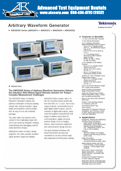
Arbitrary Waveform GeneratorAWG5000 Series (AWG5014 • AWG5012 • AWG5004 • AWG5002)The AWG5000 Series of Arbitrary Waveform Generators Delivers the Industry’s Best Mixed Signal Stimulus Solution for Today’s Complex Measurement ChallengesThe AWG5000 Series of Arbitrary Waveform Generators delivers theoptimal combination of industry leading sample rate, vertical resolution, signal fidelity and waveform memory length,all in an easy-to-use self-contained package.The series offers the industry’s best solution to the challenging signal stim-ulus issues faced by designers verifying,characterizing and debugging sophisti-cated electronic designs.Meeting the needs of today’s design engineers, the series provides excellent signal dynamic range and integrity.AWG5000 Series models, with a 14bits DA converter based sample rate from 600MS/s to 1.2GS/s, two to four output channels, synchronized four to eight digital marker outputs, and 28-channels of digital data outputs, easily solve the toughest measurement chal-lenges in wireless base band I/Q communications, digital consumer product design such as imaging devices, data conversion equipment and semiconductor design and test. The open Windows (Windows XP)-based instruments are easy and convenient to use and connect easily with peripherals and third-party software.AWG5000 Series.Features & Benefits1.2Gs/s and 600MS/s Models 14 bit Vertical Resolution 2 or 4Arbitrary WaveformDifferential/Single-ended Outputs –Up to 4.5V p-p Single-ended and 9V p-p at Differential Output into 50Ω–0.95ns Tr/Tf (10 to 90%) at 0.6V p-p–+/– 5ns Range (50ps Resolution) Inter Channel Skew Control–SFDR: 80dBc (1MHz),64dBc (10MHz)4 or 8Variable Level Marker Outputs–Up to 3.7V p-p Single-ended Output into 50Ω–300ps Tr/Tf (20 to 80%)at 0 to 1V–Up to 1ns Range (50ps Resolution) Delay Control28 Bits Ch 1/Ch 2Variable Level Digital Data Output–Up to 3.7V p-p Single-ended Output into 50Ω–300ps Tr/Tf (20 to 80%)at 0 to 1VUp to 32M Point Record Length For Longer Data Streams Down to 800ps Resolution Edge Timing Shift Control Real-time Sequencing Creates Infinite Waveform Loops, Jumps,and Conditional BranchesEasy to Use and Learn Shortens Test TimeIntuitive User Interface Based on Windows 2000 XP Convenient Bench Top Form FactorIntegrated PC Supports Network Integration and Provides a Built-in DVD, Removable Hard Drive,LAN and USB portsApplicationsDesigning, Testing and Deploying Wireless Communications: –High Fidelity QuadratureModulation I and Q Base-band Signals (Polar Modulation:I/Q + Magnitude Control, Two Pair of I/Q for MIMO)Imaging–Stimulus Signals for Imaging Display and Recording Devices (CCD, LCD)Data Conversion–Stimulus Signals for DataConversion Devices (ADC, DAC)Mixed Signal Design and Test –2/4Ch Analog + 4/8Ch Marker Outputs + 28 Bit Digital Data OutputsReal-world, Ideal or Distorted Signal Generation – Including All the Glitches, Anomalies and ImpairmentsEnhanced/Corrupted Playback of DSO Captured SignalsWaveform Vectors Imported from Third-party T ools such as MathCAD,MATLAB, Excel and OthersArbitrary Waveform GeneratorAWG5000 Series (AWG5014 • AWG5012 • AWG5004 • AWG5002)AWG5000 Series • /signal_sources2EVM/Constellation measurement.Typical Signal Injection.Arbitrary Waveform GeneratorAWG5000 Series (AWG5014 • AWG5012 • AWG5004 • AWG5002) RTSA Spectrum view.9-PAM with 250 Mbps.Mixed signal test by TDS/TLA iView.™AWG5000 Series • /signal_sources3Arbitrary Waveform GeneratorAWG5000 Series (AWG5014 • AWG5012 • AWG5004 • AWG5002)4AWG5000 Series • /signal_sourcesArbitrary Waveform GeneratorAWG5000 Series (AWG5014 • AWG5012 • AWG5004 • AWG5002)AWG5014AWG5012AWG5004AWG5002Arbitrary WaveformsWaveform Length 1 to 16,200,000 points (or 1 to 32,400,000 points,option 01)Number of Waveforms 1 to 16,000Sequence Length 1 to 4,000stepsSequence Repeat Counter 1 to 65,536 or infiniteSequence Control Repeat count,Trigger,Go-to-N and JumpJump Mode Synchronous and AsynchronousRun ModesContinuous Waveform is iteratively output.If a sequence is defined,the sequence order and repeat functions are appliedTriggered Waveform is output only once when an external,internal,GPIB,LAN or manual trigger is receivedGated Waveform begins output when gate is true and resets to beginning when falseSequence Waveform is output as defined by the sequenceClock GeneratorSampling Frequency10 MS/s to 1.2GS/s10 MS/s to 600 MS/sResolution8digitsInternal ClockAccuracy Within ±(1 ppm + Aging),Aging:within ±1 ppm/yearClock Phase Noise Less than –90dBc/Hz at 100kHz offsetInternal Trigger GeneratorInternal Trigger RateRange 1.0μs to 10.0sResolution3digits,0.1μs minimumSkew Control Between OutputsRange– 5 ns to + 5nsResolution5psAWG5000 Series • /signal_sources5Arbitrary Waveform GeneratorAWG5000 Series (AWG5014 • AWG5012 • AWG5004 • AWG5002)AWG5000 Series • /signal_sources6AWG5014AWG5012AWG5004AWG5002Main Arbitrary Waveform Output Resolution14 bitsAnalog OutputOutput StyleDifferential Output Impedance 50ΩConnectorBNC FrontAmplitude Output Voltage Normal:–4.5 V to + 4.5V,Direct –0.3V to +0.3V Amplitude Normal:20mV p-p to 4.5V p-p ,Direct; 20mV p-p to 0.6V p-pResolution 1mVDC Accuracy±(2.0% of Amplitude + 2mV) at offset = 0V Offset (into 50Ω) Range Normal:–2.25V to +2.25V,Direct:N/A Resolution 1mVAccuracy±(2% of offset +10mV at minimum amplitudePulse Response Rise/Fall time:(10% to 90%).Normal:1.4ns (2.0V p-p ),Direct:0.95ns (0.6V p-p )Bandwidth (–3dB)Normal:250MHz (2.0V p-p ),Direct:370MHz (0.6V p-p )Ringing Normal:750mV p-p (4.5V p-p filter through),80mV p-p (2.0V p-p filter through),Direct:60mV p-p (0.6V p-p )Low Pass Filter High range:100MHz,20MHz,Low range:through,100MHz,20MHz,Direct:N/ADelay from Marker Normal:17.5ns to 19.4ns (20MHz filter),3.8ns to 5.7ns (100MHz filter),0 to 1.9ns (Through),Direct:–1.5ns to 0.4nsSine Wave Characteristics (1.2GS/s clock,32 waveform points,37.5MHz signal frequency)(600MS/s clock,32 waveform points,18.75MHz signal frequency)Harmonics Normal:≤–40dBc (2.0V p-p ),Direct ≤=–49dBc (0.6V p-p )Normal:≤–46dBc (2.0V p-p ),Direct ≤=–55dBc (0.6V p-p )Non Harmonics Normal:≤–60dBc (2.0V p-p ,DC to 600MHz)Normal:≤–60dBc (2.0V p-p ,DC to 300MHz)Phase noise ≤–85dBc/Hz (2.0V p-p ,10kHz offset) –85dBc/Hz (2.0V p-p ,10kHz offset) SFDR 50dBc (Normal,37.5MHz,1.2GS/s,2.0V p-p )56dBc (Normal,18.75MHz,600MS/s,2.0V p-p )60dBc (Normal,10MHz,600MS/s,1.0V p-p )60dBc (Normal,10MHz,600MS/s,1.0V p-p )80dBc (Normal,1MHz,600MS/s,1.0V p-p )80dBc (Normal,1MHz,600MS/s,1.0V p-p )64dBc (Direct,10MHz,600 MS/s,0.6V p-p )64dBc (Direct,10MHz,600MS/s,0.6V p-p )80dBc (Direct,1MHz,600 MS/s,0.6V p-p )80dBc (Direct,1MHz,600MS/s,0.6V p-p )Arbitrary Waveform GeneratorAWG5000 Series (AWG5014 • AWG5012 • AWG5004 • AWG5002) Auxiliary OutputsOutput Style Single-endedOutput Impedance50ΩConnector BNC FrontLevel (into 50Ω)(Twice for Hi_Z input)Output Windows–1.00 V to + 2.7VAmplitude0.10 Vp-p to 3.7 Vp-pResolution10mVDC Accuracy±(10% of setting +120mV) Maximum Output Current±54mA /chRise/Fall Time (20% to 80%)300 ps(1.0 Vp-p,Hi +1.0V,Lo 0V) Skew Adjust Between MarkersRange0 to 1000ps Resolution50psRandom Jitter (Typical)1010 clock patternRMS5psrmsTotal Jitter (Typical)2^15–1PN data patternPeak to Peak (p-p)80psp-pClock (VCO) OutRange600MHz to 1.2GHzAmplitude0.4 Vp-pinto 50Ωto GND Impedance:50Ω,AC coupling Connector BNC Rear10MHz Reference OutAmplitude 1.2 Vp-p into 50Ω.Max 2.5 Vp-popenImpedance50Ω,AC couplingConnector BNC RearDC OutputsNumber of Outputs4:independently controlled outputsRange–3.0 to +5.0VResolution10mVMax.Current±100mAConnector2x4 pin header on front panelAWG5000 Series • /signal_sources7Arbitrary Waveform GeneratorAWG5000 Series (AWG5014 • AWG5012 • AWG5004 • AWG5002)AWG5000 Series • /signal_sources8Trigger In Impedance 1 k Ωor 50ΩPolarity POS or NEG ConnectorBNC FrontInput Voltage Range1 k Ω:±10V.50 Ω:±5V Threshold Level –5.0 V to 5.0VResolution 0.1VTrigger Jitter2.0ns to 4.5ns (Typical) Trigger Mode Minimum Pulse Width 20nsTrigger Hold-off 832* sampling_period – 100ns Delay to Analog Out128* sampling_period + 250ns Gate Mode Minimum Pulse Width 1024* sampling_period + 10ns Delay to Analog Out640* sampling_period + 260ns Event Input Impedance 1 k Ωor 50ΩPolarity POS or NEG ConnectorBNC FrontInput Voltage Range 1 k Ω:±10V.50 Ω:±5V Threshold –5.0 V to 5.0VResolution0.1VSequence Mode Mode Minimum Pulse Width 20nsEvent Hold Off 1024* Sampling Period + 10nsDelay to Analog Out640* Sampling Period + 280 ns (Jump timing:Asynchronous jump)External Clock IN Input Voltage Range 0.2 V p-p to 0.8 V p-p Impedance50Ω,AC coupledConnectorBNC RearReference Clock IN Input Voltage Range 0.2 V p-p to 3.0 V p-p Impedance50Ω,AC coupledFrequency Range 10MHz,20MHz,100MHz (with ±0.1%)ConnectorBNC RearPhase Lock IN Input Ranges5MHz to 600MHz (acceptable frequency drift is ±0.5%)Input Voltage Range 0.2 V p-p to 3 V p-pConnectorBNC RearAdd IN For each analog channel Impedance 50Ω,DC coupledDC Gain 1BandwidthDC to 100MHz at –3 dBInput Voltage Range ±1.0V ConnectorBNC RearArbitrary Waveform GeneratorAWG5000 Series (AWG5014 • AWG5012 • AWG5004 • AWG5002)(Third party software creation waveform data:MATLAB,MathCad,Excel)S/W driver for 3rd party S/W IVI-com driver and MATLAB libraryInstrument Control/Data Transfer PortsGPIB Remote control and data transfer.(Conforms to IEEE-Std 488.1,compatible with IEEE 488.2 and SCPI-1999.0)Ethernet (10/100/1000Base-T)Remote control and data transfer.(Conforms to IEEE 802.3).RJ-45Computer System & Peripherals Windows XP Professional,512 MB SDRAM,80 GB removable Hard Drive at rear (available front mount kit),CD-RW/DVD drive at front,included USB compact keyboard and mousePC I/O Ports USB 2.0 compliant ports (6 total,2 front,4 rear),PS/2mouse and keyboard connectors (rear panel),RJ-45 Ethernet connector (rear panel) supports 10/100/1000BASE-T,XGA outDisplay Characteristics10.4inch,LCD color display with touch screen,1024 (H)x768 (V) (XGA)Power Supply100 to 240VAC,47 to 63HzPower Consumption450WSafety UL61010-1,CAN/CSA-22.2,No.61010-1-04,EN61010-1,IEC61010-1Emissions EN 55011 (Class A),IEC61000-3-2,IEC61000-3-3Immunity IEC61326,IEC61000-4-2/3/4/5/6/8/11Regional CertificationsEurope EN61326Australia/New Zealand AS/NZS 2064AWG5000 Series • /signal_sources9Arbitrary Waveform GeneratorAWG5000 Series (AWG5014 • AWG5012 • AWG5004 • AWG5002)Ordering Information Arbitrary WaveformGenerator MainframeAWG50141.2GS/s,4-channel,14bits,16M point/channel Arbitrary Waveform Generator.AWG50121.2GS/s,2-channel,14bits,16M point/channel Arbitrary Waveform Generator.AWG5004600MS/s,4-channel,14bits,16M point/channel Arbitrary Waveform Generator.AWG5002600MS/s,2-channel,14bits,16M point/channel Arbitrary Waveform Generator.All Models Include:Accessory pouch,front cover, USB mouse,compact USB key board,lead set for DC output,stylus for touch screen 2 each, Windows®XP operating system restore DVD and instructions,AWG5000 Series product software CD and instructions,Document CD with Browser,Quick Start User Manual,registration card,Certificate of Calibration,power cable.Note:Please specify power cord and language option when ordering.Instrument OptionsAWG5014/AWG5012,AWG5004/AWG5002Opt.01 – Waveform Length Expansion (from 16 M to 32 M).AWG5012/AWG5002Opt. 03 –28 bits digital data outputs (digital data of ch 1 and ch 2).Common OptionsInternational Power PlugsOpt. A0 – North America power.Opt. A1 –Universal EURO power.Opt. A2 – United Kingdom power.Opt. A3 – Australia power.Opt. A5 – Switzerland power.Opt.A6 –Japan power.Opt.A10 – China power.Opt.A99 – No power cord or AC adapter.Language OptionsOpt. L0 – English.Opt. L5 – Japanese.Opt. L7 –Simplified Chinese.Opt. L8 – Traditional Chinese.ServiceOpt. CA1 – A single calibration event.Opt. C3 – Calibration service 3 years.Opt. C5 – Calibration service 5 years.Opt. D1 –Calibration data report.Opt. D3 – Calibration data report 3 years (withoption C3).Opt. D5 – Calibration data report 5 years (withoption C5).Opt. R3 –Repair service 3 years.Opt. R5 –Repair service 5 years.Post-sales Service Options:(e.g.,AWG5012-CA1).CA1 – A single calibration event.R3DW – Repair service coverage 3 years.R5DW – Repair service coverage 5 years.R2PW –Repair service coverage 2 yearspost warranty.R1PW –Repair service coverage 1 yearpost warranty.Product UpgradeAWG5014, AWG50UPOpt.M14 – Waveform Length Expansionfrom 16 M point to 32 M point.Product UpgradeAWG5012, AWG50UPOpt. M12 – Waveform Length Expansionfrom 16 M point to 32 M point.Opt.D13 –Digital Data Outputs.Product UpgradeAWG5004, AWG50UPOpt. M04 – Waveform Length Expansionfrom 16 M point to 32 M point.Product UpgradeAWG5002, AWG50UPOpt.M02 – Waveform Length Expansionfrom 16 M point to 32 M point.Opt.D03 –Digital Data Outputs.AWG5000 Series • /signal_sources 10Arbitrary Waveform GeneratorAWG5000 Series (AWG5014 • AWG5012 • AWG5004 • AWG5002)WarrantyOne-year parts and labor.AWG5000 Series • /signal_sources11Arbitrary Waveform GeneratorAWG5000 Series (AWG5014 • AWG5012 • AWG5004 • AWG5002)For Further InformationTektronix maintains a comprehensive, constantly expanding collection of application notes, technical briefs and other resources to help engineers working on the cutting edge of technology. Please visit Copyright © 2008, Tektronix. All rights reserved. Tektronix products are covered by U.S. and foreign patents, issued and pending. Information in this publication supersedes that in all previously published material.Specification and price change privileges reserved. TEKTRONIX and TEK are registered trademarks of Tektronix, Inc. All other trade names referenced are the service marks, trademarks or registered trademarks of their respective companies. 07/08 JS/WOW 76W-20381-3Contact Tektronix:ASEAN/Australasia (65) 6356 3900Austria +41 52 675 3777Balkans, Israel, South Africa and other ISE Countries +41 52 675 3777Belgium 07 81 60166Brazil & South America (11) 40669400Canada 1 (800) 661-5625Central East Europe, Ukraine and the Baltics +41 52 675 3777Central Europe & Greece +41 52 675 3777Denmark +45 80 88 1401Finland +41 52 675 3777France +33 (0) 1 69 86 81 81Germany +49 (221) 94 77 400Hong Kong (852) 2585-6688India (91) 80-22275577Italy +39 (02) 25086 1Japan 81 (3) 6714-3010Luxembourg +44 (0) 1344 392400Mexico, Central America & Caribbean 52 (55) 5424700Middle East, Asia and North Africa +41 52 675 3777The Netherlands ***********Norway 800 16098People’s Republic of China 86 (10) 6235 1230Poland +41 52 675 3777Portugal 80 08 12370Republic of Korea 82 (2) 6917-5000Russia & CIS +7 (495) 7484900South Africa +27 11 206 8360Spain (+34) 901 988 054Sweden 020 08 80371Switzerland +41 52 675 3777Taiwan 886 (2) 2722-9622United Kingdom & Eire +44 (0) 1344 392400USA 1 (800) 426-2200For other areas contact Tektronix, Inc. at: 1 (503) 627-7111Updated 12 November 2007roduct(s) are manufactured in ISO registered facilitie Product(s) complies with IEEE Standard 488.1-1987,RS-232-C,and with Tektronix Standard Codes and Formats.。
3GPP TS 36.213 V9.2.0 (2010-06)
3GPP TS 36.213 V9.2.0 (2010-06)Technical Specification3rd Generation Partnership Project;Technical Specification Group Radio Access Network; Evolved Universal Terrestrial Radio Access (E-UTRA);Physical layer procedures(Release 9)The present docu ment has been developed within the 3rd Generation Partnership Project (3G PP TM ) and may be fu rther elaborated for the purposes of 3GPP.The present d ocument has not been subject to any approval process by the 3G PP Organisational Partners and shall not be implemented.This Specification is provided for fu ture development work within 3GPP only. The Organisational Partners accept no liability for any use of this Specification. Specifications and reports for implementation of the 3GPP TM system should be obtained via the 3GPP Organisational Partners ‟ Publications Offices.KeywordsUMTS, radio, layer 13GPPPostal address3GPP support office address650 Route des Lucioles – Sophia AntipolisValbonne – FranceTel.: +33 4 92 94 42 00 Fax: +33 4 93 65 47 16InternetCopyright NotificationNo part may be reproduced except as authorized by written permission.The copyright and the foregoing restriction extend to reproduction in all media.© 2010, 3GPP Organizational Partners (ARIB, ATIS, CCSA, ETSI, TTA, TTC).All rights reserved.UMTS™ is a Trade Mark of ETSI registered for the benefit of its members3GPP™ is a Trade Mark of ETSI registered for the benefit of its Members and of the 3GPP Organizational PartnersLTE™ is a Trade Mark of ETSI currently being registered for the benefit of i ts Members and of the 3GPP Organizational Partners GSM® and the GS M logo are registered and owned by the GSM AssociationContentsForeword (5)1Scope (6)2References (6)3Definitions, symbols, and abbreviations (7)3.1Symbols (7)3.2Abbreviations (7)4Synchronisation procedures (8)4.1Cell search (8)4.2Timing synchroni sation (8)4.2.1Radio link monitoring (8)4.2.2Inter-cell synchronisation (8)4.2.3Transmission timing adjustments (8)5Power control (9)5.1Uplink power control (9)5.1.1Physical uplink shared channel (9)5.1.1.1UE behaviour (9)5.1.1.2Power headroom (12)5.1.2Physical uplink control channel (12)5.1.2.1UE behaviour (12)5.1.3Sounding Reference Symbol (14)5.1.3.1UE behaviour (14)5.2Downlink power allocation (15)5.2.1 eNodeB Relative Narrowband TX Power restrictions (16)6Random access procedure (16)6.1Physical non-synchronized random access procedure (17)6.1.1Timing (17)6.2Random Access Response Grant (17)7 Physical downlink shared channel related procedures (19)7.1UE procedure for receiving the physical downlink shared channel (19)7.1.1 Single-antenna port scheme (22)7.1.2Transmit diversity scheme (23)7.1.3Large delay CDD scheme (23)7.1.4Closed-loop spatial multiplexing scheme (23)7.1.5Multi-user MIMO scheme (23)7.1.5A Dual layer scheme (23)7.1.6Resource allocation (23)7.1.6.1Resource allocation type 0 (23)7.1.6.2Resource allocation type 1 (24)7.1.6.3Resource allocation type 2 (25)7.1.7Modulation order and transport block size determination (26)7.1.7.1Modulation order determination (27)7.1.7.2Transport block size determination (27)7.1.7.2.1Transport blocks not mapped to two-layer spatial multiplexing (28)7.1.7.2.2Transport blocks mapped to two-layer spatial multiplexing (34)7.1.7.2.3Transport blocks mapped for DCI Format 1C (34)7.1.7.3Redundancy Version determination for Format 1C (35)7.2UE procedure for reporting channel quality indication (CQI), precoding matrix indicator (PMI) and rankindication (RI) (35)7.2.1Aperiodic CQI/PMI/RI Reporting using PUSCH (38)7.2.2Periodic CQI/PMI/RI Reporting using PUCCH (42)7.2.3Channel quality indicator (CQI) definition (48)7.2.4Precoding Matrix Indicator (PMI) definition (50)7.3UE procedure for reporting ACK/NA CK (51)8Physical uplink shared channel related procedures (54)8.1Resource Allocation for PDCCH DCI Format 0 (57)8.2UE sounding procedure (57)8.3UE A CK/NACK procedure (60)8.4UE PUSCH Hopping procedure (60)8.4.1 Type 1 PUSCH Hopping (61)8.4.2 Type 2 PUSCH Hopping (62)8.5UE Reference Symbol procedure (62)8.6Modulation order, redundancy version and transport block size determination (62)8.6.1Modulation order and redundancy version determination (62)8.6.2Transport block size determination (64)8.6.3Control information MCS offset determination (64)8.7UE Transmit Antenna Selection (66)9Physical downlink control channel procedures (66)9.1UE procedure for determining physical downlink control channel assignment (66)9.1.1 PDCCH Assignment Procedure (66)9.1.2 PHICH Assignment Procedure (67)9.2PDCCH validation for semi-persistent scheduling (68)10Physical uplink control channel procedures (70)10.1UE procedure for determining physical uplink control channel assignment (70)10.2Uplink A CK/NACK timing (75)11 Physical multicast channel related procedures (76)11.1UE procedure for receiving the physical multicast channel (76)11.2UE procedure for receiving MCCH change notification (76)Annex A (informative): Change history (77)ForewordThis Technical Specification (TS) has been produced by the 3rd Generation Partnership Project (3GPP).The contents of the present document are subject to continuing work within the TSG and may change following formal TSG approval. Should the TSG modify the contents of this present document, it will be re-released by the TSG with an identifying change of release date and an increase in version number as follows:Version x.y.zwhere:x the first digit:1 presented to TSG for information;2 presented to TSG for approval;3 or greater indicates TSG approved document under change control.y the second digit is incremented for all changes of substance, i.e. technical enhancements, corrections, updates, etc.z the third digit is incremented when editorial only changes have been incorporated in the document.1 ScopeThe present document specifies and establishes the characteristics of the physicals layer procedures in the FDD and TDD modes of E-UTRA.2 ReferencesThe following documents contain provisions which, through reference in this text, constitute provisions of the present document.∙References are either specific (identified by date of publication, edition number, version number, etc.) or non-specific.∙For a specific reference, subsequent revisions do not apply.∙For a non-specific reference, the latest version applies. In the case of a reference to a 3GPP document (including a GSM document), a non-specific reference implicitly refers to the latest version of that document in the same Release as the present document.[1] 3GPP TR 21.905: “Vocabulary for 3GPP Specifications”[2] 3GPP TS 36.201: “Evolved Universal Terrestrial Radio Access (E-UTRA); Physical Layer –General Description”[3] 3GPP TS 36.211: “Evolved Universal Terrestrial Radio Access (E-UTRA); Physical channels andmodulation”[4] 3GPP TS 36.212: “Evolved Universal Terrestrial Radio Access (E-UTRA); Multiplexing andchannel c oding”[5] 3GPP TS 36.214: “Evolved Universal Terrestrial Radio Access (E-UTRA); Physical layer –Measurements”[6] 3GPP TS 36.101: “Evolved Universal Terrestrial Radio Access (E-UTRA); User Equipment (UE)radio transmission and reception”[7] 3GPP TS 36.104: “Evolved Universal Terrestrial Radio Access (E-UTRA); Base Station (BS)radio transmission and reception”[8] 3GPP TS36.321, “Evolved Universal Terrestrial Radio Access (E-UTRA); Medium AccessControl (MAC) protocol specification”[9] 3GPP TS36.423, “Evolved Universal Terrestrial Radio Access (E-UTRA); X2 ApplicationProtocol (X2AP)”[10] 3GPP TS36.133, “Evolved Universal Terrestrial Radio Access (E-UTRA); Requirements forsupport of radio resource management”[11] 3GPP TS36.331, “Evolved Universal Te rrestrial Radio Access (E-UTRA); Radio ResourceControl (RRC) protocol specification”3Definitions, symbols, and abbreviations3.1SymbolsFor the purposes of the present document, the following symbols apply:f nS ystem frame number as defined in [3]s nS lot number within a radio frame as defined in [3]DLRB N Downlink bandwidth configuration, expressed in units of RBsc N as defined in [3] UL RB NUplink bandwidth configuration, expressed in units of RB sc N as defined in [3]ULsymb N Number of SC-FDMA symbols in an uplink slot as defined in [3]RBsc NResource block size in the frequency domain, expressed as a number of subcarriers as defined in [3]s TBasic time unit as defined in [3]3.2 AbbreviationsFor the purposes of the present document, the following abbreviations apply. ACK Acknowledgement BCH Broadcast ChannelCCE Control Channel Element CQI Channel Quality Indicator CRC Cyclic Redundancy Check DAI Downlink Assignment Index DCI Downlink Control Information DLDownlinkDL-SCH Downlink Shared Channel DTX Discontinuous Transmission EPRE Energy Per Resource Element MCS Modulation and Coding Scheme NACK Negative Acknowledgement PBCH Physical Broadcast ChannelPCFICH Physical Control Format Indicator Channel PDCCH Physical Downlink Control Channel PDSCH Physical Downlink Shared ChannelPHICH Physical Hybrid ARQ Indicator Channel PMCH Physical Multicast ChannelPRA CH Physical Random Access Channel PRB Physical Resource BlockPUCCH Physical Uplink Control Channel PUSCH Physical Uplink Shared Channel QoS Quality of Service RBG Resource Block Group RE Resource Element RPF Repetition Factor RS Reference SignalSIR Signal-to-Interference RatioSINRSignal to Interference plus Noise Ratio SPS C-RNTI Semi-Persistent Scheduling C-RNTI SR Scheduling RequestSRS Sounding Reference Symbol TA Time alignmentTTI Transmission Time Interval UEUser EquipmentUL UplinkUL-SCH Uplink Shared ChannelVRB Virtual Resource Block4 Synchronisation procedures4.1 Cell searchCell search is the procedure by which a UE acquires time and frequency synchronization with a cell and detects the physical layer Cell ID of that cell. E-UTRA cell search supports a scalable overall transmission bandwidth corresponding to 6 resource blocks and upwards.The following signals are transmitted in the downlink to facilitate cell search: the primary and secondary synchronization signals.4.2 Timing synchronisation4.2.1 Radio link monitoringThe downlink radio link quality of the serving cell shall be monitored by the UE for the purpose of indicating out-of-sync/in-sync status to higher layers.In non-DRX mode operation, the physical layer in the UE shall every radio frame assess the radio link quality, evaluated over the previous time period defined in [10], against thresholds (Q out and Q in) defined by relevant tests in [10].In DRX mode operation, the physical layer in the UE shall at least once every DRX period assess the radio link quality, evaluated over the previous time period defined in [10], against thresholds (Q out and Q in) defined by relevant tests in [10].The physical layer in the UE shall in radio frames where the radio link quality is assessed indicate out-of-sync to higher layers when the radio link quality is worse than the threshold Q out. When the radio link quality is better than the threshold Q in, the physical layer in the UE shall in radio frames where the radio link quality is assessed indicate in-sync to higher layers.4.2.2 Inter-cell synchronisationNo functionality is specified in this section in this release.4.2.3 Transmission timing adjustmentsUpon reception of a timing advance command, the UE shall adjust its uplink transmission timing forPUCCH/PUSCH/SRS. The timing advance command indicates the change of the uplink timing relative to the current uplink timing as multiples of 16T. The start timing of the random access preamble is specified in [3].sIn case of random access response, 11-bit timing advance command [8], T A, indicates N TA values by index values ofT A = 0, 1, 2, ..., 1282, where an amount of the time alignment is given by N TA = T A⨯16. N TA is defined in [3].In other cases, 6-bit timing advance command [8], T A, indicates adjustment of the current N TA value, N TA,old, to the new N TA value, N TA,new, by index values of T A = 0, 1, 2,..., 63, where N TA,new = N TA,old + (T A-31)⨯16. Here, adjustment of N TA value by a positive or a negative amount indicates advancing or delaying the uplink transmission timing by a given amount respectively.For a timing advance command received on subframe n, the corresponding adjustment of the timing shall apply from the beginning of subframe n+6.When the UE‟s uplink PUCCH/PUSCH/SRS transmissions in subframe n and subframe n+1 are overlapped due to the timing adjustment, the UE shall transmit complete subframe n and not transmit the overlapped part of subframe n+1.If the received downlink timing changes and is not compensated or is only partly compensated by the uplink timing adjustment without timing advance command as specified in [10], the UE changes N TA accordingly.5 Power controlDownlink power control determines the energy per resource element (EPRE). The term resource element energydenotes the energy prior to CP insertion. The term resource element energy also denotes the average energy taken over all constellation points for the modulation scheme applied. Uplink power control determines the average power over a SC-FDMA symbol in which the physical channel is transmitted.5.1 Uplink power controlUplink power control controls the transmit power of the different uplink physical channels.A cell wide overload indicator (OI) and a High Interference Indicator (HII) to control UL interference are defined in [9].5.1.1Physical uplink shared channel5.1.1.1UE behaviourThe setting of the UE Transmit power PUSCH P for the physical uplink shared channel (PUSCH) trans mission in subframe i is defined by)}()()()())((log10,min{)(TF O_PUSCH PUSCH10CMAX PUSCH i f i PL j j P i MP i P +∆+⋅++=α [dBm]where,∙ CMAX P is the configured UE transmitted power defined in [6]∙ )(PUSCH i M is the bandwidth of the PUSCH resource assignment expressed in number of resource blocks validfor subframe i .∙)(O_PUSCH j P is a parameter composed of the sum of a cell specific nominal component )( PUSCHO_NOMINAL_j Pprovided from higher layers for j=0 and 1 and a UE specific component )(O_UE_PUSCH j P provided by higher layers for j=0 and 1. For PUSCH (re)transmissions corresponding to a semi-persistent grant then j=0 , for PUSCH (re)transmissions corresponding to a dynamic scheduled grant then j=1 and for PUSCH(re)trans missions corresponding to the random access response grant then j=2. 0)2(O_UE_PUSCH =P and 3_O_PRE PUSCHO_NOMINAL_)2(Msg PREAMBLEP P ∆+=, where the parameterPREAMBLE_INITIA L_RECEIVED_TA RGET_POW ER [8] (O_PRE P ) and 3_Msg PREAMBLE ∆ are signalledfrom higher layers. ∙For j =0 or 1, {}1,9.0,8.0,7.0,6.0,5.0,4.0,0∈α is a 3-bit cell specific parameter provided by higher layers. For j=2, .1)(=j α∙PL is the downlink pathloss estimate calculated in the UE in dB and PL = referenceSignalPower – higher layer filtered RSRP, where referenceSignalPower is provided by higher layers and RSRP is defined in [5] and the higher layer filter configuration is defined in [11]∙T F 10()10log ((21))SM PR K PUSC Hoffseti β⋅∆=-for 25.1=S K and 0 for 0=S K where S K is given by the UE specificparameter deltaMCS-Enabled provided by higher layerso/CQIRE MPR O N =for control data sent via PUSCH without UL-SCH data and1/C rRE r KN -=∑for othercases.▪where C is the number of code blocks, r K is the size for code block r , CQI O is the number of CQI bits including CRC bits and RE N is the number of resource elementsdetermined as initial-PUSCH symbN M N initialPUSCHscRE ⋅=-, where C , r K , initialPUSCH scM- andinitial-PUSCH symbN are defined in [4].oPUSCHCQIoffsetoffset ββ= for control data sent via PUSCH without UL-SCH data and 1 for other cases.∙PUSCH δ is a UE specific correction value, also referred to as a TPC command and is included in PDCCH withDCI format 0 or jointly coded with other TPC commands in PDCCH with DCI format 3/3A whose CRC parity bits are scrambled with TPC-PUSCH-RNTI. The current PUSCH power control adjustment state is given by )(i f which is defined by:o)()1()(PUSCH PUSCH K i i f i f -+-=δ if accumulation is enabled based on the UE-specific parameterAccumulation-enabled provided by higher layers or if the TPC command PUSCH δ is included in a PDCCH with DCI format 0 where the CRC is scrambled by the Temporary C-RNTI▪where )(PUSCH PUSCH K i -δwas signalled on PDCCH with DCI format 0 or 3/3A on subframe PUSCH K i -, and where )0(f is the first value after reset of accumulation. ▪The value of PUSCH K is∙ For FDD,PUSCH K = 4∙ For TDD UL/DL configurations 1-6, PU SC H K is given in Table 5.1.1.1-1∙For TDD UL/DL configuration 0o If the PUSCH transmission in subframe 2 or 7 is scheduled with a PDCCHof DCI format 0 in which the LSB of the UL index is set to 1, PUSC H K = 7 o For all other PUSCH transmissions,PU SC HK is given in Table 5.1.1.1-1.▪The UE attempts to decode a PDCCH of DCI format 0 with the UE ‟s C-RNTI or SPS C-RNTI and a PDCCH of DCI format 3/3A with this UE ‟s TPC-PUSCH-RNTI in every subframe except when in DRX▪If DCI format 0 and DCI format 3/3A are both detected in the same s ubframe, then the UE shall use the PUSCH δ provided in DCI format 0.▪ 0PUSCH =δdB for a subframe where no TPC command is decoded or where DRX occurs ori is not an uplink subframe in TDD.▪The PUSCH δ dB accumulated values signalled on PDCCH with DCI format 0 are given in Table 5.1.1.1-2. If the PDCCH with DCI format 0 is validated as a SPS activation or release PDCCH, then PUSCH δ is 0dB.▪The PUSCH δ dB accumulated values signalled on PDCCH with DCI format 3/3A are one of SET1 given in Table 5.1.1.1-2 or SET2 given in Table 5.1.1.1-3 as determined by the parameter TPC-Index provided by higher layers.▪ If UE has reached maximum power, positive TPC commands shall not be accumulated ▪ If UE has reached minimum power, negative TPC commands shall not be accumulated ▪UE shall reset accumulation∙when O_UE_PUSCHP value is changed by higher layers∙when the UE receives random access response messageo)()(PUS CH PUS CH K i i f -=δif accumulation is not enabled based on the UE-specific parameterAccumulation-enabled provided by higher layers▪where )(PUSCH PUSCH K i -δwas signalled on PDCCH with DCI format 0 on subframePUSCH K i -▪The value of PUSCH K is∙ For FDD,PUSCH K = 4∙ For TDD UL/DL configurations 1-6, PU SC H K is given in Table 5.1.1.1-1∙For TDD UL/DL configuration 0o If the PUSCH transmission in subframe 2 or 7 is scheduled with aPDCCHof DCI format 0 in which the LSB of the UL index is set to 1, PUSC H K = 7 o For all other PUSCH transmissions, PU SC H Kis given in Table 5.1.1.1-1.▪The PUSCH δ dB absolute values signalled on PDCCH with DCI format 0 are given in Table 5.1.1.1-2. If the PDCCH with DCI format 0 is validated as a SPS activation or release PDCCH, then PUSCH δ is 0dB.▪)1()(-=i f i f for a subframe where no PDCCH with DCI format 0 is decoded or whereDRX occurs or i is not an uplink subframe in TDD.o For both types of )(*f (accumulation or current absolute) the first value is set as follows:▪If O_UE_PUS C HP value is changed by higher layers, ∙()00f =▪Else∙2)0(msg rampup P f δ+∆=o where 2msg δ is the TPC command indicated in the random accessresponse, see Section 6.2, and orampup P ∆ is provided by higher layers and corresponds to the total powerramp-up from the first to the last preambleTable 5.1.1.1-1PU SC HK for TDD configuration 0-6Table 5.1.1.1-2: Mapping of TPC Command Field in DCI format 0/3 to absolute and accumulatedPUSCH δ values.Table 5.1.1.1-3: Mapping of TPC Command Field in DCI format 3A to accumulated PUSCH δ values.5.1.1.2 Power headroomThe UE power headroom PH valid for subframe i is defined by{}CM AX 10PUSCH O_PUSCH TF ()10log (())()()()()PH i P M i P j j PL i f i α=-++⋅+∆+ [dB]where, CMAX P , )(PUS C H i M , )(O_PUS C H j P , )(j α, PL, )(TF i ∆ and )(i f are defined in section 5.1.1.1. The power headroom shall be rounded to the closest value in the range [40; -23] dB with steps of 1 dB and is delivered by the physical layer to higher layers.5.1.2Physical uplink control channel5.1.2.1UE behaviourThe setting of the UE Transmit power PUCCH P for the physical uplink control channel (PUCCH) transmission in subframe i is defined by()()()(){}i g F n n h PL P P i P HARQCQI +∆+++=F_PUCCH0_PUCCH CMAX PUCCH ,,min [dBm]where∙ CMAX P is the configured UE transmitted power defined in [6]∙The parameter F_PUCCH ()F ∆ is provided by higher layers. Each F_PUCCH ()F ∆ value corresponds to a PUCCH format (F ) relative to PUCCH format 1a, where each PUCCH format (F ) is defined in Table 5.4-1 [3].∙(),CQI HARQ h n n is a PUCCH format dependent value, where CQI n corresponds to the number of informationbits for the channel quality information defined in section 5.2.3.3 in [4] and HARQ n is the number of HA RQ bits.o For PUCCH format 1,1a and 1b ()0,=HARQ CQI n n h o For PUCCH format 2, 2a, 2b and normal cyclic prefix()⎪⎩⎪⎨⎧≥⎪⎪⎭⎫ ⎝⎛=otherwise04if 4log 10,10CQI CQI HARQCQI n n n n ho For PUCCH format 2 and extended cyclic prefix()1010log if 4,40otherw iseC Q I H ARQ C Q I H ARQ C Q I H ARQn n n n h n n ⎧+⎛⎫+≥⎪ ⎪ ⎪=⎨⎝⎭⎪⎩∙O_PUCCH P is a parameter composed of the sum of a cell specific parameter PUCCHO_NOMINAL_P provided byhigher layers and a UE specific component O_UE_PUCCHP provided by higher layers.∙PUCCH δ is a UE specific correction value, also referred to as a TPC command, included in a PDCCH with DCIformat 1A/1B/1D/1/2A/2/2B or sent jointly coded with other UE specific PUCCH correction values on a PDCCH with DCI format 3/3A whose CRC parity bits are scrambled with TPC-PUCCH-RNTI.o The UE attempts to decode a PDCCH of DCI format 3/3A with the UE ‟s TPC-PUCCH-RNTI and oneor several PDCCHs of DCI format 1A/1B/1D/1/2A/2/2B with the UE ‟s C-RNTI or SPS C-RNTI on every subframe except when in DRX. o If the UE decodes a PDCCH with DCI format 1A/1B/1D/1/2A/2/2B and the corresponding detectedRNTI equals the C-RNTI or SPS C-RNTI of the UE, the UE shall use the PUCCH δ provided in that PDCCH.else▪if the UE decodes a PDCCH with DCI format 3/3A, the UE shall use the PUCCH δ provided in that PDCCHelse the UE shall set PUCCH δ = 0 dB.o 1()(1)()M PU C C H m m g i g i i k δ-==-+-∑where )(i g is the current PUCCH power control adjustmentstate and where ()0g is the first value after reset.▪ For FDD, 1=M and 40=k .▪ For TDD, values of M and m k are given in Table 10.1-1.▪The PUCCH δ dB values signalled on PDCCH with DCI format 1A/1B/1D/1/2A/2/2B are given in Table 5.1.2.1-1. If the PDCCH with DCI format 1/1A/2/2A/2B is validated as an SPS activation PDCCH, or the PDCCH with DCI format 1A is validated as an SPS release PDCCH, then PUCCH δ is 0dB. ▪ The PUCCH δ dB values signalled on PDCCH with DCI format 3/3A are given in Table 5.1.2.1-1 or in Table 5.1.2.1-2 as semi-statically configured by higher layers. ▪If O_UE_PUC C HP value is changed by higher layers,∙()00g =▪Else∙2(0)rampup msg g P δ=∆+o where 2msg δ is the TPC command indicated in the random accessresponse, see Section 6.2 and orampup P ∆ is the total power ramp -up from the first to the last preambleprovided by higher layers▪ If UE has reached maximum power, positive TPC commands shall not be accumulated ▪ If UE has reached minimum power, negative TPC commands shall not be accumulated ▪UE shall reset accumulation∙ when O_UE_PUCCHP value is changed by higher layers∙when the UE receives a random access response message▪()(1)g i g i =- if i is not an uplink subframe in TDD.Table 5.1.2.1-1: Mapping of TPC Command Field in DCI format 1A/1B/1D/1/2A/2B/2/3 to PUCCH δvalues.Table 5.1.2.1-2: Mapping of TPC Command Field in DCI format 3A to PUCCH δ values.5.1.3Sounding Reference Symbol5.1.3.1UE behaviourThe setting of the UE Transmit power SRS P for the Sounding Reference Symbol transmitted on subframe i is defined bySRS CM AX SRS_OFFSET 10SRS O_PUSCH ()min{,10log ()()()()}P i P P M P j j PL f i α=+++⋅+ [dBm]where∙ CMAX P is the configured UE transmitted power defined in [6]∙For 1.25S K =,SRS_OFFSET P is a 4-bit UE specific parameter semi-statically configured by higher layers with1dB step size in the range [-3, 12] dB. ∙For 0=S K ,SRS_OFFSETP is a 4-bit UE specific parameter semi-statically configured by higher layers with 1.5dB step size in the range [-10.5,12] dB ∙SRS M is the bandwidth of the SRS transmission in subframe i expressed in number of resource blocks.∙ )(i f is the current power control adjustment state for the PUSCH, see Section 5.1.1.1.∙ )(O_PUSCH j P and )(j α are parameters as defined in Section 5.1.1.1, where 1=j .5.2 Downlink power allocationThe eNodeB determines the downlink trans mit energy per resource element.A UE may assume downlink cell-specific RS EPRE is constant across the downlink system bandwidth and constant across all subframes until different cell-specific RS power information is received. The downlink reference-signal EPRE can be derived from the downlink reference-signal transmit power given by the parameter Reference-signal-power provided by higher layers. The downlink reference-signal transmit power is defined as the linear average over the power contributions (in [W]) of all resource elements that carry cell-specific reference signals within the operating system bandwidth.The ratio of PDSCH EPRE to cell-specific RS EPRE among PDSCH REs (not applicable to PDSCH REs with zero EPRE) for each OFDM symbol is denoted by either A ρ or B ρaccording to the OFDM symbol index as given by Table 5.2-2. In addition,A ρ and B ρare UE-specific.For a UE in transmission mode 8 when UE-specific RSs are not present in the PRBs upon which the correspondingPDSCH is mapped or in trans mission modes 1 – 7, the UE may assume that for 16 QAM, 64 QAM, spatial multiplexing with more than one layer or for PDSCH transmissions associated with the multi-user MIMO transmission scheme,▪A ρ is equal to )2(log1010offset-power++A P δ [dB] when the UE receives a PDSCH data transmission usingprecoding for transmit diversity with 4 cell-specific antenna ports according to Section 6.3.4.3 of [3]; ▪A ρ is equal to A P +offset-powerδ [dB] otherwisewhere offset-power δis 0 dB for all PDSCH transmission schemes except multi-user MIMO and where A P is a UE specificparameter provided by higher layers.For transmission mode 7, if UE-specific RSs are present in the PRBs upon which the corresponding PDSCH is mapped, the ratio of PDSCH EPRE to UE-specific RS EPRE within each OFDM symbol containing UE-specific RSs shall be a constant, and that constant shall be maintained over all the OFDM symbols containing the UE-specific RSs in the corresponding PRBs. In addition, the UE may assume that for 16QAM or 64QAM, this ratio is 0 dB.For transmission mode 8, if UE-specific RSs are present in the PRBs upon which the corresponding PDSCH is mapped, the UE may assume the ratio of PDSCH EPRE to UE-specific RS EPRE within each OFDM symbol containing UE-specific RSs is 0 dB.A UE may assume that downlink positioning reference signal EPRE is constant across the positioning reference signal bandwidth and across all OFDM symbols that contain positioning reference signals in a given positioning reference signal occasion [10].The cell-specific ratio A B ρρ/ is given by Table 5.2-1 according to cell-specific parameter B P signalled by higher layers and the number of configured eNodeB cell specific antenna ports.Table 5.2-1: The cell-specific ratio A B ρρ/ for 1, 2, or 4 cell specific antenna ports。
OXuPCI954_DS

External—Free ReleaseOxford Semiconductor, Inc.1900 McCarthy Boulevard, Suite 210 © Oxford Semiconductor, Inc. 2007F EATURES• Four 16C950 High performance UART channels • 8-bit Pass-through Local Bus (PCI Bridge )• IEEE1284 Compliant SPP/EPP/ECP parallel port (with external transceiver)• Efficient 32-bit, 33 MHz, multi-function target-only PCIcontroller, fully compliant to PCI Local Bus Specification 3.0 and PCI Power Management Specification 1.1 • Software compatible with OXmPCI954• UARTs fully software compatible with 16C550-type devices • UART operation up to 60 MHz via external clock source. Up to 20 MHz with the crystal oscillator• Baud rates up to 60 Mbps in external 1x clock mode and 15 Mbps in asynchronous mode• 128-byte deep FIFO per transmitter and receiver • Flexible clock prescaler, from 1 to 31.875• Automated in-band flow control using programmable Xon/Xoff in both directions•Automated out-of-band flow control using CTS#/RTS# and/or DSR#/DTR#• Programmable RS485 turnaround delay• Arbitrary trigger levels for receiver and transmitter FIFO interrupts and automatic in-band and out-of-band flow control• Infra-red (IrDA) receiver and transmitter operation • 9-bit data framing, as well as 5, 6, 7, and 8 bits • Detection of bad data in the receiver FIFO• Global Interrupt Status and readable FIFO levels to facilitate implementation of efficient device drivers.• Local registers to provide status/control of device functions • 11 multi-purpose I/O pins, which can be configured as input interrupt pins or ‘wake-up’• Auto-detection of a wide range of optional MICROWIRE TM compatible EEPROMs, to re-configure device parameters • Function access , to pre-configure each function prior to handover to generic device drivers • Operation via I/O or memory mapping• 3.3 V or 5 V operation (PCI Universal Voltage)• Extended operating temperature range: -40° C to 85° C •176-pin LQFP packageD ESCRIPTIONThe OXuPCI954 is a single chip solution for PCI-based serial and parallel expansion add-in cards. It is a dual function PCI device, where function 0 offers four ultra-high performance OX16C950 UARTs, and function 1 is configurable either as an 8-bit local bus or a bi-directional parallel port.Each UART channel in the OXuPCI954 is the fastest available PC-compatible UART, offering data rates up to 15 Mbps and 128-byte deep transmitter and receiver FIFOs. The deep FIFOs reduce CPU overhead and allow utilization of higher data rates. Each UART channel is software compatible with the widely used industry-standard 16C550 devices (and compatibles), as well as the OX16C95x family of high performance UARTs. In addition to increased performance and FIFO size, the UARTs also provide the full set of OX16C95x enhanced features including automated in-band flow control, readable FIFO levels, etc.To enhance device driver efficiency and reduce interrupt latency, internal UARTs have multi-port features such as shadowed FIFO fill levels, a global interrupt source register and Good-Data Status, readable in four adjacent DWORD registers visible to logical functions in I/O space and memory space.Expansion of serial ports beyond four channels is possible using the 8-bit pass-through Local Bus function. This provides a general address/data bus and interrupt capability to a discrete UART part, such as the Oxford SemiconductorOX16C954. Other controllers could be used to provide capabilities beyond additional UART ports. The addressable space provided by the Local Bus can be increased up to 256 bytes, and divided into four chip-select regions. This flexible expansion scheme caters for cards with up to 20 serial ports using external 16C950, 16C954 or compatible devices, or composite applications such as combined serial and parallel port expansion cards. Serial port cards with up to 20 ports (or with 4 serial ports and a parallel port) can be designed without redefining any device or timing parameters.The parallel port is an IEEE 1284 compliant SPP/EPP/ECP parallel port that fully supports the existing Centronics interface. The parallel port can be enabled in place of the local bus. A n external bus transceiver is required for 5V parallel port operation if device is 3.3V sourced.For full flexibility, all the default configuration register values can be overwritten using an optional M ICROWIRE compatibleserial EEPROM. This EEPROM can also be used to provide function access to pre-configure devices on the local bus/parallel port, prior to any PCI configuration accesses and before control is handed to (generic) device drivers.The OXuPCI954 can be used to replace the OXmPCI954 in a PCI application where quad UARTs and a local bus/parallel port functionality are required.OXuPCI954 DATA SHEETIntegrated High Performance Quad UARTs,8-bit Local Bus/Parallel Port,3.3 V and 5 V (Universal Voltage) PCI Interface .Improvements of the OXuPCI954 over Discrete SolutionsHigher degree of integrationThe OXuPCI954 device offers four internal 16C950 high-performance UARTs and an 8-bit local bus or abi-directional parallel port.Multi-function deviceThe OXuPCI954 is a multi-function device to enable users to load individual device drivers for the internal serial ports, drivers for the peripheral devices connected to the local bus or drivers for the internal parallel port.Quad Internal OX16C950 UARTsThe OXuPCI954 device contains four ultra-high performance UARTs, which can increase driver efficiency by using features such as the 128-byte deep transmitter and receiver FIFOs, flexible clock options, automatic flow control, programmable interrupt and flow control trigger levels and readable FIFO levels. Data rates are up to 60 Mbps.Improved access timingAccess to the internal UARTs require zero or one PCI wait state. A PCI read transaction from an internal UART can complete within five PCI clock cycles and a write transaction to an internal UART can complete within four PCI clock cycles. Reduces interrupt latencyThe OXuPCI954 device offers shadowed FIFO levels and Interrupt status registers on the internal UARTs and the MIO pins. This reduces the device driver interrupt latency. Power managementThe OXuPCI954 device complies with the PCI Power Management Specification 1.1 and the Microsoft Communications Device-class Power Management Specification 2.0 (2000). Both functions offer the extended capabilities for Power Management. This achieves significant power savings by enabling device drivers to power down the PCI functions. For function 0, this is through switching off the channel clock, in power state D3. Wake-up (PME# generation) can be requested by either functions. For function 0, this is via the RI# inputs of the UARTs in the power-state D3 or any modem line and SIN inputs of the UARTs in power-state D2. For function 1, this is via the MIO[2] input.Optional EEPROMThe OXuPCI954 device can be reconfigured from an external EEPROM to the end-user’s requirements. However, this is not required in many applications as the default values are sufficient for typical applications. An overrun detection mechanism built into the EEPROM controller prevents the PCI system from ‘hanging’ due to an incorrectly programmed EEPROM.R EVISION H ISTORYRevision Modification May 2007 First publication.Sep 2007 Feature revision, including removal of D3coldT ABLE OF C ONTENTS1OXuPCI954 Device Modes (6)2Block Diagram (7)3Pin Information—176-Pin LQFP (8)3.1Mode ‘0’ Quad UARTs + 8-bit Local Bus (8)3.1.1Mode ‘1’ : Quad UARTs + Parallel Port (9)3.2Pin Descriptions (10)4Configuration and Operation (16)5PCI Target Controller (17)5.1Operation (17)5.2Configuration Space (17)5.2.1PCI Configuration Space Register Map (18)5.3Accessing Logical Functions (20)5.3.1PCI Access to Internal UARTs (21)5.3.2PCI Access to 8-bit Local Bus (22)5.3.3PCI Access to Parallel Port (22)5.4Accessing Local Configuration Registers (23)5.4.1Local Configuration and Control Register ‘LCC’ (Offset 0x00) (23)5.4.2Multi-purpose I/O Configuration Register ‘MIC’ (Offset 0x04) (24)5.4.3Local Bus Timing Parameter Register 1 ‘LT1’ (Offset 0x08) (26)5.4.4Local Bus Timing Parameter Register 2 ‘LT2’ (Offset 0x0C) (27)5.4.5UART Receiver FIFO Levels ‘URL’ (Offset 0x10) (28)5.4.6UART Transmitter FIFO Levels ‘UTL’ (Offset 0x14) (29)5.4.7UART Interrupt Source Register ‘UIS’ (Offset 0x18) (29)5.4.8Global Interrupt Status and Control Register ‘GIS’ (Offset 0x1C) (30)5.5PCI Interrupts (31)5.6Power Management (32)5.6.1Power Management of Function 0 (32)5.6.2Power Management of Function 1 (33)5.6.3Universal Voltage (34)5.7Unique Bar Option – for Function 0 (35)6Internal OX16C950 UARTs (36)6.1Operation – Mode Selection (36)6.1.1450 Mode (36)6.1.2550 Mode (36)6.1.3Extended 550 Mode (36)6.1.4750 Mode (36)6.1.5650 Mode (36)6.1.6950 Mode (37)6.2Register Description Tables (38)6.3UART Reset Configuration (41)6.3.1Hardware Reset (41)6.3.2Software Reset (41)6.4Transmitter and Receiver FIFOs (42)6.4.1FIFO Control Register ‘FCR’ (42)6.5Line Control and Status (43)6.5.1False Start Bit Detection (43)6.5.2Line Control Register ‘LCR’ (43)6.5.3Line Status Register ‘LSR’ (44)6.6Interrupts and Sleep Mode (45)6.6.1Interrupt Enable Register ‘IER’ (45)6.6.2Interrupt Status Register ‘ISR’ (46)6.6.3Interrupt Description (46)6.6.4Sleep Mode (47)6.7Modem Interface (47)6.7.1Modem Control Register ‘MCR’ (47)6.7.2Modem Status Register ‘MSR’ (48)6.8Other Standard Registers (48)6.8.1Divisor Latch Registers ‘DLL and DLM’ (48)6.8.2Scratch Pad Register ‘SPR’ (48)6.9Automatic Flow Control (49)6.9.1Enhanced Features Register ‘EFR’ (49)6.9.2Special Character Detection (50)6.9.3Automatic In-band Flow Control (50)6.9.4Automatic Out-of-band Flow Control (50)6.10Baud Rate Generation (51)6.10.1General Operation (51)6.10.2Clock Prescaler Register ‘CPR’ (51)6.10.3Times Clock Register ‘TCR’ (51)6.10.4External 1x Clock Mode (53)6.10.5Crystal Oscillator Circuit (53)6.11Additional Features (54)6.11.1Additional Status Register ‘ASR’ (54)6.11.2FIFO Fill Levels ‘TFL and RFL’ (54)6.11.3Additional Control Register ‘ACR’ (54)6.11.4Transmitter Trigger Level ‘TTL’ (55)6.11.5Receiver Interrupt. Trigger Level ‘RTL’ (55)6.11.6Flow Control Levels ‘FCL’ and ‘FCH’ (56)6.11.7Device Identification Registers (56)6.11.8Clock Select Register ‘CKS’ (56)6.11.9Nine-bit Mode Register ‘NMR’ (57)6.11.10Modem Disable Mask ‘MDM’ (57)6.11.11Readable FCR ‘RFC’ (58)6.11.12Good-data Status Register ‘GDS’ (58)6.11.13Port Index Register ‘PIX’ (58)6.11.14Clock Alteration Register ‘CKA’ (58)6.11.15RS485 Delay Enable ‘RS485_DLYEN’ (58)6.11.16RS485 Delay Count ‘RS485_DLYCNT’ (59)7Local bus (60)7.1Overview (60)7.2Operation (60)7.3Configuration and Programming (61)8Bidirectional Parallel Port (62)8.1Operation and Mode Selection (62)8.1.1SPP Mode (62)8.1.2PS2 Mode (62)8.1.3EPP Mode (62)8.1.4ECP Mode (62)8.2Parallel Port Interrupt (63)8.3Register Description (63)8.3.1Parallel Port Data Register ‘PDR’ (64)8.3.2ECP FIFO Address / RLE (64)8.3.3Device Status Register ‘DSR’ (64)8.3.4Device Control Register ‘DCR’ (64)8.3.5EPP Address register ‘EPPA’ (65)8.3.6EPP Data Registers ‘EPPD1-4’ (65)8.3.7ECP Data FIFO (65)8.3.8Test FIFO (65)8.3.9Configuration A Register (65)8.3.10Configuration B Register (65)8.3.11Extended Control Register ‘ECR’ (65)9Serial EEPROM (66)9.1Specification (66)9.1.1Zone 0: Header (67)9.1.2Zone 1: Local Configuration Registers (68)9.1.3Zone 2: Identification Registers (69)9.1.4Zone 3: PCI Configuration Registers (69)9.1.5Zone 4: Power Management DATA (and DATA_SCALE Zone) (70)9.1.6Zone 5: Function Access (70)10Operating Conditions (72)10.1DC Electrical Characteristics (72)11AC Electrical Characteristics (76)11.1PCI Bus Timings (76)11.2Local Bus (77)11.3Serial Ports (79)12Timing Waveforms (80)13Package Information (95)13.1176-Pin LQFP (95)14Ordering Information (96)1OX U PCI954D EVICE M ODESThe OXuPCI954 supports two modes of operation. These modes are summarized in the following table.Device Mode Mode Pin Selection Functionality0 MODE = 0 Function 0 : Quad UARTs Function 1 : 8-bit local bus1 MODE = 1 Function 0 : Quad UARTs Function 1 : Parallel Port* The OXuPCI954 is not pin-compatible with the OX16PCI954 or the OXmPCI954, but is the same in all other aspects.2B LOCK D IAGRAMFIFOSELMODEAD[31:0]C/BE[3:0]#PCI_CLKFRAME#DEVSEL#IRDY#TRDY#STOP#PARPERR#IDSELRST#INTA#PME#XTLIXTLOUART_Clk_Out Local_Bus ClkEE_DIEE_CSEE_CKEE_DOSOUT[3:0]SIN[3:0]RTS[3:0]DTR[3:0]CTS[3:0]DSR[3:0]DCD[3:0]RI[3:0]MIO[10:0]PD[7:0]ACK#PEBUSYSLCTERR#SLIN#INIT#AFD#STB#LBA[7:0]LBD[7:0]LBCS[3:0]LBWR#LBRD#LBRSTDATA_DIR OXuPCI954 Block DiagramOSCDIS XTLSEL3P IN I NFORMATION—176-P IN LQFP 3.1Mode ‘0’ Quad UARTs + 8-bit Local Bus7 NC. Do not connect these pins:23, 40, 41, 136, 137, 138, 1393.1.1Mode ‘1’ : Quad UARTs + Parallel Port15 NC. Do not connect these pins:23, 40, 41, 74, 112, 113, 114, 115, 116, 117, 124, 136, 137, 138, 1393.2Pin DescriptionsFor the actual pinouts of the OXuPCI954 device (for the various modes), refer to the Section 3, Pin Information. The I/O direction key table is on page 15.PCI Interface – All ModesPin Dir1Name Description149, 150, 151, 154, 155,157, 158, 160, 164, 165,167, 168, 169, 170, 171,174, 13, 14, 15, 17, 18, 20,24, 25, 27, 28, 31, 32, 33,34, 35, 39P_I/O AD[31:0] Multiplexed PCI Address/Data bus161, 175, 12, 26 P_I C/BE[3:0]# PCI Command/Byte enable146 P_I CLK PCI system clock (33MHz)176 P_IFRAME#CycleFrame5 P_ODEVSEL#DeviceSelect1 P_IIRDY#Initiatorready2 P_OTRDY#Targetready6 P_O STOP# Target Stop request10 P_I/OPAR Parity8 P_OSERR#Systemerror7 P_I/OPERR#Parityerror163 P_I IDSEL Initialization device select144 P_I RST# PCI system reset142 P_ODINTA# PCIinterrupt147 P_OD PME# Power management eventSerial Port Pins – All ModesPin Dir1Name Description50 I FIFOSEL FIFO select. For backward compatibility with 16C550,16C650 and 16C750 devices the UARTs’ FIFO depth is 16when FIFOSEL is low. The FIFO size is increased to 128when FIFOSEL is high. The unlatched state of this pin isreadable by software. The FIFO size may also be set to 128by setting FCR[5] when LCR[7] is set, or by putting thedevice into Enhanced mode.82, 81, 63, 62 O(h)SOUT[3:0]IrDA_Out[3:0] These four pins are present in all modes but they can serve one of two functions, as follows:UART serial data outputs.UART IrDA data output when MCR[6] of the corresponding channel is set in Enhanced mode.91, 73, 72, 55I(h) I(h) SIN[3:0]IrDA_In[3:0]These four pins are present in all modes but they can serveone of two functions, as follows:UART serial data inputs.UART IrDA data input when IrDA mode is enabled (seeabove).Serial Port Pins – All ModesPin Dir1Name Description89, 76, 71, 57 I(h) DCD[3:0]# Active-low modem data-carrier-detect input 84, 79, 65, 60O(h) O(h) O(h) DTR[3:0]#485_En[3:0]Tx_Clk_Out[3:0]These four pins are present in all modes but they can serveone of three functions, as follows:Active-low modem data-terminal-ready output. If automatedDTR# flow control is enabled, the DTR# pin is asserted anddeasserted if the receiver FIFO reaches or falls below theprogrammed thresholds, respectively.In RS485 half-duplex mode, the DTR# pin may beprogrammed to reflect the state of the transmitter empty bitto automatically control the direction of the RS485transceiver buffer (see register ACR[4:3]).Transmitter 1x clock (baud rate generator output). Forisochronous applications, the 1x (or Nx) transmitter clockmay be asserted on the DTR# pins (see register CKS[5:4]).83, 80, 64, 61 O(h) RTS[3:0]# Active-low modem request-to-send output. If automatedRTS# flow control is enabled, the RTS# pin is deassertedand reasserted whenever the receiver FIFO reaches or fallsbelow the programmed thresholds, respectively.85, 78, 67, 59 I(h) CTS[3:0]# Active-low modem clear-to-send input. If automated CTS#flow control is enabled, upon deassertion of the CTS# pin,the transmitter will complete the current character and enterthe idle mode until the CTS# pin is reasserted. Note: any in-band flow control characters are transmitted regardless ofthe state of the CTS# pin.86, 77, 66, 58I(h) I(h) DSR[3:0]#Rx_Clk_In[3:0]These four pins are present in all modes but they can serveone of two functions, as follows:Active-low modem data-set-ready input. If automated DSR#flow control is enabled, upon deassertion of the DSR# pin,the transmitter will complete the current character and enterthe idle mode until the DSR# pin is reasserted. Note: any in-band flow control characters are transmitted regardless ofthe state of the DSR# pin.External receiver clock for isochronous applications. TheRx_Clk_In is selected when CKS[1:0] = ‘01’.90, 75, 70, 56 I(h)I(h) RI[3:0]#Tx_Clk_In[3:0]Active-low modem Ring-Indicator inputExternal transmitter clock. This clock can be used by thetransmitter (and indirectly by the receiver) when CKS[6]=’1’.Clock Interface Pins – All ModesPin Dir 1 Name Description49 I/OXTLOCrystal oscillator output when OSCDIS = ‘0’.External clock source input when OSCDIS = ‘1’48 I XTLI Crystal oscillator input when OSCDIS = ‘0’, up to 20MHz.N/C when OSCDIS = ‘1’45 I OSCDIS Oscillator disable.When 0, the internal crystal oscillator is enabled and a crystal needs to be attached to XTLI/XTLO.XTLSEL must be set according to the crystal frequency that is used (up to 20Mhz).When 1, the internal crystal oscillator is disabled and an external oscillator source (up to 60MHz) can be input to XTLO. XTLI is N/C and XTLSEL must be 0130 I XTLSEL Defines the frequency of the crystal attached to XTLI/XTLO(when OSCDIS = ‘0’)0 = 1 MHz – 12 MHz 1 = 12 MHz – 20 MHz8-bit Local Bus – Mode 0Pin Dir 1 Name Description 111O UART_CLK_Out Buffered crystal output. This clock can drive external UARTsconnected to the local bus. Can be enabled / disabled by software.123 O(h) LBRST Local bus active-high reset. 124 O LBRST# Local bus active-low reset. 104 O LBDOUT Local bus data out enable. This pin can be used by externaltransceivers; it is high when LBD[7:0] are in output mode and low when they are in input mode.74 O LBCLK Buffered PCI clock. Can be enabled / disabled by software. 114, 115, 116, 117 O(h) O(h) LBCS[3:0]# LBDS[3:0]# Local bus active-low Chip-Select (Intel mode).Local bus active-low Data-Strobe (Motorola mode).112 O O LBWR# LBRDWR# Local bus active-low write-strobe (Intel mode).Local bus Read-not-Write control (Motorola mode).113 O Z LBRD# Hi-Z Local bus active-low read-strobe (Intel mode).Permanent high impedance (Motorola mode).105, 106, 108, 109 118, 119, 120, 122 O(h) LBA[7:0] Local bus address signals. 96, 97, 98, 99 100, 101, 102, 103I/O(h) LBD[7:0] Local bus data signals.Parallel Port – Mode 1Pin Dir 1 NameDescription123 I(h) I(h) ACK#INTR#Acknowledge (SPP mode). ACK# is asserted (low) by the peripheral to indicate that a successful data transfer has taken place.Identical function to ACK# (EPP mode).122 I(h) PEPaper Empty. Activated by printer when it runs out of paper. 120 I(h) I(h) BUSYWAIT#Busy (SPP mode). BUSY is asserted (high) by the peripheral when it is not ready to accept data.Wait (EPP mode). Handshake signal for interlocked IEEE 1284 compliant EPP cycles.109 OD(h) O(h) SLIN#ADDRSTB#Select (SPP mode). Asserted by host to select the peripheral.Address strobe (EPP mode) provides address read and write strobe.119 I(h) SLCT Peripheral selected. Asserted by peripheral when selected. 118 I(h) ERR#Error. Held low by the peripheral during an error condition. 108 OD(h) O(h) INIT#INIT#Initialize (SPP mode). Commands the peripheral to initialize.Initialize (EPP mode). Identical function to SPP mode. 106 OD(h) O(h) AFD#DATASTB# Auto Feed (SPP mode, open-drain).Data strobe (EPP mode) provides data read and write strobe.105 OD(h) O(h) STB#WRITE#Strobe (SPP mode). Used by peripheral to latch data currently available on PD[7:0].Write (EPP mode). Indicates a write cycle when low and a read cycle when high . 96, 97, 98, 99, 100, 101, 102, 103I/O(h) PD[7:0] Parallel data bus.104OPDOUTParallel port data out enable. This pin should be used by external transceivers for 5 V signaling; it is high when PD[7:0] are in output mode and low when they are in input mode.Multi-purpose and External Interrupt Pins – All ModesPin Dir1Name DescriptionMODE0 1135 --135I/O(h)OMIO0NCMulti-purpose I/O 0. Can drive high or low, or assert a PCIinterrupt.Output Driving ‘0’. Can be left as a No-connect.134 134 134134I/O(h)MIO1NCMulti-purpose I/O 1. Can drive high or low, or assert a PCIinterrupt (as long as LCC[6:5] = “00”).Output Driving ‘0’ (when LCC[6:5] ≠ ‘00’)Can be left as a No-Connect.133 133 133133I/O(h)IMIO2PME_InMulti-purpose I/O 2. When LCC[7] = 0, this pin can drive highor low, or assert a PCI interrupt.Input power management event. When LCC[7] is set thisinput pin can assert a function 1 PME#.93, 94, 95, 125, 126, 127, 128, 132 I/O(h) MIO[10:3] Multi-purpose I/O pins. Can drive high or low, or assert a PCIinterrupt.EEPROM Pins – All ModesPin Dir1Name Description53 OEE_CKEEPROMclock.52 O EE_CS EEPROM active-high Chip Select.54 IU(h) EE_DI EEPROM data in, with internal pull-up.When the serial EEPROM is connected, this pin should bepulled up using a 1-10k resistor. When the EEPROM is notused the internal pull-up is sufficient.Pin to be connected to the external EEPROM’s EE_DO pin(if used).51 O EE_DO EEPROM data out.Pin to be connected to the external EEPROM’s EE_DI pin(if used).Table 1: Pin DescriptionsI/O Direction Key P_I PCI input 3.3 V Only P_O PCI output / PCITristates 3.3 V Only P_I/O PCI bi-directional 3.3 V Only P_OD PCI open drain 3.3 V OnlyI Input LVTTL level I(h) Input LVTTL level, 5 V tolerant IU(h) Input with internal pull-up LVTTL level, 5 V tolerant I/O(h) Bi-Directional LVTTL level, 5 V tolerantO Output Standard Output O(h) Output 5 V tolerant (High Voltage BI-Direct in output mode) OD Open drain Standard Open-drain Output OD(h) Open drain 5 V tolerant (High Voltage BI-Direct in open-drain mode) NC No connectG Ground V VoltageMiscellaneous PinsPin Dir 1 NameDescription44 IMODEMode selector Pin0 : Function 0 : Quad UART. Function 1 : 8-bit local bus.1 : Function 0 : Quad UART. Function 1 : Parallel port.Power and GroundPinType Name Description19, 42, 47, 69, 88, 107, 131, 148VVDDPower Supply (3.3 V)11, 22, 36, 140, 156, 162, 173 V VIOPCI I/O Universal VoltageDefines the (clamping) voltage of the PCI I/O Buffers.To be connected to the VIO pin of the PCI connector. 3, 4, 9, 16, 21, 29, 30, 37, 38, 43, 46, 68, 87, 92, 110, 121, 129, 141, 143, 145, 152, 153, 159, 166, 172G GNDPower Supply Ground (0 V)4C ONFIGURATION AND O PERATIONThe OXuPCI954 is a multi-function, target-only PCI device, compliant with the PCI Local Bus Specification, Revision 3.0 and the PCI Power Management Specification, Revision 1.1.The OXuPCI954 affords maximum configuration flexibility by treating the internal UARTs, the local bus and the parallel port as separate logical functions. Each function has its own configuration space and is therefore recognized and configured by the PCI BIOS separately. The functions used are configured by the Mode Selection Pin as shown in Section 1 OXuPCI954 Device Modes.The OXuPCI954 is configured by system start-up software during the bootstrap process that follows bus reset. The system scans the bus and reads the vendor and device identification codes from any devices it finds. It then loads device-driver software according to this information and configures the I/O, memory and interrupt resources. Device drivers can then access the functions at the assigned addresses in the usual fashion, with the improved data throughput provided by PCI.Each function operates as though it was a separate device. However there are a set of Local Configuration Registers that can be used to enable signals and interrupts, configure timings, and improve the efficiency of multi-port drivers. This architecture enables separate drivers to be installed for each function. Generic port drivers can be hooked to use the functions individually, or more efficient multi-port drivers can hook both functions, accessing the Local Configuration Registers from either.All registers default after reset to suitable values for typical applications such a 4/8 port serial, or combo 4-port serial/1-port parallel add-in cards. However, all identification, control and timing registers can be redefined using an optional serial EEPROM.5PCI T ARGET C ONTROLLER5.1OperationThe OXuPCI954 responds to the following PCI transactions:-•Configuration access: The OXuPCI954 responds to type 0 configuration reads and writes if the IDSELsignal is asserted and the bus address is selecting theconfiguration registers for function 0 or 1. The devicewill respond to the configuration transaction by asserting DEVSEL#. Data transfer then follows. Anyother configuration transaction will be ignored by theOXuPCI954.•I/O reads/writes: The address is compared with the addresses reserved in the I/O Base Address Registers(BARs). If the address falls within one of the assignedranges, the device will respond to the I/O transactionby asserting DEVSEL#. Data transfer follows thisaddress phase. For the UARTs and 8-bit local buscontroller, only byte accesses are possible. For I/Oaccesses to these regions, the controller comparesAD[1:0] with the byte-enable signals as defined in thePCI specification. The access is always completed;however if the correct BE signal is not present thetransaction will have no effect.•Memory reads/writes: These are treated in the same way as I/O transactions, except that the memoryranges are used. Memory access to single-byte regions is always expanded to DWORDs in theOXuPCI954. In other words, OXuPCI954 reserves aDWORD per byte in single-byte regions. The deviceallows the user to define the active byte lane usingLCC[4:3] so that in Big-Endian systems the hardwarecan swap the byte lane automatically. For Memorymapped access in single-byte regions, the OXuPCI954 compares the asserted byte-enable withthe selected byte-lane in LCC[4:3] and completes theoperation if a match occurs, otherwise the access willcomplete normally on the PCI bus, but it will have noeffect on either the internal UARTs or the local buscontroller.•All other cycles (64-bit, special cycles, reserved encoding etc.) are ignored.The OXuPCI954 will complete all transactions as disconnect-with-data, i.e. the device will assert the STOP# signal alongside TRDY#, to ensure that the Bus Master does not continue with a burst access. The exception to this is Retry, which will be signaled in response to any access while the OXuPCI954 is reading from the serial EEPROM.The OXuPCI954 performs medium-speed address decoding as defined by the PCI specification. It asserts the DEVSEL# bus signal two clocks after FRAME# is first sampled low on all bus transaction frames which address the chip. The internal UARTs are accessed with zero wait states inserted. Fast back-to-back transactions are supported by the OXuPCI954 as a target, so a bus master can perform faster sequences of write transactions to the UARTs or local bus when an inter-frame turn-around cycle is not required.The device supports any combination of byte-enables to the PCI Configuration Registers and the Local Configuration Registers. If a byte-enable is not asserted, that byte is unaffected by a write operation and undefined data is returned upon a read.The OXuPCI954 performs parity generation and checking on all PCI bus transactions as defined by the standard. Note this is entirely unrelated to serial data parity which is handled within the UART functional modules themselves. If a parity error occurs during the PCI bus address phase, the device will report the error in the standard way by asserting the SERR# bus signal. However if that address/command combination is decoded as a valid access, it will still complete the transaction as though the parity check was correct.The OXuPCI954 does not support any kind of caching or data buffering in addition to that already provided within the UARTs by the transmit and receive data FIFOs. In general, registers in the UARTs and on the local bus can not be pre-fetched because there may be side-effects on read.5.2Configuration SpaceThe OXuPCI954 is a dual-function device, where each logical function has its own configuration space. All required fields in the standard header are implemented, plus the Power Management Extended Capability register set. The format of the configuration space is shown in the following tables.In general, writes to any registers that are not implemented are ignored, and all reads from unimplemented registers return 0.。
计算机专业英语unit 1_Computer History 2

1. Review & Vocabulary Test
Q&A a.What is the logo of Apple Inc.? b.What’s Turing’s role in the development of computer? What else did he do? c.Give a brief introduction of the Enigma.
Unit One Computer History (2)
contents
1. Review & Vocabulary Test 2. Leading-in 3. Brighten Your Eyes—Words & Passage 4. Exercises 5. Talk Table 6. Homework
2. Second-generation Computers (1959-1964) It was the stored program and programming language that gave computers the flexibility to finally be cost effective and productive for business use. New types of careers (programmer, analysts and computer systems expert) and the entire software industry began with second generation computers.
4. Fourth- generation Computers (1971-Present) After the integrated circuits, the only place to go was down— in size, that is, large scale integration (LSI) could fit hundreds of components onto one chip. 5. Fifth-generation (Present and Beyond) Defining the fifth generation of computers is somewhat difficult because the field is in its infancy. Computers today have some attributes of fifth generation computers.
FortiSandbox:第三代沙盒技术,具有动态人工智能分析说明书

WHITE PAPERFortiSandbox: Third-generation Sandboxing Featuring Dynamic AI AnalysisExecutive SummaryAs zero-day and unknown attacks continue to grow in numbers and sophistication, successful breaches are taking longer to discover—at a significant cost to businesses. Many first- and even second-generation sandboxing solutions lack key features like robust artificial intelligence (AI) to keep pace with the rapidly evolving threat landscape. A third generation of sandbox devices, however, not only can help detect breaches in a timely manner but also prevent them from happening. FortiSandbox integrates with the broader Fortinet Security Fabric and utilizes the universal MITRE ATT&CK security language for categorizing threat models and methodologies. FortiSandbox applies robust AI capabilities in the form of both static and dynamic behavior analysis to expose previously unseen malware and other threats before a breach can occur. Expanding Breach Impacts Require Better Detection and PreventionA majority (nearly 80%) of organizations report that they are introducing digitalinnovations faster than their ability to prevent successful cyberattacks .1 The vastmajority (92%) of security architects report experiencing at least one intrusion inthe past 12 months.2 And this problem is compounded by the fact that it typicallytakes more than nine months (279 days) for an organization to discover a securitybreach—with an average cost of nearly $4 million in damages per event.3These critical issues beg the question—what can security architects do to improve not only breach detection but prevention as well? For some time now, organizations have successfully relied on sandboxing devices to discover threats (like malware) hidden in network traffic. But over time, cyber criminals have found ways to thwart detection by previous-generation sandboxes—such as encryption, polymorphism, and even their own AI-based codes that give these threats adaptive and intelligent evasion abilities.Subsequently, a new generation of sandboxes was needed to keep pace with these rapidly evolving threats. FortiSandbox offers a third-generation sandbox designed for detection and prevention of breaches caused by the full spectrum of AI-enabled threats—both known and unknown.Fortinet Third-generation FortiSandbox SolutionUnlike previous-generation solutions, a third-generation sandbox must do three things:n n It must utilize a universal security language via a standardized reporting framework to categorize malware techniques.n n It must share threat intelligences across a fully integrated security architecture in order to automate breach protection in real time as threats are discovered.n n It must perform both static and dynamic (behavior) AI analysis to detect zero-day threats.FortiSandbox addresses the problem of multiple, nonstandard security languages for malware reporting through the MITRE ATT&CK framework.4 This broadly adopted knowledge base of adversary tactics and techniques categorizes all malware tactics in an easy-to-read matrix. This, in turn, helps security teams accelerate threat management and response processes.As an integrated part of the Fortinet Security Fabric architecture, FortiSandbox uses three forms of threat intelligence for automated breach detection and prevention. It uses global intelligence about emerging threats around the world via FortiGuard Labs researchers. Second, it shares local intelligence with both Fortinet and non-Fortinet products across thesecurity infrastructure for real-time situational awareness across the organization. Finally, and most importantly, FortiSandbox applies true AI capabilities—including both static and behavior analysis —to improve detection efficacy of zero-day threats.FortiSandbox AI Capabilities FortiSandbox applies two robust machine algorithms for static and dynamic threat analysis:n n A patent-pending enhanced random forest with boost tree machine-learning model n n A least squares optimizationlearning modelFortiSandbox uses the same language as the MITRE ATT&CK framework for categorizing malware techniques, which accelerates threat management and response.Simplicity, Flexibility, Scalability, and CostComplexity is the enemy of security. Security teams that rely on multiple,disaggregated security products from various vendors are typically forced to learnnonstandard security languages. Each solution may have its own unique languageto report a potential threat. Alerts describing the same threat must be manuallytranslated and mapped by the security operations (SecOps) team to understandthe scope of a problem. This requires the dedicated attention of an experiencedSecOps analyst while lengthening the time it takes to investigate and mitigate apotential attack.And as networks continue to grow and organizations expand adoption of digitalinnovations, their sandboxing needs must be able to keep pace in terms ofperformance, scalability, deployment form factors, licensing flexibility, and (perhapsmost of all) costs. Solution simplicity. FortiSandbox addresses the problem of multiple security languages through the adoption of the MITRE ATT&CK framework. This establishes a universal security language for categorizing all malware techniques inan easy-to-read matrix as part of threat mapping and reporting—which helps security architects accelerate threatmanagement and response processes.FortiSandbox also supports inspection of multiple protocols in a single, unified solution to help simplify infrastructure, centralize reporting, improve threat-hunting capabilities, and reduce costs—capital investment (CapEx) as well asOpEx. Other vendors may require up to four separate sandboxes to provide comparable protection across the extended business infrastructure. Other products may also have limited deployment options that impact the ease of setup andexpansion due to business growth.Flexible form factors. As FortiSandbox is available in multiple form factors (e.g., on-premises appliance, VM, hosted cloud, public cloud), it supports growth and scalability while covering the entire network attack surface. For example, an organization that purchases a sandbox that only comes in an on-premises form factor will be forced to start over fromscratch to extend sandboxing protection into future or current cloud environments (costing time, money, and greaterpotential risk exposure). And if they want to move to a hybrid sandbox deployment, they have no other alternative.Scalability and clustering. To handle the scanning of a high number of files concurrently, multiple FortiSandbox devices can be used together in a load-balancing high-availability (HA) cluster.9 FortiSandbox supports up to 100-node sandbox clusters. Here, clusters can be connected to one another, which means homogenous scale is limitless, enabling FortiSandbox to keep up with high traffic throughput and to remain ahead of potential or planned additions to thebusiness in the future.Low TCO. Next-generation sandboxing delivers better security for modern networks, as well as better value for new or replacement sandboxing devices. Current testing shows that FortiSandbox provides outstanding performance, value, and investment protection with a low three-year TCO.10Detect and Prevent Breaches with AI-based FortiSandboxAs new malware variants multiply and the risk of zero-day attacks makes breaches an eventuality for organizations of all sizes, security architects should look to replace outdated sandboxing devices with a solution that is designed for current needs. As part of the Fortinet Security Fabric, FortiSandbox provides an integrated, third-generation sandbox that allows security leaders to both detect and prevent breaches through true AI-based security effectiveness, manageability,scalability, and cost.1“The Cost of Cybercrime: Ninth Annual Cost of Cybercrime Study,” Accenture and Ponemon Institute, March 6, 2019.2“The Security Architect and Cybersecurity: A Report on Current Priorities and Challenges,” Fortinet, November 12, 2019.3“2019 Cost of a Data Breach Report,” Ponemon Institute and IBM Security, July 2019.4“MITRE ATT&CK,” MITRE, accessed November 25, 2019.5“NSS Labs Announces 2018 Breach Detection Systems Group Test Results,” NSS Labs, October 11, 2018.6Jessica Williams, et al., “Breach Prevention Systems Test Report,” NSS Labs, August 7, 2019.7“Q2 2019 Advanced Threat Defense (ATD) Testing Report,” ICSA Labs, July 9, 2019.8Dipti Ghimire and James Hasty, “Breach Detection Systems Test Report,” NSS Labs, October 19, 2017.9“Technical Note: FortiSandbox HA-Cluster Explanation and Configuration,” Fortinet, accessed November 25, 2019.10 Jessica Williams, et al., “Breach Prevention Systems Test Report,” NSS Labs, August 7, 2019. Copyright © 2021 Fortinet, Inc. All rights reserved. Fortinet, FortiGate, FortiCare and FortiGuard, and certain other marks are registered trademarks of Fortinet, Inc., and other Fortinet names herein may also be registered and/or common law trademarks of Fortinet. All other product or company names may be trademarks of their respective owners. Performance and other metrics contained herein were attained in internal lab tests under ideal conditions, and actual performance and other results may vary. Network variables, different network environments and other conditions may affect performance results. Nothing herein represents any binding commitment by Fortinet, and Fortinet disclaims all warranties, whether express or implied, except to the extent Fortinet enters a binding written contract, signed by Fortinet’s General Counsel, with a purchaser that expressly warrants that the identified product will perform according to certain expressly-identified performance metrics and, in such event, only the specific performance metrics expressly identified in such binding written contract shall be binding on Fortinet. For absolute clarity, any such warranty will be limited to performance in the same ideal conditions as in Fortinet’s internal lab tests. Fortinet disclaims in full any covenants, representations, and guarantees pursuant hereto, whether express or implied. Fortinet reserves the right to change, modify, transfer, or otherwise revise this publication without notice, and the most current version of the publication shall be applicable. Fortinet disclaims in full any covenants, representations, and guarantees pursuant hereto, whether express or implied. Fortinet reserves the right to change, modify, transfer, or otherwise revise this publication without notice, and the most current version of the publication shall be applicable.February 25, 2021 9:59 PM。
临境图开:元宇宙视域下图书馆“第三空间”建设

临境图开:元宇宙视域下图书馆“第三空间”建设梁洁纯,许鑫0引言20世纪末,随着信息化社会的到来,各种新兴技术发展,图书馆受到较大冲击。
兰开斯特曾预测随着无纸化社会的来临,图书馆将走向灭亡。
但当前实体图书馆不仅没有消亡,反而蓬勃发展起来。
期间图书馆及学界做了许多努力,如积极拥抱新技术、建设智慧图书馆、资源建设、理念变革、服务创新,空间转向也是其中一种。
2009年国际图书馆界提出“作为第三空间的图书馆”,之后在吴建中提出“挖掘图书馆作为场所的价值,发挥图书馆作为城市第三空间的价摘要“第三空间”理论为图书馆的空间再造、场景构建和服务模式等提供新思路,注入新活力,但仍存在问题亟须解决,而元宇宙作为数字技术的集大成者,对图书馆“第三空间”建设具有启示意义,使元宇宙建构的虚拟空间也能发挥场所作用。
文章总结元宇宙蕴含自由、平等、个性化、多元化、社交属性、展示属性的“第三空间”理念,变革原有不彻底、不成熟、不够人性化的建设思路,增强人本意识;提出利用元宇宙技术重塑参考咨询服务、教育体验、内容生产、数据保护和社交场景构建五大图书馆“第三空间”场景,充分发挥技术的力量;探讨当元宇宙成为真正的“第三空间”时,实现元宇宙图书馆的两种方案。
关键词元宇宙第三空间图书馆虚拟空间引用本文格式梁洁纯,许鑫.临境图开:元宇宙视域下图书馆“第三空间”建设[J].图书馆论坛,2023,43(2):98-107.Development of"Third Space"in Library from the Perspective of Meta-verseLIANG Jiechun&XU XinAbstract The theory of"Third Space"provides new ideas and vitality for the special restructuring,scene creation and service innovation of library,but there are still some problems that need to be solved urgently. Integrating all kinds of digital technologies,metaverse has great significance to the development of library"third space",so that the virtual space based on metaverse can play the role of place.First of all,this paper summarizes the"third space"concept of the metaverse,which contains freedom,equality,individuality,diversity,sociability and self-display,changes the originally incomplete,immature and less humane ideas,and strengthens the consciousness of humanism.Secondly,it proposes to use the technology of metaverse to reshape the five scenarios of reference service,educational scenario,content production,data protection and social scene creation,and give full play to the power of technology to develop the"third space"in library.Finally,this paper discusses the two options to realize the metaverse library when metaverse becomes a real"third space".Keywords metaverse;third space;library;virtual space98◎2023年第2期◎值”[1]的倡导下,该理念引发国内图书馆界关于空间再造与新模式的讨论,包括信息共享空间、学习交流空间、知识共享空间、社会创新空间、休闲娱乐空间等等,激发了图书馆空间资源的活力[2]。
- 1、下载文档前请自行甄别文档内容的完整性,平台不提供额外的编辑、内容补充、找答案等附加服务。
- 2、"仅部分预览"的文档,不可在线预览部分如存在完整性等问题,可反馈申请退款(可完整预览的文档不适用该条件!)。
- 3、如文档侵犯您的权益,请联系客服反馈,我们会尽快为您处理(人工客服工作时间:9:00-18:30)。
IEEE International Symposium on Circuits and Systems (ISCS), Scottsdale, Arizona, May 26-29,2002 Invited PaperThird-Generation and Beyond (3.5G) Wireless Networks and Its ApplicationsRobert C. Qiu† Wenwu Zhu‡Ya-Qin Zhang‡†Wiscom Technologies Inc., Clark, New Jersey 07950, USA‡Microsoft Research Asia, No.49, Zhichun Road, Haidian District, 100080, Beijing, China.ABSTRACTThis paper first describes the applications of 3G and beyond wireless networks and general trends. To address these advanced applications, WCDMA HSDPA promises to provide services of up to 10Mbps and higher spectral efficiency for packet data. It represents a major evolution of the air interface since 1997 when the concept of 3G was adopted. We can called it “3.5G” in this paper to differentiate the fundamental difference between 3G and 4G. For 4G, it is believed that the air interface of the 4G wireless network will be different from that of the 3G. The basic concept and principles of WCDMA HASDPA are discussed in the paper.1. INTRODUCTIONIn recent several years, wireless high speed packet data has received enormous attention in wireless industry under the context of 3G standardization (third generation) [1-5]. This trend is believed to be driven by the wireless internet although the “killer application” is not so obvious yet. Recent 3G standardization and related technology development reflects the need of the high-speed packet data of wireless internet. For 3G, there are two standard organizations studying the relevant concepts and defining the relevant system specifications. They are 3GPP (third generation partnership project) defining WCDMA and 3GPP2 defining CDMA2000. Unfortunately, their efforts are relatively independent although a lot of concepts and principles are similar in theory. The main goal of this paper is to review the most recent development of new technologies related to the topic of the high-speed packet data of wireless Internet and potential applications.The race of the high-speed packet data in CDMA started roughly in late 1999. Before then, WCDMA and CDMA2000 systems support the packet data but the design philosophy is still old in the sense that the system resources such as power, code and data rate are optimized to voice like applications. There was a change since late 1999 when system designers realize that 1) the main wireless data applications will be internet protocol (IP) related, thus 2) optimum packet data performance is the primary goal for the system designers to accomplish. With the design philosophy change, some new technologies have appeared in the last two years such as reflected in references [9]. Key concepts include adaptive and variable-rate transmission, adaptive modulation and coding, hybrid ARQ, etc. The theoretical justifications are well known in the literatures, e.g. [6,7,8]. The primary concept is to adapt the IP based network for a given channel conditions and workload to maximize the system performance by using various adaptive techniques, while satisfying the QoS (Quality of Service) constraints.2. MARKET OVERVIEW AND APPLICATIONS Entering the 21st century, markets will require higher and higher bandwidth, as in the case of Internet in wireline modems. Wireless Internet will make wireline and wireless converge. New applications will demand higher bandwidth. In the future a data rate of up to 10-20Mbps will be needed for some applications like real-time streaming video. The mobile office concept will be one of drivers behind this bandwidth need.All major service providers and equipment vendors have accepted the evolution model of Fig.1. In Fig. 1, beyond 3G WCDMA there is a phase called WCDMA/HSDPA (High Speed Downlink Packet Access) or 3.5G called first in this paper. HSDPA promises a dateThe economic downturn in the mobile and Internet industry sectors and in the high technology markets in general have prompted new concerns about the commercial viability of mobile data services, including 3G. The re-examination shows [12] that due to the current negative market conditions, the short term revenue generated by 3G services will be reduced 17% through 2004 –a total reduction of $10 billion. Over the long term, however, services enabled by 3G technology still represent a substantial market opportunity of $320 billion in 2010, $233 billion of which will be generated by new 3G services [12]. Using the conservative assumptions in this analysis, cumulativerevenue of over one trillion dollars is still expected over this decade.2.1. Video telephony and videoconferencingMultimedia applications [12, 13] are enablers for broadband services with either real-time (e.g. video telephony) and/or non real-time (e.g. Internet access, file transfer) requirements. Third generation systems take care of the resulting basic bandwidth demand in combination with global mobility and interactivity. This unique combination of capabilities enables new applications and opens new areas of business (see Fig. 2).Video telephony and videoconferencing are typical communication services, which can be economically supported by third generation networks for mobile users. To date, video telephony and videoconferencing have not become as successful as anticipated. Lack of bandwidth, high cost, lack of equipment and services and the need for dedicated equipment rooms have been some of the major restricting factors. Videoconference services have generally been offered to corporate customers and have been unable to reach the volume expectations of manufacturers and operators. Availability of high bandwidth is now emerging in both fixed and mobile telecommunications networks. Video telephony and videoconferencing are now possible on a broad scale and have acceptable quality. UMTS/Third Generation systems support both the required bandwidth and provide mobility, which enables videoconferencing to take place independent of a fixed location.2.2. Internet Protocols TrendsIn less than five years, the Internet has grown from 16 million to over 190 million users, according to the Nua Internet Surveys. It has spurred billions of dollars of economic growth and enabled the meteoric growth of thousands of companies, from small start-ups to multinational corporations. It has started to transform businesses, governments, and other organisations around the world into e-businesses. Yet the Internet revolution is less than three per cent complete. In about five years, we expect to see over a billion people using the Internet, whether with a PC, a mobile phone, a PDA or some other type of wireless terminal. Mobility, in all its many forms, is becoming the watchword of our society. An inherent characteristic of wireless systems is their potential for accommodating device roaming and mobility. Everything moves faster and faster. IP is becoming the end-to-end protocol of the future delivery of most services since it will exist in the wire line and wireless world, in Office Extension environments and Home networks. In order to advance the Internet to a new level of efficiency for networked communications and applications development, a new Internet Protocol version 6 (IPv6) has been specified by the IETF and is being promoted by the IPv6 Forum. It fixes a number of limitations of IPv4 and, in addition to a number of specialised protocols, offers the following features for cellular networks and users in its “native” form. Mobile IP is a specific protocol that has been specified by the IETF (e.g. RFC 2002 for IPv4) and essentially provides a mechanism for re-routing packets from one part of the IP network to another, and which allows the mobile nodeto keep its fixed-assigned IP address.Mobile IPv6 (MIPv6) is well suited for cellular networks for a number of reasons, two of which are:1) The increased addressing space does not require the mobile node to use dynamic address allocation; there is enough addressing space in the foreseeable future for every mobile terminal in the world to use at least two IP addresses, and this could significantly speed up the registration process. One address would be used as a globally unique identifier of the terminal, and the other would be used to identify its, temporary, location in the global Internet. However, it is feasible to assign many more IPv6 addresses to terminals, depending on the specific applications; 2) MIPv6 does not use the concept of foreign agents, which means that a mobile node must use a co-located care-of address. This address can be acquired by IPv6’s stateless address auto-configuration; this method allows a mobile node to add its own link-layer (MAC) address (which is assumed to be globally unique) to the prefix of the local network to which the mobile node is attached to form the co-located care-of address. In this way, it is not necessary for the mobile node to query a DHCP server for example, which also saves time.Figure 2. Worldwide demand for 3G services by revenue – 2001-2010.3. WCDMA HSDPA: CONCEPTS AND PRINCIPLES What we believe is mobile internet and 3G WCDMA. We also believe that high speed wireless data up to 10 Mbps and higher spectral efficiency are needed in mobile industry. WCDMA HSDPA provides Unprecedented speed and mobility: 1)IP-based network, optimized for packet data; 2) Complementary to existing and future voice networks; 3) Enabling wireless web lifestyle; 4) Next generation performance.HSDPA is a major evolution of WCDMA wireless network. The service classes that should be considered for HSDPA are the following [10, 11]: (1) streaming, (2) interactive, (3) background. It is important to assesswhether the three types of services given above can be potentially mapped to HSDPA. In addition, an indication of the benefit of using the HS-DSCH for supporting these services with respect to the DCH/DSCH should be provided. In general, we do not wish to inherently restrict the number of services that can be used with HSDPA. Thereby, we would like to ensure that all services positively assessed do not undergo any detrimental restriction during the specification process. The environment we believe should be considered (with priority) in the HSDPA investigations is the urban environment. The HS-DSCH should provide significant capacity enhancement for best effort packet services when operated in both macrocells and microcells.The current 3G WCDMA technology (Release 99/Release 4 of 3GPP) allows a data rate of up to 2Mbps. There are the following limitations: 1) the system design does not take advantage of the packet data that is popular in the wireline backbone; 2) for 2Mbs the current design is not efficient; 3) the current design cannot handle higher date rate of up to 10 Mps. Release 5 will overcome these limitations. Release 5 is a major evolution of the 3G wireless network since the inception of WCDMA for 3G wireless network in 1997. In contrast, the counterpart of WCDMA/HSDPA is called cdma2000-DO (data only) for the first phase, and cdma2000-DV (data and voice) for the second phase. Since cdma2000-DO will be deployed or begin deployment by the end of 2001, the market pressure of development of WCDMA/HSDPA is very demanding. WCDMA/HSDPA is the hottest topic in the last 6 months in 3GPP. For example, in May 2001 3GPP meeting, 4 days out of 5 days are dedicated to the discussions of WCDMA/HSDPA. Around 50 contributions were discussed. We summarize the technical features as follows: 1) Similar to cdma2000 1xEV(HDR); 2) Adaptive Modulation and Coding; 3) High Data Rate Carrier in 5 MHz bandwidth: 4) 64 QAM provides ~10.8 Mbps peak; 5) 16 QAM provides ~7.2 Mbps peak; 6) Turbo codes; 7) Error correction near theoretical limit; 8) Adaptive Hybrid ARQ; 9) Automatically adapts to instantaneous channel conditions by adding redundancy only when needed; 10) Enabled by Dual or N-Channel Stop-and-Wait Hybrid ARQ; 11) AMC when combined with HARQ improves the capacity of the system;12) Techniques offered for HSDPA have peak rates of 10 Mbps; 13) Best effort packet data average sector service throughput for a HSDPA system with 30% overhead using a maximum C/I scheduler was shown to about 2.7Mbit/s; 14) HSDPA has twice the throughput of a HSDPA system using only QPSK modulation and no AMC and HARQ; 15) In an integrated voice and data system with voice user (12.2kbit/s) load of about 30 Erlangs/sector the Data ‘equal power’ sector throughput is still about 1Mbit/s.The goal of HSDPA is to provide high speed downlink packet access by means of a high-speed downlink shared channel (HS-DSCH) and support integrated voice on DCH and high-speed data on HS-DSCH on the same carrier (similar to Release-99 DSCH). The main Features of HS-DSCH for Release-5 are 1) Adaptive Modulation and Coding, 2) Hybrid ARQ, 3)MAC-HSDSCH at the Node B with HARQ and scheduling functionality, and 4) Applicable for both FDD and TDD mode.3.1. Adaptive Modulation and Coding (AMC)The principle of AMC is to change the modulation and coding format (transport format) in accordance with instantaneous variations in the channel conditions, subject to system restrictions. AMC extends the systems ability to adapt to good channel conditions. Channel conditions should be estimated based on feedback from the receiver. For a system with AMC, users close to the cell site are typically assigned higher order modulation with higher code rates (e.g. 64 QAM with R=3/4 Turbo Codes). On the other hand, users close to the cell boundary, are assigned lower order modulation with lower code rates (e.g. QPSK with R=1/2 Turbo Codes).In choosing of HS-DSCH Transport Format (modulation/coding scheme) UE estimates/predicts the downlink channel quality and calculates a suitable transport format that is reported to the Node-B. First, UE estimates/predicts the downlink channel quality and report this to the Node-B. Second, Node-B determines the transport format without feedback from the UE e.g. based on power control gain of the associated dedicated physical channel. Any combination of the above two approaches can be adopted. To detect MCS at the UE, MCS mode and assignment of OVSF codes can be explicitly transmitted to UE (TFCI-like signaling). Performance of higher order modulation schemes with multicodes degrades with multipath. Channel-quality reporting and MCS selection should support use of more advanced receiver structures such as the LRP concept proposed by Wiscom Technologies (see section 4).3.2. Adaptive Hybrid ARQSimple form of hybrid ARQ shows significant gains over link adaptation alone through e.g. Chase combining. Hybrid ARQ self-optimizes and adjusts automatically to channel conditions without requiring frequent or highly accurate C/I measurements: 1) adds redundancy only when needed;2) receiver saves failed transmission attempts to help future decoding; 3) every transmission helps to increase the packet success probability.N Channel Stop-and-Wait Protocol parallelizes the stop-and-wait protocol and in effect runs a separate instantiation of the Hybrid ARQ protocol when the channel is idle. The advantages include the following: 1) no system capacity goes wasted since one instance of the algorithm communicates a data block on the forward link at the same time that the other communicates an acknowledgment on the reverse link; 2) UE memory requirements can be made low by choosing low value of N (e.g. 2, 4 or 6).Three different methods for N-channel HARQ: 1) Signal the subchannel number explicitly (fully asynchronous); 2)Tie the subchannel number to e.g. frame timing (partially asynchronous); 3)UE does not have flexibility to re-schedule re-transmissions i.e. retransmissions occur immediately in the next allowed slot (synchronous). Choice of HARQ methods will depend on: 1)Ease of implementation; 2)TTI size; 3)Buffering complexity at the UE; 4)Processing time at Node-B and UE.3.3. Physical Layer Structure of HSDPAThere are two alternatives to HS-DSCH mapping to physical channels (codes). First, physical channels to which HS-DSCH is mapped are shared between “users” in the time domain ("time multiplex") as well as in the code domain ("code multiplex"). Physical channels to which HS-DSCH is used may have different spreading factors (as in Release-99). The physical channels to which HS-DSCH is mapped has a fixed spreading factor. Second, physical channels to which HS-DSCH is mapped can still be shared between “users” in the time domain as well as in the code domain.3. 4. HSDPA TTI shorter than one radio frame (10ms)Another concept is shorter TTI. Shorter TT should be selected from the set {Tslot, 3´Tslot, 5´Tslot}. Depending on the typical payload size, signaling load with shorter TTI, e.g. TTI=1slot, may be too high. No power margin necessary when scheduling data users in an integrated voice and data system with TTI of 1 slot. There are three approaches for TTI in HSDPA: fixed and semi-static TTI (inline with Release-99) as well as dynamic TTI.3.5 Basic Principles for Signaling for HSDPAFor Downlink Signaling, We can use a two Stage Approach. This approach conserves code resource and interference and Quality of Service can be maintained independently of the HS-DSCH. It is also robust to undetected errors. The basic concept is as follows. First, UE is notified of the assignment status of the HS-DSCH and the shared associated control channel attributes through an indicator on the associated DPCH. Second, the associated shared control channel conveys for e.g. MCS, Hybrid ARQ states, HS-DSCH gain in case of 16/64QAM and code allocations to the UE for proper demodulation of the data. Finally, the timing structure of the indicator on the associated DPCH and the shared control channel should match the TTI of the HS-DSCH.Uplink signaling is used to convey measurement report and signaling related to HARQ. In the system design, timing structure should match the TTI of the HS-DSCH. Also channel should be designed to reduce the miss probability and to increase the detection probability.4. CDMA2000 1XEV The 1xEV-DV system [3,4,5,9] is optimized for real time,high-speed packet data services which can operate on the same RF carrier as current cdma2000 1x services. The1xEV-DV specification shall be compatible with the ANSI-41 core network standard. The 1xEV-DV specification will incorporate all aspects of and be an extension of the existing cdma2000 1x features, functions, applications, and services specified in the cdma2000 Release A and ReleaseB standards. More specifically, the 1xEV-DV specificationwill maintain all of the voice and packet data capabilities ofthe cdma2000 1x and 1xEV-DO specifications. The detailed description of 1xEV-DV is beyond the scope ofthis paper.5. CONCLUSIONWCDMA HSDPA, a relatively new wireless network, promises to provide services of up to 10Mbps and higher spectral efficiency for packet data. It represents a major evolution of the air interface since 1997. The basic conceptand principles of WCDMA HASDPA are discussed in the paper intended for an overview of the 3.5G wireless network. The applications and trends are just illustrated to justify the market drives for the technical development.6. REFERENCES[1] 3GPP TR 25.848 V0.6.0 (2000-05), Physical Layer Aspects of UTRA High Speed Downlink Packet Access, 3GPP Release 2000, TSGR1#19(01)0430, TSG-RAN Working Group1 meeting#19, Las Vegas, USA , 27th Feb.-2nd March 2001 USA.[2] 3G TR 25.950 V1.1.0 (2001-02) Technical Report, Technical Specification Group Radio Access Network; ULTR High Speed Downlink Packet Access (Release 4), TSG-RAN Working Group 2, Sophia Antipolis, France, Feb. 19-23, 2001.[3] 3GPP2 S. R0026, High-Speed Data Enhancement for cdma2000 1x—Integrated Data and Voice, Stage 1 requirements, Oct. 17 2000. [4] 3GPP2/TSG-C C50-2001212-029, Joint Physical Layer Proposal for 1xEV-DV, Phoenix, Arizona, Feb. 15, 2001.[5] 3GPP2/TSG-C C50-2001212-032, 1XTREME 1xEV-DV Framework Components, Chandler, Arizona, Feb. 15, 2001.[6] J. F. Hayes, “Adaptive feedback communications,” IEEE Trans. Commun. Technologies, vol. COM-16, No. 1, pp. 29-34, Feb. 1968. [7] J. K. Cavers, “Variable-Rate transmission for Rayleigh fading channels,” IEEE Trans. Communications, vol. COM-20, No. 1, pp. 15-22, Feb. 1972.[8] V. O. Hentinen, “Error performance for adaptive transmission on fading channels,” IEEE Trans. Communications, vol. COM-22, No. 9, pp. 1331-1337, Sept. 1974.[9] P. Bender, P. Black, R. Padovani, N. Sindhushayana, A. Viterbi, CDMA/HDR: A bandwidth-efficient high speed wireless data service for nomadic users, IEEE Commun. Magazine, pp. 70-77, July 2000. [10] Vodafone, “Service requirements for HSDPA,”Tdoc 12A(01)0018, TSG-RAN Working Group 1 and Working Group 2 joint meeting on HSDPA, Sophia Antipolis, France, April 5th – 6th, 2001[11] 3GPP support team , “Draft Report of the joint TSG-RAN WG1/WG2 meeting on,” Sophia Antipolis, France, 5 - 6 April 2001.[12] UMTS Forum, “The UMTS Third Generation Market Study Update,” Report No. 17 from the UMTS, August 2001.[13] UMTS Forum, “Enabling UMTS Third Generation Services and Applications,” Report No. 11 from UMTS Forum, Oct. 2000.。