SM55DE-18中文资料
SMCJ13CA中文资料

Notes:
1. Valid provided that terminals are kept at ambient temperature. 2. Measured with 8.3ms single half sine-wave. Duty cycle = 4 pulses per minute maximum. 3. Unidirectional units only.
Notes:
4. Suffix C denotes Bi-directional device. 5. VBR measured with IT current pulse = 300ms 6. For Bi-Directional devices havingVRWM of 10V and under, the IR is doubled.
Pd, PEAK PULSE POWER (kW)
10
Non Repetitive Pulse Waveform Shown in Fig. 4
元器CJ170(C)A
1500W SURFACE MOUNT TRANSIENT VOLTAGE SUPPRESSOR Features
· · · · · · · 1500W Peak Pulse Power Dissipation 5.0V - 170V Standoff Voltages Glass Passivated Die Construction Uni- and Bi-Directional Versions Available Excellent Clamping Capability Fast Response Time Plastic Case Material has UL Flammability Classification Rating 94V-0 Case: SMC, Transfer Molded Epoxy Terminals: Solderable per MIL-STD-202, Method 208 Polarity Indicator: Cathode Band (Note: Bi-directional devices have no polarity indicator.) Marking: Date Code and Marking Code See Page 3 Weight: 0.21 grams (approx.)
CZ8405资料

Specifications
CHARACTERISTIC Frequency Gain (dB) Power @ 1 dB Comp. (dBm) Reverse Isolation (dB) VSWR In Out Noise figure (dB) Power Vdc mA TYPICAL Ta= 25 ºC 5 - 400 MHz 16.0 +20.5 - 20 1.75:1 1.75:1 5.5 +15 90 MIN/MAX Ta = 0 ºC to +70 ºC 5 - 400 MHz 14.5 Min. +16.0 Min. -19 Max. 2.0:1 Max. 2.0:1 Max. 7.0 Max. +15 100 Max.
====================================================================================== 5 -164 .23 5.81 -172 .07 9 126 .10 50 179 .26 6.40 169 .07 2 6 .05 100 176 .25 6.41 156 .07 4 -27 .06 200 171 .25 6.41 131 .08 6 -86 .08 300 170 .24 6.39 105 .09 4 -130 .13 400 169 .25 6.23 76 .09 3 -177 .21 500 165 .27 5.76 46 .10 -3 144 .33
Maximum Ratings
Ambient Operating Temperature .............. -55ºC to + 100 ºC Storage Temperature ............................... -62ºC to + 125 ºC Case Temperature ................................................. + 125 ºC DC Voltage ......................................................... + 18 Volts Continuous RF Input Power ................................. + 13 dBm Short Term RF Input Power ...... 50 Milliwatts (1 Minute Max.) Maximum Peak Power .................... 0.5 Watt (3 µsec Max.)
麦劳恩 SM5c 光带用户手册说明书

amaran SM5c Product ManualEnglishForewordThank you for purchasing the "amaran" strip light - amaran SM5c.Amaran SM5c is a newly designed and cost-effective light strip from amaran. The light strip emits soft light and has excellent texture. It has smart voice control and professional lighting APP control, and with dynamic pixel effects, it can easily create a colorful atmosphere for streaming and daily life.Read and understand all instructions before using.Close supervision is necessary when any fixture is used by or near children. Do not leavethe fixture unattended while in use.Care must be taken as burns can occur from touching hot surfaces.Do not operate the fixture if a cord is damaged, or if the fixture has been dropped or dam-aged, until it has been examined by qualified service personnel.Position any power cables such that they will not be tripped over, pulled, or put into con-tact with hot surfaces.If an extension cord is necessary, a cord with an amperage rating at least equal to that ofthe fixture should be used. Cords rated for less amperage than the fixture may overheat.Always unplug the lighting fixture from the electrical outlet before cleaning and servic-ing, or when not in use. Never yank the cord to remove the plug from the outlet.Let the lighting fixture cool completely before storing. Unplug the power cable from light-ing fixture before storing and store the cable at assigned space.To reduce the risk of electric shock, do not immerse this fixture in water or any otherliquids.To reduce the risk of fire or electric shock, do not disassemble this fixture. Contact****************************************************************************or repair is required. Incorrect reassembly may cause electric shock when the lighting fixture is in use.The use of any accessory attachment not recommended by the manufacturer mayincrease the risk of fire, electric shock, or injury to any persons operating the fixture.Please power this fixture by connecting it to a grounded outlet.Please do not block the ventilation or do not look at the LED light source directly when itis powered on.Please do not touch the LED light source in any condition.Please do not place the LED lighting fixture near any flammable object.Only use a dry microfiber cloth to clean the product.Please do not use the light fixture in wet condition on account of electric shock may becaused.Please have the product checked by an authorized service personnel agent if the producthas a problem. Any malfunctions caused by unauthorized disassembly are not covered by the warranty. The user may pay for maintenance.We recommend only using the original Aputure cable accessories. Please note that anymalfunctions caused by using unauthorized accessories are not covered by the warran-ty. The user may pay for maintenance.This product is certified by RoHS, CE, KC, PSE, and FCC. Please operate the product infull compliance with relevant country's standards. Any malfunctions caused by incorrect use are not covered by warranty. The user may pay for maintenance.The instructions and information in this manual are based on thorough, controlled1 .2 .3 .4 .5 .6 .7 .8 .9 .10 .11.12.13.14.15.16.17.18.19.20.IMPORTANT SAFETY INSTRUCTIONSWhen using this unit, basic safety precautions should always be followed, including the following:SAVE THESE INSTRUCTIONSFCC Compliance StatementThis device complies with Part 15 of the FCC Rules. Operation is subject tothe following two conditions:(1) This device may not cause harmful interference.(2) This device must accept any interference received, including interference that may cause undesired operation.Changes or modifications not expressly approved by the party responsible for compliance could void the user's authority to operate the equipment.NOTE: This equipment has been tested and found to comply with the limits for a Class B digital device, pursuant to Part 15 of the FCC Rules. These limits are designed to provide reasonable protection against harmful interference in a residential installation. This equipment generates, uses, and can radiate radio frequency energy and, if not installed and used in accordance with the instructions, may cause harmful interference to radio communications. However, there is no guarantee that interference will not occur in a particular installation. If this equipment does cause harmful interference to radio or television reception, which can be determined by turning the equipment off.● Increase the separation between the equipment and receiver.● Connect the equipment to an outlet on a different circuit than the receiver is connected to. Consult the dealer or an experienced radio/TV technician for help.● This device has been evaluated to meet general RF exposure requirements. Components ListPlease make sure all accessories listed below are completed before using. If not, please contact with your sellers immediately.Power adapter(1 pc) Controller(1 pc)Double-sided tape(1 pc) Cleaning kit(1 setTips: The illustrations in the manual are only diagrams for reference. Due to the continuous development of new versions of the product, if there are any differences between the product and the user manual diagrams, please refer to the product itself.company testing procedures. Further notice will not be given if the design or specifications change.AlcoholPrep PadWiperProduct Details1. Strip lightTips:The extension strip light needs to be purchased separately.2. Control boxSetting Up the LightInstall strip light1. Choose a dry, neat and smooth surface to install the strip light.Tip: Do not install strip light on surfaces such as fabric, dusty walls, rough plastic, and frosted glass.2. Clean the mounting surface with the included cleaning kit.3. When the temperature is lower than 10℃/50℉, please use a hair dryer to heat it before4. After confirming the installation position, tear off the dustproof paper tape of the double-sided tape on the back of the strip light , and install the strip light in place.5. After the strip light is installed, use double-sided tape to reinforce the corners or the places where the paste is not strong.6. After arranging the control box and wires to the proper position, fix them with double-sided✘✘✘✘Powering up the Light1. Connect the control box and the strip light .2. Connect the light strip and the extension light strip.Light strip and extension light strip are connected via connectorThe side with the triangle mark on the connector must be on the same side, do not insert it backwards.Tips: ● One controller can connect up to 5m strip light + 5m extension strip light. And you need to install the strip light to the controller first, and then install the extension strip light. ● The extension strip light needs to be purchased separately.3. Connect the control box and the power adapter.4. Plug the adapter into the socket.Control boxExtension strip lightPower adapterOperate1 .Manual ControlON-OFF / Wi-Fi reset button:Short press the button to switch the strip light on and off, press and hold the button for three seconds to reset the Wi-Fi. After the Wi-Fi reset is successful, the indicator light will flash quickly.Music mode/Bluetooth reset button:Short press the button to enter the music mode, press and hold the button for three seconds to reset the Bluetooth. After the Bluetooth reset is successful, the indicator light will flash quickly.CCT/HSI/FX mode switch button: Switch among three modes.Knob:In CCT mode, rotate the knob to adjust the brightness, click the knob to switch to adjust the color temperature.In HSI mode, rotate the knob to adjust the brightness, click the knob to switch to adjust the color.In FX mode, rotate the knob to adjust the brightness, click the knob to switch to adjust the light effects.2 .Connect to Sidus Link APP control2.1. Download the "Sidus Link" APP with a smartphone or tablet and register an account. Then turn on the Bluetooth of your phone or tablet.2.2. Short press the "Power On/WIFI Reset" button to power on, then press and hold the "Music/Bluetooth Reset" button for 3s until the indicator light flashes quickly, which means the Bluetooth reset is successful.2.3. Open the Sidus Link APP to add the strip light. After the connection is successful, the strip light can be controlled.Press and hold "Music/Bluetooth Reset" for 3 seconds to reset BluetoothPress and hold " Power On/WIFI Reset " for 3 seconds to reset Wi-Fi3 .Connect smart speaker control3.1 Short press the "Power On/WIFI Reset" button to power on the strip light, then press and hold the "Power On/Wi-Fi Reset" button for 3s to reset the Wi-Fi until the indicator light flashes quickly, which means the Wi-Fi reset is successful.3.2 Connect your phone or tablet to a stable Wi-Fi wireless network. Download the “Tuya Smart” APP with a smartphone or tablet and register an account.3.3 Open the "Tuya Smart" APP , and follow the instructions to add the SM5c strip light with Wi-Fi reset. After the addition is complete, you can control the strip light through the "Tuya Smart" APP .3.4 .Bind "Tuya Smart" account and smart speaker accountSM5c supports "amazon alexa", "Google assistant", smart speakers voice control. The way to pair smart speakers with strip light are as follows:3.4.1 Bind the "amazon alexa" account and “Tuya smart” account3.4.2. Click "More" in the bottom right corner of the Home page, Select the "Skills & Games"3.4.3 Enter and search for "Tuya Smart" in the pop-up search box, and then click "ENABLE TO USE".3.4.4 Select the country to which your account belongs and enter the account andpassword of the "Tuya Smart" APP, and bind the "Tuya Smart" and "amazon alexa" accounts.3.4.5 Bind the "Google Assistant" account and “Tuya smart” account(1) Open the "Google Home" APP, click the "+" button in the upper left corner of the home page. Select "Set up device", and select "Works with Google" under the list.(2) Search for "Tuya Smart" in the list and open it, enter your “Tuya Smart” App accountand password, and click "Link Now" to complete the binding.Tips:●The realization of the smart voice control function is based on a Wi-Fi environment with stable network service and a compatible smart speaker. Smart speakers need to be purchased by customers themselves.●Due to the update of the APP, the actual operation may be different from the above description, please follow the operation guidelines in each APP.5. Precautions●Do not use the strip light on the reel for a long time to avoid overheating and damage tothe strip light.●The minimum bending diameter of the strip light is 5cm. Do not wrap the strip light aroundobjects with a diameter of less than 5cm or fold the strip light in half.●I t is recommended to use transparent double-sided adhesive tape to reinforce the cornerswhere the strip light is installed to avoid falling off.●The controller can support up to 10 meters of strip light, please do not use more than thislength.●This strip light is not waterproof, please do not immerse the strip light in liquid.● The optimal distance for music mode is 30cm from the music source to the control box.● It is not recommended to cut the strip light, as some light effects will be incomplete aftercutting.Using the Sidus Link APPYou can download the Sidus Link app from the iOS App Store or Google Play Store for enhancing the functionality of the light. Please visit sidus.link/app/help for more details regarding how to use the app to control your Aputure lights.SpecificationTrademarks :● Amazon alexa is a trademark registered by Amazon Technologies, Inc. in China and other countries.● Google Assistant is a trademark registered by Google LLC in China and other countries.● Tuya is a trademark registered by Tuya Global Inc. in China and other countries.Sidus.link/app/help Get Sidus Link App R。
V23833-G2104-A001资料

Preliminary Product Information1 2004-05-13 XPAK 1310 nm Module 10 Gigabit Pluggable Transceiver Compatible with XPAK MSA Rev. 2.3
V23833-G2104-A001V23833-G6104-A001V23833-G6104-A011
Preliminary Data Sheet
Fiber Optics
Part NumberStandardDe-Latch MechanismConnectorLaser ClassV23833-G2104-A001Fibre ChannelBailSC1V23833-G6104-A001EthernetBailSC1V23833-G6104-A011EthernetNoneSC1
File: 2104File: 2118
FeaturesStandards•Compatible with IEEEStd802.3ae™-2002•Compatible with Fibre Channel 10GFC Draft 3.5•Compatible with XPAK MSA Rev. 2.3
Optical•IEEE Ethernet: Serial 1310 nm 10GBASE-LR•T11 Fibre Channel: Serial 1310 nm 1200-SM-LL-L•10 Gigabit Fibre Channel: 10.51875 Gbit/s (V23833-G2104-A001)•10 Gigabit Ethernet: 10.3125 Gbit/s (V23833-G6104-A0x1)•Transmission distance up to 10 km1)
•Uncooled directly modulated Distributed Feedback (DFB) laser at 1310 nm•SC connector, single mode fiber•Full duplex transmission mode•Eye safety class 1 (IEC 60825-1:A2)
MT35中文资料
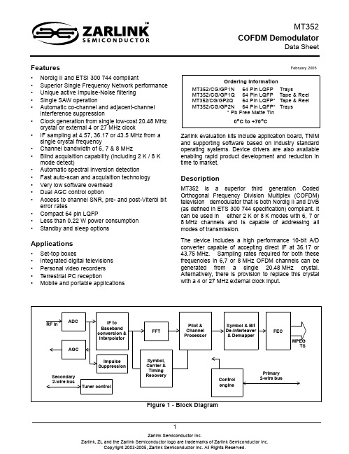
Ordering InformationMT352/CG/GP1N 64 Pin LQFP TraysMT352/CG/GP1Q 64 Pin LQFP Tape & Reel MT352/CG/GP2Q 64 Pin LQFP*Tape & Reel MT352/CG/GP2N 64 Pin LQFP*Trays* Pb Free Matte Tin0o C to +70o CMT352COFDM DemodulatorData SheetFigure 1 - Block DiagramRF inADCAGCSecondary Tuner controlImpulse SuppressionIF to Baseband conversion &InterpolatorFFTSymbol,Carrier &Timing RecoveryPilot &Channel Processor Control engineSymbol & Bit De-interleaver & DemapperFECMPEGTS2-wire busPrimary 2-wire busMT352Data SheetUnique algorithms that actively filter out impulse noise, without affecting normal performance, have been implemented. This reduces the interference effect from vehicles and electrical appliances, which is known to have significant detrimental effect on the quality of digital TV reception.Programming is simplified utilizing a high level command driven interface. A sophisticated engine controls all acquisition and tracking operations as well as controlling the tuner via a 2-wire bus. Any frequency range can be automatically scanned for digital TV channels. This mechanism ensures minimal interaction, maximum flexibility,fastest acquisition and the fastest auto scan capability of any chip in the market.Blind acquisition mode enables automatic detection of all OFDM signal parameters, including mode, guard and spectral inversion. The frequency capture range is sufficient to compensate for the combined offset introduced by the tuner and broadcaster.The device is packaged in a 64 pin LQFP and consumes less than 220mW of power.Figure 2 - Package OutlineMT352 CG YYWW *W ∆•Pin 1 CornerMT352Data Sheet Pin DescriptionPin Description TablePin No Name Description I/O Type V mA MPEG pins47MOSTRT MPEG packet start OCMOS Tristate 3·3148MOVAL MPEG data valid O3·31 49-53, 56-58MDO(0:7)MPEG data bus O3·31 61MOCLK MPEG clock out O3·31 62BKERR Block error O3·31 63MICLK MPEG clock in I CMOS 3·311STATUS Status output O3·31 6IRQ Interrupt output O Open drain56 Control pins4CLK1Serial clock I CMOS55DATA1Serial data I/O Open drain 56 23XTI Low phase noiseoscillatorICMOS24XTO O10SLEEP Device power down I3·3 12, 15-18SADD(4:0)Serial address set I3·344SMTEST Scan mode enable I3·335CLK2/GPP0Serial clock tuner I/OOpen drain 5636DATA2/GPP1Serial data tuner I/O56 42AGC1Primary AGC O56 41AGC2/GPP2Secondary AGC I/O56 43GPP(3)General purpose I/O I/O56 9RESET Device reset I CMOS527OSCMODE Crystal oscillator mode I CMOS3·326PLLTEST PLL analogue test OAnalog inputs30VIN positive input I31VIN negative input ISupply pinsMT352Data Sheet21PLLVDD PLL supplyS 1·822PLLGND S 07, 19, 37, 39, 59, 64CVDD Core logic power S 1·82, 13, 45, 54, VDD I/O ring power S 3·31, 3, 8, 14, 20, 25, 38, 40, 46, 55, 60GND Core and I/O ground S 028AVDD ADC analog supplyS 1·829, 32AGND S 033DVDD ADC digital supply S 1·834DGNDSPin Description Table (continued)Pin NoName Description I/O TypeV mATable of ContentsFeatures . . . . . . . . . . . . . . . . . . . . . . . . . . . . . . . . . . . . . . . . . . . . . . . . . . . . . . . . . . . . . . . . . . . . . . . . . . . . . . . . . 1 Applications . . . . . . . . . . . . . . . . . . . . . . . . . . . . . . . . . . . . . . . . . . . . . . . . . . . . . . . . . . . . . . . . . . . . . . . . . . . . . 1 Description . . . . . . . . . . . . . . . . . . . . . . . . . . . . . . . . . . . . . . . . . . . . . . . . . . . . . . . . . . . . . . . . . . . . . . . . . . . . . . 1 Pin Description . . . . . . . . . . . . . . . . . . . . . . . . . . . . . . . . . . . . . . . . . . . . . . . . . . . . . . . . . . . . . . . . . . . . . . . . . . . 3 1.0 Functional Description . . . . . . . . . . . . . . . . . . . . . . . . . . . . . . . . . . . . . . . . . . . . . . . . . . . . . . . . . . . . . . . . . .81.1 Analogue-to-Digital Converter. . . . . . . . . . . . . . . . . . . . . . . . . . . . . . . . . . . . . . . . . . . . . . . . . . . . . . . . . . .91.2 Automatic Gain Control. . . . . . . . . . . . . . . . . . . . . . . . . . . . . . . . . . . . . . . . . . . . . . . . . . . . . . . . . . . . . . . .91.3 IF to Baseband Conversion. . . . . . . . . . . . . . . . . . . . . . . . . . . . . . . . . . . . . . . . . . . . . . . . . . . . . . . . . . . . .91.4 Adjacent Channel Filtering . . . . . . . . . . . . . . . . . . . . . . . . . . . . . . . . . . . . . . . . . . . . . . . . . . . . . . . . . . . .101.5 Interpolation and Clock Synchronisation. . . . . . . . . . . . . . . . . . . . . . . . . . . . . . . . . . . . . . . . . . . . . . . . . .101.6 Carrier Frequency Synchronisation. . . . . . . . . . . . . . . . . . . . . . . . . . . . . . . . . . . . . . . . . . . . . . . . . . . . . .101.7 Symbol Timing Synchronisation . . . . . . . . . . . . . . . . . . . . . . . . . . . . . . . . . . . . . . . . . . . . . . . . . . . . . . . .101.8 Fast Fourier Transform . . . . . . . . . . . . . . . . . . . . . . . . . . . . . . . . . . . . . . . . . . . . . . . . . . . . . . . . . . . . . . .101.9 Common Phase Error Correction . . . . . . . . . . . . . . . . . . . . . . . . . . . . . . . . . . . . . . . . . . . . . . . . . . . . . . .101.10 Channel Equalisation . . . . . . . . . . . . . . . . . . . . . . . . . . . . . . . . . . . . . . . . . . . . . . . . . . . . . . . . . . . . . . .101.11 Impulse Filtering . . . . . . . . . . . . . . . . . . . . . . . . . . . . . . . . . . . . . . . . . . . . . . . . . . . . . . . . . . . . . . . . . . .101.12 Transmission Parameter Signalling (TPS) . . . . . . . . . . . . . . . . . . . . . . . . . . . . . . . . . . . . . . . . . . . . . . .111.13 De-Mapper. . . . . . . . . . . . . . . . . . . . . . . . . . . . . . . . . . . . . . . . . . . . . . . . . . . . . . . . . . . . . . . . . . . . . . . .111.14 Symbol and Bit De-Interleaving. . . . . . . . . . . . . . . . . . . . . . . . . . . . . . . . . . . . . . . . . . . . . . . . . . . . . . . .111.15 Viterbi Decoder . . . . . . . . . . . . . . . . . . . . . . . . . . . . . . . . . . . . . . . . . . . . . . . . . . . . . . . . . . . . . . . . . . . .111.16 MPEG Frame Aligner . . . . . . . . . . . . . . . . . . . . . . . . . . . . . . . . . . . . . . . . . . . . . . . . . . . . . . . . . . . . . . .111.17 De-interleaver . . . . . . . . . . . . . . . . . . . . . . . . . . . . . . . . . . . . . . . . . . . . . . . . . . . . . . . . . . . . . . . . . . . . .111.18 Reed-Solomon Decoder . . . . . . . . . . . . . . . . . . . . . . . . . . . . . . . . . . . . . . . . . . . . . . . . . . . . . . . . . . . . .111.19 De-scrambler. . . . . . . . . . . . . . . . . . . . . . . . . . . . . . . . . . . . . . . . . . . . . . . . . . . . . . . . . . . . . . . . . . . . . .121.20 MPEG Transport Interface. . . . . . . . . . . . . . . . . . . . . . . . . . . . . . . . . . . . . . . . . . . . . . . . . . . . . . . . . . . .122.0 Software control. . . . . . . . . . . . . . . . . . . . . . . . . . . . . . . . . . . . . . . . . . . . . . . . . . . . . . . . . . . . . . . . . . . . . . .123.0 Interfaces . . . . . . . . . . . . . . . . . . . . . . . . . . . . . . . . . . . . . . . . . . . . . . . . . . . . . . . . . . . . . . . . . . . . . . . . . . . .123.1 2-Wire Bus. . . . . . . . . . . . . . . . . . . . . . . . . . . . . . . . . . . . . . . . . . . . . . . . . . . . . . . . . . . . . . . . . . . . . . . . .133.2 Host. . . . . . . . . . . . . . . . . . . . . . . . . . . . . . . . . . . . . . . . . . . . . . . . . . . . . . . . . . . . . . . . . . . . . . . . . . . . . .133.2.1 Tuner . . . . . . . . . . . . . . . . . . . . . . . . . . . . . . . . . . . . . . . . . . . . . . . . . . . . . . . . . . . . . . . . . . . . . . . .133.2.2 Examples of 2-Wire Bus Messages. . . . . . . . . . . . . . . . . . . . . . . . . . . . . . . . . . . . . . . . . . . . . . . . .143.2.3 Primary 2-Wire Bus Timing . . . . . . . . . . . . . . . . . . . . . . . . . . . . . . . . . . . . . . . . . . . . . . . . . . . . . . .143.3 MPEG . . . . . . . . . . . . . . . . . . . . . . . . . . . . . . . . . . . . . . . . . . . . . . . . . . . . . . . . . . . . . . . . . . . . . . . . . . . .153.3.1 Data Output Header Format. . . . . . . . . . . . . . . . . . . . . . . . . . . . . . . . . . . . . . . . . . . . . . . . . . . . . . .153.3.2 MPEG data output signals. . . . . . . . . . . . . . . . . . . . . . . . . . . . . . . . . . . . . . . . . . . . . . . . . . . . . . . .163.3.3 MPEG Output Timing. . . . . . . . . . . . . . . . . . . . . . . . . . . . . . . . . . . . . . . . . . . . . . . . . . . . . . . . . . . .163.3.3.1 MOCLKINV = 1. . . . . . . . . . . . . . . . . . . . . . . . . . . . . . . . . . . . . . . . . . . . . . . . . . . . . . . . . . . .173.3.3.2 MOCLKINV = 0. . . . . . . . . . . . . . . . . . . . . . . . . . . . . . . . . . . . . . . . . . . . . . . . . . . . . . . . . . . .174.0 Electrical Characteristics . . . . . . . . . . . . . . . . . . . . . . . . . . . . . . . . . . . . . . . . . . . . . . . . . . . . . . . . . . . . . . .194.1 Recommended Operating Conditions. . . . . . . . . . . . . . . . . . . . . . . . . . . . . . . . . . . . . . . . . . . . . . . . . . . .194.2 Absolute maximum ratings . . . . . . . . . . . . . . . . . . . . . . . . . . . . . . . . . . . . . . . . . . . . . . . . . . . . . . . . . . . .194.3 DC Electrical Characteristics . . . . . . . . . . . . . . . . . . . . . . . . . . . . . . . . . . . . . . . . . . . . . . . . . . . . . . . . . .204.4 Crystal Specification and External Clocking . . . . . . . . . . . . . . . . . . . . . . . . . . . . . . . . . . . . . . . . . . . . . . .215.0 Application Circuit. . . . . . . . . . . . . . . . . . . . . . . . . . . . . . . . . . . . . . . . . . . . . . . . . . . . . . . . . . . . . . . . . . . . .22Figure 1 - Block Diagram. . . . . . . . . . . . . . . . . . . . . . . . . . . . . . . . . . . . . . . . . . . . . . . . . . . . . . . . . . . . . . . . . . . . . 1 Figure 2 - Package Outline . . . . . . . . . . . . . . . . . . . . . . . . . . . . . . . . . . . . . . . . . . . . . . . . . . . . . . . . . . . . . . . . . . . 2 Figure 3 - OFDM Demodulator Diagram . . . . . . . . . . . . . . . . . . . . . . . . . . . . . . . . . . . . . . . . . . . . . . . . . . . . . . . . . 8 Figure 4 - FEC Block Diagram. . . . . . . . . . . . . . . . . . . . . . . . . . . . . . . . . . . . . . . . . . . . . . . . . . . . . . . . . . . . . . . . . 8 Figure 5 - Primary Interfaces. . . . . . . . . . . . . . . . . . . . . . . . . . . . . . . . . . . . . . . . . . . . . . . . . . . . . . . . . . . . . . . . . 12 Figure 6 - Primary 2-Wire Bus Timing . . . . . . . . . . . . . . . . . . . . . . . . . . . . . . . . . . . . . . . . . . . . . . . . . . . . . . . . . . 14 Figure 7 - DVB Transport Packet Header Byte . . . . . . . . . . . . . . . . . . . . . . . . . . . . . . . . . . . . . . . . . . . . . . . . . . . 15 Figure 8 - MPEG Output Data Waveforms. . . . . . . . . . . . . . . . . . . . . . . . . . . . . . . . . . . . . . . . . . . . . . . . . . . . . . . 16 Figure 9 - MPEG Timing - MOCLKINV = 1 . . . . . . . . . . . . . . . . . . . . . . . . . . . . . . . . . . . . . . . . . . . . . . . . . . . . . . 17 Figure 10 - MPEG Timing - MOCLKINV = 0 . . . . . . . . . . . . . . . . . . . . . . . . . . . . . . . . . . . . . . . . . . . . . . . . . . . . . 18 Figure 11 - Crystal Oscillator Circuit. . . . . . . . . . . . . . . . . . . . . . . . . . . . . . . . . . . . . . . . . . . . . . . . . . . . . . . . . . . . 21 Figure 12 - Typical Application Circuit . . . . . . . . . . . . . . . . . . . . . . . . . . . . . . . . . . . . . . . . . . . . . . . . . . . . . . . . . . 22Table 1 - Programmable Address Details for 2-Wire Bus in TNIM Evaluation Application. . . . . . . . . . . . . . . . . . . 13 Table 2 - Timing of 2-Wire Bus. . . . . . . . . . . . . . . . . . . . . . . . . . . . . . . . . . . . . . . . . . . . . . . . . . . . . . . . . . . . . . . . 15 Table 3 - MOCLKINV = 1. . . . . . . . . . . . . . . . . . . . . . . . . . . . . . . . . . . . . . . . . . . . . . . . . . . . . . . . . . . . . . . . . . . . 17 Table 4 - MDOSWAP = 0. . . . . . . . . . . . . . . . . . . . . . . . . . . . . . . . . . . . . . . . . . . . . . . . . . . . . . . . . . . . . . . . . . . . 17 Table 5 - MDOSWAP = 1. . . . . . . . . . . . . . . . . . . . . . . . . . . . . . . . . . . . . . . . . . . . . . . . . . . . . . . . . . . . . . . . . . . . 181.0 Functional DescriptionA functional block diagram of the MT352 OFDM demodulator is shown in Figure 3. This accepts an IF analogue signal and delivers a stream of demodulated soft decision data to the on-chip Viterbi decoder. Clock, timing and frequency synchronization operations are all digital and there are no analogue control loops except the AGC. The frequency capture range is large enough for all practical applications. This demodulator has novel algorithms to combat impulse noise as well as co-channel and adjacent channel interference. If the modulation is hierarchical, the OFDM outputs both high and low priority data streams. Only one of these streams is FEC-decoded, but the FEC can be switched from one stream to another with minimal interruption to the transport stream.Figure 3 - OFDM Demodulator DiagramThe FEC module shown in Figure 4 consists of a concatenated convolutional (Viterbi) and Reed-Solomon decoder separated by a depth-12 convolutional de-interleaver. The Viterbi decoder operates on 5-bit soft decisions to provide the best performance over a wide range of channel conditions. The trace-back depth of 128 ensures minimum loss of performance due to inevitable survivor truncation, especially at high code rates. Both the Viterbi and Reed-Solomon decoders are equipped with bit-error monitors. The former provides the bit error rate (BER) at the OFDM output. The latter is the more useful measure as it gives the Viterbi output BER. The error collecting intervals of these are programmable over a very wide range.Figure 4 - FEC Block DiagramThe FSM controller shown in Figure 3 above controls both the demodulator and the FEC. It also drives the 2-wire bus to the tuner. The controller facilitates the automated search of all parameters or any sub-set of parameters of the received signal. It can also be used to scan any defined frequency range searching for OFDM channels. Thismechanism provides the fast channel scan and acquisition performance, whilst requiring minimal software overhead in the host driver.The algorithms and architectures used in the MT352 have been heavily optimized to minimize hardware and chip area. This is proven by its 220mW (typical) power consumption, which is the lowest of any OFDM device in the market today.1.1 Analogue-to-Digital ConverterThe MT352 has a high performance 10-bit analogue-to-digital converter (ADC) which can sample a 6, 7 or 8MHz bandwidth OFDM signal, with its spectrum centred at:• 4.57MHz near-zero IF•36.17MHz IF•43.75MHz IFThe ADC can be clocked using:•Crystal oscillator with a 20.48MHz crystal• 4 MHz or 27MHz clock inputAn on-chip programmable phase locked loop (PLL) is used to generate the ADC sampling clock. The crystal frequency of 20.48MHz is used for 36.17MHz IF sampling and 19.6267MHz is used for 43.75MHz IF sampling. Note that this 19.6267MHz sampling clock can be generated from the 20.48MHz crystal by appropriately programming the PLL. Hence the same 20.48MHz crystal can support 6, 7 and 8MHz OFDM as well as 36.17 and 43.75MHz IF.1.2 Automatic Gain ControlAn AGC module compares the absolute value of the digitized signal with a programmable reference. The error signal is filtered and is used to control the gain of the amplifier. A sigma-delta modulated output is provided, which has to be RC low-pass filtered to obtain the voltage to control the amplifier. Upper and lower limits can be set to the AGC control voltage using registers.The programmable AGC reference has been optimized. A large value for the reference leads to excessive ADC clipping and a small value results in excessive quantization noise. Hence the optimum value has been determined assuming the input signal amplitude to be Gaussian distributed. The latter is justified by applying the central limit theorem in statistics to the OFDM signal, which consists of a large number of randomly modulated carriers. This reference or target value may have to be lowered slightly for some applications. Slope control bits have been provided for the AGCs and these have to be set correctly depending on the Gain-versus-Voltage slope of the gain control amplifiers.The bandwidth of the AGC is set to a large value for quick acquisition then reduced to a small value for tracking. The AGC is free running during OFDM channel changes and locks to the new channel while the tuner lock is being established. This is one of the features of MT352 used to minimize acquisition time. A robust AGC lock mechanism is provided and the other parts of the MT352 begin to acquire only after the AGC has locked. Two AGC control outputs are available, one to drive an RF amplifier and the other to control an IF amplifier. The parameters for both loops are programmable. In the default mode, only the IF AGC loop is activated.1.3 IF to Baseband ConversionSampling a 36.17MHz IF signal at 20.48MHz results in a spectrally inverted OFDM signal centred at 4.79MHz. Sampling a 43.75MHz IF signal at 19.6267MHz gives a non-inverted signal at 4.5MHz. The first step of the demodulation process is to convert this signal to a complex (in-phase and quadrature) signal in baseband. A correction for spectral inversion is implemented during this conversion process. Note also that the MT352 has control mechanisms to search automatically for an unknown spectral inversion status.1.4 Adjacent Channel FilteringAdjacent channels, in particular the Nicam digital sound signal associated with analogue channels, are filtered prior to the FFT.1.5 Interpolation and Clock SynchronisationMT352 uses digital timing recovery and this eliminates the need for an external VCXO. The ADC samples the signal at a fixed rate, for example, 20.48MHz. Conversion of the 20.48MHz signal to the OFDM sample rate is achieved using the time-varying interpolator. The OFDM sample rate is 64/7MHz for 8 MHz and this is scaled by factors 6/8 and 7/8 for 6 and 7MHz channel bandwidths. The nominal ratio of the ADC to OFDM sample rate is programmed in a MT352 register (defaults are for 20.48MHz sampling and 8MHz OFDM). The clock recovery phase locked loop in the MT352 compensates for inaccuracies in this ratio due to uncertainties of the frequency of the sampling clock.1.6 Carrier Frequency SynchronisationThere can be frequency offsets in the signal at the input to OFDM, partly due to tuner step size and partly due to broadcast frequency shifts, typically 1/6MHz. These are tracked out digitally, without the need for an analogue frequency control (AFC) loop.The default frequency capture range has been set to ±285kHz in the 2K mode and ±142kHz in the 8K mode. However, these values can be doubled, if necessary, by programming an on-chip register. It is recommended that this larger capture range be used for channel scan in order to find channels with broadcast frequency shifts, without having to adjust the tuner.After the OFDM module has locked, the frequency offset can be read from an on-chip register.1.7 Symbol Timing SynchronisationThis module computes the optimum sample position to trigger the FFT in order to eliminate or minimize inter-symbol interference in the presence of multi-path distortion. Furthermore, this trigger point is continuously updated to dynamically adapt to time-variations in the transmission channel.1.8 Fast Fourier TransformThe FFT module uses the trigger information from the timing synchronization module to set the start point for an FFT. It then uses either a 2K or 8K FFT to transform the data from the time domain to the frequency domain. An extremely hardware-efficient and highly accurate algorithm has been used for this purpose.1.9 Common Phase Error CorrectionThis module subtracts the common phase offset from all the carriers of the OFDM signal to minimize the effect of the tuner phase noise on system performance.1.10 Channel EqualisationThis consists of two parts. The first part involves estimating the channel frequency response from pilot information. Efficient algorithms have been used to track time-varying channels with a minimum of hardware. The second part involves applying a correction to the data carriers based on the estimated frequency response of the channel. This module also generates dynamic channel state information (CSI) for every carrier in every symbol.1.11 Impulse FilteringMT352 contains several mechanisms to reduce the impact of impulse noise on system performance.1.12 Transmission Parameter Signalling (TPS)An OFDM frame consists of 68 symbols and a superframe is made up of four such frames. There is a set of TPS carriers in every symbol and all these carry one bit of TPS. These bits, when combined, include information about the transmission mode, guard ratio, constellation, hierarchy and code rate, as defined in ETS 300 744. In addition, the first eight bits of the cell identifier are contained in even frames and the second eight bits of the cell identifier are in odd frames. The TPS module extracts all the TPS data, and presents these to the host processor in a structured manner.1.13 De-MapperThis module generates soft decisions for demodulated bits using the channel-equalized in-phase and quadrature components of the data carriers as well as per-carrier channel state information (CSI). The de-mapping algorithm depends on the constellation (QPSK, 16QAM or 64QAM) and the hierarchy α = 0, 1, 2 or 3). Soft decisions for both low- and high-priority data streams are generated.1.14 Symbol and Bit De-InterleavingThe OFDM transmitter interleaves the bits within each carrier and also the carriers within each symbol. The de-interleaver modules consist largely of memory to invert these interleaving functions and present the soft decisions to the FEC in the original order.1.15 Viterbi DecoderThe Viterbi decoder accepts the 5-bit soft decision data from the OFDM demodulator and outputs a decoded bit-stream. The decoder does the de-puncturing of the input data for all code rates other than 1/2. It then evaluates the branch metrics and passes these to a 64-state path-metric updating unit, which in turn outputs a 64-bit word to the survivor memory. The Viterbi decoded bits are obtained by tracing back the survivor paths in this memory. A trace-back depth of 128 is used to minimize any loss in performance, especially at high code rates.The decoder re-encodes the decoded bits and compares these with received data (delayed) to compute bit errors at its input, on the assumption that the Viterbi output BER is significantly lower than its input BER.1.16 MPEG Frame AlignerThe Viterbi decoded bit stream is aligned into 204-byte frames. A robust synchronization algorithm is used to ensure correct lock and to prevent loss of lock due to noise impulses.1.17 De-interleaverErrors at the Viterbi output occur in bursts and the function of the de-interleaver is to spread these errors over a number of 204-byte frames to give the Reed-Solomon decoder a better chance of correcting these. The de-interleaver is a memory unit which implements the inverse of the convolutional interleaving function introduced by the transmitter.1.18 Reed-Solomon DecoderEvery 188-byte transport packet is encoded by the transmitter into a 204-byte frame, using a truncated version of a systematic (255,239) Reed-Solomon code. The corresponding (204,188) Reed-Solomon decoder is capable of correcting up to eight byte errors in a 204-byte frame. It may also detect frames with more than eight byte errors. In addition to efficiently performing this decoding function, the Reed-Solomon decoder in MT352 keeps a count of the number of bit errors corrected over a programmable period and the number of uncorrectable blocks. This information can be used to compute the post-Viterbi BER.1.19 De-scramblerThe de-scrambler de-randomizes the Reed-Solomon decoded data by generating the exclusive-OR of this with a pseudo-random bit sequence (PRBS). This outputs 188-byte MPEG transports packets. The TEI bit of the packet header is set to indicate uncorrectable packets.1.20 MPEG Transport InterfaceMPEG data can be output in parallel or serial mode. The output clock frequency is automatically chosen to present the MPEG data as uniformly spaced as possible to the transport processor. This frequency depends on the guard ratio, constellation, hierarchy and code rate. There is also an option for the data to be extracted from the MT352 with a clock provided by the user.2.0 Software controlAcquisition of an OFDM channel and frequency scan for OFDM channels are controlled by an on-chip state machine, which minimizes the software requirement in the host processor. To acquire a channel, the host programs the channel frequency in the MT352. The on-chip state machine then writes the frequency information to the tuner, awaits tuner lock and acquires the OFDM channel to generate the transport stream. The controller can be made to automatically search for every parameter in the OFDM signal, including spectral inversion status. Furthermore, this controller will re-acquire the channel in the event of an interruption to the incoming signal.To scan a frequency range, the host programs the start and end frequencies for the search as well as the step size, which defaults to 8 MHz. The MT352 then automatically scans the frequency range by appropriately programming the tuner and searching for OFDM signals. Once a channel has been located, the host is interrupted to read the channel information from the MT352. Then MT352 continues the search. By default, only the channels which can generate a reliable transport stream are reported, but there is also provision for locating very weak channels. The frequency capture range of MT352 can be maximized to capture channels with frequency offsets without re-programming the tuner, in both 2K and 8K modes.The above approach to channel acquisition and scan has resulted in very fast acquisition and scan times whilst minimizing software overhead in the host processor. Furthermore, all this functionality has very efficiently been mapped into hardware to result in a device consuming less than 220mW of power.3.0 InterfacesFigure 5 - Primary InterfacesThe MT352 interfaces to other parts of a terrestrial receiver system can be partitioned into three groups: the host controller, the tuner and the MPEG decoder. One other pin, the Status output, is multi-functional and can directlydrive a LED to show the status of a range of different internal lock flags. Alternatively, it can drive an audio transducer to give an audio frequency that is dependent upon the error rate of the received signal.This feature can be used for faster installation of a system where the aerial may need to be adjusted, as signal strength is not the best guide for the optimum aerial position for COFDM reception.3.1 2-Wire Bus3.2 HostThe primary 2-wire bus serial interface uses pins:•DATA1 (pin 5) serial data, the most significant bit is sent first.•CLK1 (pin 4) serial clock.The 2-wire bus address is determined by applying VDD or VSS to the SADD[4:0] pins.In the current TNIM evaluation application, the 2-wire bus address is 0001 111 R/ W with the pins connected as follows:ADDR[7] ADDR[6] ADDR[5] ADDR[4] ADDR[3] ADDR[2] ADDR[1]Not programmable SADD[4] SADD[3] SADD[2] SADD[1] SADD[0]VSS VSS VSS VDD VDD VDD VDD Table 1 - Programmable Address Details for 2-Wire Bus in TNIM Evaluation ApplicationWhen the MT352 is powered up, the RESET pin 28 should be held low for at least 50ms after VDD has reached normal operation levels. As the RESET pin goes high, the logic levels on SADD[4:0] are latched as the 2-wire bus address. ADDR[0] is the R/ W bit.The circuit works as a slave transmitter with the lsb set high or as a slave receiver with the lsb set low. In receive mode, the first data byte is written to the RADD virtual register, which forms the register sub-address. The RADD register takes an 8-bit value that determines which of 256 possible register addresses is written to by the following byte. Not all addresses are valid and many are reserved registers that must not be changed from their default values. Multiple byte reads or writes will auto-increment the value in RADD, but care should be taken not to access the reserved registers accidentally.Following a valid chip address, the 2-wire bus STOP command resets the RADD register to 00. If the chip address is not recognized, the MT352 will ignore all activity until a valid chip address is received. The 2-wire bus START command does NOT reset the RADD register to 00. This allows a combined 2-wire bus message, to point to a particular read register with a write command, followed immediately with a read data command. If required, this could next be followed with a write command to continue from the latest address. RADD would not be sent in this case. Finally, a STOP command should be sent to free the bus.When the 2-wire bus is addressed (after a recognized STOP command) with the read bit set, the first byte read out is the contents of register 00.3.2.1 TunerThe MT352 has a General Purpose Port that can be configured to provide a secondary 2-wire bus. Master control mode is selected by a single register control bit.The allocation of the pins is: GPP0 pin 35 = CLK2, GPP1 pin 36 = DATA2.。
ACS244MS中文资料

1CAUTION: These devices are sensitive to electrostatic discharge; follow proper IC Handling Procedures.1-888-INTERSIL or 321-724-7143|Copyright © Intersil Corporation 1999March 1998ACS244MSRadiation Hardened Non-Inverting,Octal, Three-State Buffer/Line DriverFeatures•QML Qualified Per MIL-PRF-38535 Requirements • 1.25Micron Radiation Hardened SOS CMOS•Radiation Environment-Latch-up Free Under any Conditions-Total Dose. . . . . . . . . . . . . . . . . . . . . .3 x 105RAD(Si)-SEU Immunity. . . . . . . . . . .<1 x 10⁻¹⁰ Errors/Bit/Day -SEU LET Threshold . . . . . . . . . . .>100MeV/(mg/cm 2)•Input Logic Levels .V IL = (0.3V)(V CC ), V IH = (0.7V)(V CC )•Output Current. . . . . . . . . . . . . . . . . . . . . . . . . . .±16mA •Quiescent Supply Current. . . . . . . . . . . . . . . . . . . .20µA •Propagation Delay . . . . . . . . . . . . . . . . . . . . . . . . .9.0nsApplications•Databus Driving •Data Routing•Redundant Data Control CircuitryDescriptionThe Radiation Hardened ACS244MS is a Non-Inverting,Octal, Three-State Buffer/Line Driver with two active-LOW Enable inputs (AE and BE). Each Enable input controls four outputs. When an Enable input is LOW, the corresponding outputs are active. A HIGH on an Enable input causes the corresponding outputs to be high impedance, regardless of the input levels.The ACS244MS is fabricated on a CMOS Silicon on Sap-phire (SOS) process, which provides an immunity to Single Event Latch-up and the capability of highly reliable perfor-mance in any radiation environment. These devices offer significant power reduction and faster performance when compared to ALSTTL types.Specifications for Rad Hard QML devices are controlled by the Defense Supply Center in Columbus (DSCC). The SMD numbers listed below must be used when ordering.Detailed Electrical Specifications for the ACS244 are contained in SMD 5962-98541. A “hot-link” is provided on our homepage with instructions for downloading./data/sm/index.htmOrdering InformationPinoutsACS244 (SBDIP)TOP VIEWACS244 (FLATPACK)TOP VIEWSMD PART NUMBER INTERSIL PART NUMBER TEMP. RANGE (o C)PACKAGE CASE OUTLINE 5962F9854101VRC ACS244DMSR-02-55 to 12520 Ld SBDIP CDIP2-T20N/AACS244D/Sample-022520 Ld SBDIP CDIP2-T205962F9854101VXC ACS244KMSR-02-55 to 12520 Ld Flatpack CDFP4-F20N/A ACS244K/Sample-022520 Ld Flatpack CDFP4-F20N/AACS244HMSR-0225DieN/A1112131415161718201910987654321AE AI1BO4AI2BO3AI3AI4BO2BO1GND V CC AO1BI4AO2BE BI3AO3BI2AO4BI12345678120191817161514139101211AE AI1BO4AI2BO3AI3AI4BO2BO1GNDV CC AO1BI4AO2BE BI3AO3BI2AO4BI1File Number44792All Intersil semiconductor products are manufactured, assembled and tested under ISO9000 quality systems certification.Intersil products are sold by description only. Intersil Corporation reserves the right to make changes in circuit design and/or specifications at any time without notice. Accordingly, the reader is cautioned to verify that data sheets are current before placing orders. Information furnished by Intersil is believed to be accurate and reliable. However, no responsibility is assumed by Intersil or its subsidiaries for its use; nor for any infringements of patents or other rights of third parties which may result from its use. No license is granted by implication or otherwise under any patent or patent rights of Intersil or its subsidiaries.For information regarding Intersil Corporation and its products, see web site Sales Office HeadquartersNORTH AMERICA Intersil CorporationP. O. Box 883, Mail Stop 53-204Melbourne, FL 32902TEL:(321) 724-7000FAX: (321) 724-7240EUROPE Intersil SAMercure Center100, Rue de la Fusee 1130 Brussels, Belgium TEL: (32) 2.724.2111FAX: (32) 2.724.22.05ASIAIntersil (Taiwan) Ltd.Taiwan Limited7F-6, No. 101 Fu Hsing North Road Taipei, Taiwan Republic of ChinaTEL: (886) 2 2716 9310FAX: (886) 2 2715 3029Die CharacteristicsDIE DIMENSIONS:Size:2540µm x 2540µm (100 mils x 100mils)Thickness:525µm ±25µm (20.6 mils ±1 mil)Bond Pad: 110µm x 110µm (4.3 x 4.3 mils)METALLIZATION:AlMetal 1 Thickness: 0.7µm ±0.1µm Metal 2 Thickness: 1.0µm ±0.1µm SUBSTRATE POTENTIAL:Unbiased InsulatorPASSIVATIONType: Phosphorous Silicon Glass (PSG)Thickness: 1.30µm ±0.15µm SPECIAL INSTRUCTIONS:Bond V CC FirstADDITIONAL INFORMATION:Worst Case Density:<2.0 x 10⁵ A/cm 2Transistor Count:214Metallization Mask LayoutACS244MSBO4 (3)AI2 (4)BO3 (5)AI3 (6)BO2 (7)AI4 (8)V CC BO1 (9)AO4 (12)(13)BI2(14)AO3(15)BI3(16)AO2(17)BI4(18)AO1(20)V CC (20)AE (1)AI1(2)BE (19)(11)BI1(10)GND (10)GND ACS244MS。
AOL1718中文资料

元器件交易网
AOL1718
Electrical Characteristics (TJ=25°C unless otherwise noted)
Symbol
Parameter
Conditions
Min Typ Max Units
STATIC PARAMBiblioteka TERS10.7ns
RGEN=3Ω
40
ns
tf
Turn-Off Fall Time
12.5
ns
trr
Body Diode Reverse Recovery Time IF=20A, dI/dt=500A/µs
10
13
16
ns
Qrr
Body Diode Reverse Recovery Charge IF=20A, dI/dt=500A/µs
8
1.0E+02
ID=20A
6
1.0E+4001
125°C
IS (A)
125°C
4
D. The RθJA is the sum of the thermal impedence from junction to case RθJC and case to ambient. E. The static characteristics in Figures 1 to 6 are obtained using <300µs pulses, duty cycle 0.5% max. F. These curves are based on the junction-to-case thermal impedence which is measured with the device mounted to a large heatsink, assuming a maximum junction temperature of TJ(MAX)=175°C. The SOA curve provides a single pulse rating. G. The maximum current rating is limited by bond-wires. H. These tests are performed with the device mounted on 1 in2 FR-4 board with 2oz. Copper, in a still air environment with TA=25°C.
AON6910A;中文规格书,Datasheet资料

VDS ID (at VGS=10V) RDS(ON) (at VGS=10V) RDS(ON) (at VGS = 4.5V)
100% UIS Tested 100% Rg Tested
Q1 30V 37A <14mΩ <20mΩ
Q2 30V 80A <4.1mΩ <5.0mΩ
Top View
DFN5X6B Bottom View
B. The power dissipation P D is based on TJ(MAX)=150°C, using junction-to-case thermal resistance, and is more useful in setting the upper dissipation limit for cases where additional heatsinking is used.
AON6910A
30V Dual Asymmetric N-Channel MOSFET
General Description
Product Summary
The AON6910A is designed to provide a high efficiency synchronous buck power stage with optimal layout and board space utilization.It includes two specialized MOSFETs in a dual Power DFN5x6B package. The Q1 "High Side" MOSFET is desgined to minimze switching losses. The Q2 "Low Side" MOSFET is desgined for low RDS(ON) to reduce conduction losses.Power losses are minimized due to an extremely low combination of RDS(ON) and Crss.In addition,switching behavior is well controlled with a "Schottky style" soft recovery body diode.
- 1、下载文档前请自行甄别文档内容的完整性,平台不提供额外的编辑、内容补充、找答案等附加服务。
- 2、"仅部分预览"的文档,不可在线预览部分如存在完整性等问题,可反馈申请退款(可完整预览的文档不适用该条件!)。
- 3、如文档侵犯您的权益,请联系客服反馈,我们会尽快为您处理(人工客服工作时间:9:00-18:30)。
Product information is current as of publication date. The product conformsCopyright © 2006, 2007, 2009, Pletronics Inc.SM55 SeriesMiniature SMD Crystal January 2009•The Pletronics’ SM55 Series is a miniature surface mount crystal•The package is ideal for automated surface mount assembly and reflow practices.•Tape and Reel packaging• 3 MHz to 70 MHz• 5 x 13 x 5.7 mm 4 pad •AT Cut CrystalPletronics Inc. certifies this device is in accordance with the RoHS 5/6 (2002/95/EC) and WEEE (2002/96/EC) directives.Pletronics Inc. guarantees the device does not contain the following:Cadmium, Hexavalent Chromium, Lead (<1000 ppm), Mercury, PBB’s, PBDE’s Weight of the Device: 0.65 gramsMoisture Sensitivity Level: 1 As defined in J-STD-020C Second Level Interconnect code: e1, e2 or e3Electrical Specification:ItemMin Max Unit Condition Frequency Range370MHz AT cut Calibration Frequency Tolerance --ppm at +25o C +_ 3o Csee table on page 3for available optionsFrequency Stability over OTR --ppm Equivalent Series Resistance (ESR)-200Ohms 3 MHz to 4 MHz Fundamental-150Ohms 4 MHz to 5 MHz -120Ohms 5 MHz to 6 MHz -100Ohms 6 MHz to 7 MHz -80Ohms 7 MHz to 8 MHz -50Ohms 8 MHz to13 MHz -40Ohms 13 MHz to 30 MHz -100Ohms 25 MHz to 70 MHz 3rd Overtone Drive Level-1mW use 10 µW for testing Shunt Capacitance (C0)-7pF Pad to Pad capacitance Aging-5+5ppm /Yrat +25o C +_ 3o CSpecified Temperature Range -40+85o C see table on page 3 for available optionsStorage Temperature Range-55+125oCJanuary 2009Temperature (oC)D e v i a t i o n (p p m )AT Cut Crystal Frequency versus Temperature Typical Performance:Part Marking:1x FFFFF P ymdz or L1x FFFFzywwzLegend:1= Model code for SM55x = Capacitance load code from below FFFFF = Frequency coded P or L = Pletronicsymd or yww = Date of Manufacture (year, month and day) or year, week week All other marking is internal factory codes Some frequency marking examples: 3.579545M = 03579, 14.31818M = 14181, 24.0M = 24000Specifications such as frequency tolerance and operating temperature range, etc. are not identifiedfrom the marking. External packaging labels and packing list will correctly identify the ordered Pletronics part number.Code ABCD EFGHJKLMNPQRSTUVWXYpF1012138151820222426283032343627series 335019161714Codes for Date Code YMDCode 6789012Year 2006200720082009201020112012Code A B C D E F G H J K L M Month JANFEBMARAPRMAY JUN JUL AUG SEP OCT NOV DEC Code 123456789A B C Day 123456789101112Code D E F G H J K L M N P R Day 131415161718192021222324Code T U V W X Y Z Day25262728293031January 2009Part Number:SM55-18-14.31818M-50H1G G-XX See chart below for available optionsInternal code or blankHighest Specified Operating TemperatureA = 40o C G = 70o CB = 45oC H = 75o CC = 50o C J = 80o CD = 55o C K = 85o CE = 60o CF = 65o CLowest Specified Operating TemperatureA = +10o C F = -15o C L = -40o CB = +5oC G = -20o CC = 0o C H = -25o CD = -5o C J = -30o CE = -10o C K = -35o CMode: 1 = Fundamental 3 =3rd OvertoneFrequency Stability See chart belowCalibration Frequency Tolerance15 = +_ 15 ppm at 25o C +_ 3o C20 = +_ 20 ppm at 25o C +_ 3o C30 = +_ 30 ppm at 25o C +_ 3o C (Standard)Frequency in MHzCload in pFParallel Resonance from 09 to 44 pF orSR = Series ResonanceSeries ModelAvailable Frequency Stability versus Temperature in ppmOperating Temperature RangeD E F G H J CODE+_ 10+_ 15+_ 20+_ 30+_ 50+_ 1000 to +45o C CB!!!!!!0 to +50o C CC!!!!!!0 to +60o C CE!!!!!!0 to +70o C CG!!!!STD! -10 to +50o C EC!!!!!! -10 to +60o C EE!!!!!! -10 to +75o C EH!!!!!! -20 to +70o C GG!!!!!! -20 to +75o C GH!!!!!! -30 to +75o C JH!!!!!! -30 to +80o C JJ!!!!!! -30 to +85o C JK!!!!!! -35 to +80o C KJ!!!!! -40 to +85o C LK!!!!!January 2009 Legacy Part Number (not for new designs):SM55B E-18-11.0592M -XXInternal code or blankFrequency in MHzCload in pFParallel Resonance in pF orSR = Series ResonanceOperating Temperature RangeBlank = 0 to + 70o C (STD)E = -40 to +85o CCalibration Tolerance / Frequency StabilityBlank = 30/50 (STD)B = 30/30C = 15/30D = 10/20 (not all frequencies)Series ModelReliability:Environmental ComplianceParameter ConditionMechanical Shock MIL-STD-883 Method 2002, Condition BVibration MIL-STD-883 Method 2007, Condition ASolderability MIL-STD-883 Method 2003Thermal Shock MIL-STD-883 Method 1011, Condition APackage LabelingLabel is 1" x 2.6" (25.4mm x 66.7mm)Label is 1" x 2.6" (25.4mm x 66.7mm) Font is Courier New Font is ArialBar code is 39-Full ASCIIJanuary 2009 Mechanical:Inches mmA0.189 max 4.8 maxB0.512 max13.0 maxC0.224 max 5.7 maxD10.051 1.3E10.3037.7F10.047 1.2Inches mm0.197 max 5.0 maxA10.181 4.6A2B0.516 max13.1 maxC0.224 max 5.7 max10.063 1.6D110.118 3.0D2E10.2807.1F10.039 1.0 Contacts : Matte Tin (Sn) -or- Tin over Copper (SnCu) or SAC (SnAgCu)Layout and application information•Trace lengths to the crystal should be kept as short as possible.•The crystal connections are sensitive to noise.•The package should be grounded for optimum performance.January 2009Tape and Reel: available for quantities of 1000 per reelJanuary 2009IMPORTANT NOTICEPletronics Incorporated (PLE) reserves the right to make corrections, improvements, modifications and other changes to this product at anytime. PLE reserves the right to discontinue any product or service without notice. Customers are responsible for obtaining the latest relevant information before placing orders and should verify that such information is current and complete. All products are sold subject to PLE’s terms and conditions of sale supplied at the time of order acknowledgment.PLE warrants performance of this product to the specifications applicable at the time of sale in accordance with PLE’s limited warranty. Testing and other quality control techniques are used to the extent PLE deems necessary to support this warranty. Except where mandated by specific contractual documents, testing of all parameters of each product is not necessarily performed.PLE assumes no liability for application assistance or customer product design. Customers are responsible for their products and applications using PLE components. To minimize the risks associated with the customer products and applications, customers should provide adequate design and operating safeguards. PLE products are not designed, intended, authorized or warranted to be suitable for use in life support applications, devices or systems or other critical applications that may involve potential risks of death, personal injury or severe property or environmental damage. Inclusion of PLE products in such applications is understood to be fully at the risk of the customer. Use of PLE products in such applications requires the written approval of an appropriate PLE officer. Questions concerning potential risk applications should be directed to PLE.PLE does not warrant or represent that any license, either express or implied, is granted under any PLE patent right, copyright, artwork or other intellectual property right relating to any combination, machine or process which PLE product or services are used. Information published by PLE regarding third-party products or services does not constitute a license from PLE to use such products or services or a warranty or endorsement thereof. Use of such information may require a license from a third party under the patents or other intellectual property of the third party, or a license from PLE under the patents or other intellectual property of PLE.Reproduction of information in PLE data sheets or web site is permissible only if the reproduction is without alteration and is accompanied by associated warranties, conditions, limitations and notices. Reproduction of this information with alteration is an unfair and deceptive business practice. PLE is not responsible or liable for such altered documents.Resale of PLE products or services with statements different from or beyond the parameters stated by PLE for that product or service voids all express and implied warranties for the associated PLE product or service and is an unfair or deceptive business practice. PLE is not responsible for any such statements.Contacting Pletronics Inc.Pletronics Inc.Tel: 425-776-188019013 36th Ave. West Fax: 425-776-2760Lynnwood, WA 98036-5761 USA E-mail: ple-sales@URL: Copyright © 2005, 2006, 2007, 2008, 2009 Pletronics Inc.。