TLC271ACPE4中文资料
CD4584中文资料

4.5
2.0
2.5
3.0 3.5 4.0 4.5 5.0 5.5 OPERATING CURRENT lZT (mA)
6.0
TYPICAL CHANGE OF TEMPERATURE COEFFICIENT WITH CHANGE IN OPERATING CURRENT
10000 5000 10000
22 COREY STREET, MELROSE, MASSACHUSETTS 02176 PHONE (781) 665-1071 FAX (781) 665-7379 WEBSITE: E-mail: mail@
元器件交易网
Backside is not cathode and must be electrically isolated. T = Metallization Test Pad
DESIGN DATA
METALLIZATION: Top: C (Cathode) ...................Al A (Anode) ...................... Al Back: .......................................Au AL THICKNESS.........25,000 Å Min GOLD THICKNESS......4,000 Å Min CHIP THICKNESS. ..............10 Mils CIRCUIT LAYOUT DATA: Backside must be electrically isolated. Backside is not cathode. For Zener operation cathode must be operated positive with respect to anode. TOLERANCES: ALL Dimensions + 2 mils
UPC2714T-E3中文资料

ELECTRICAL CHARACTERISTICS (TA = 25°C, f = 0.5 GHz, VCC = 3.4 V)
PART NUMBER PACKAGE OUTLINE SYMBOLS ICC GS fU ∆GS PSAT NF RLIN RLOUT ISOL ∆GT RTH PARAMETERS AND CONDITIONS Circuit Current Small Signal Gain Upper Limit Operating Frequency (The gain at fU is 3 dB down from the gain at 0.1 GHz) Gain Flatness, f = 0.1~ 0.6 GHz Saturated Output Power Noise Figure Input Return Loss Output Return Loss Isolation Gain-Temperature Coefficient Thermal Resistance (Junction to Ambient) UNITS mA dB GHz dB dBm dB dB dB dB dB/°C °C/W 10 5 22 -10 MIN 3.3 8.5 1.4 UPC2714T T06 TYP 4.5 11.5 1.8 ±1.0 -7 5.0 13 8 27 +0.006 200 6.5 12 5 28 -9 MAX 5.7 15.5 MIN 3.3 16 0.9 UPC2715T T06 TYP 4.5 19 1.2 ±1.0 -6 4.5 17 8 33 +0.006 200 6.0 MAX 5.7 23
-30
-30
-40
-40 0.1 0.3 1.0 2.0
TLC271CPW中文资料

D, JG, OR P PACKAGE (TOP VIEW)
OFFSET N1 IN – IN + GND
1 2 3 4
8 7 6 5
BIAS SELECT VDD OUT OFFSET N2
FK PACKAGE (TOP VIEW)
description
The TLC271 operational amplifier combines a wide range of input offset voltage grades with low NC – No internal connection offset voltage drift and high input impedance. In addition, the TLC271 offers a bias-select mode that allows the user to select the best combination of power dissipation and ac performance for a particular application. These devices use Texas Instruments silicon-gate LinCMOS technology, which provides offset voltage stability far exceeding the stability available with conventional metal-gate processes.
Copyright 2001, Texas Instruments Incorporated
POST OFFICE BOX 655303
• DALLAS, TEXAS 75265
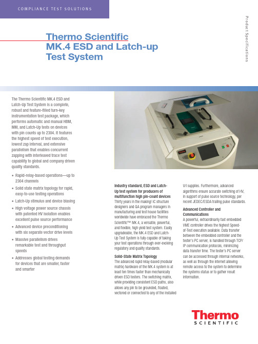
Thermo Scientific MK.4 ESD和Latch-Up测试系统中文名说明书
The Thermo Scientific MK.4 ESD and Latch-Up Test System is a complete,robust and feature-filled turn-key instrumentation test package, which performs automatic and manual HBM, MM, and Latch-Up tests on devices with pin counts up to 2304. It features the highest speed of test execution, lowest zap interval, and extensive parallelism that enables concurrent zapping with interleaved trace test capability to global and company driven quality standards.• Rapid-relay-based operations—up to 2304 channels• Solid state matrix topology for rapid, easy-to-use testing operations • Latch-Up stimulus and device biasing • High voltage power source chassis with patented HV isolation enables excellent pulse source performance • Advanced device preconditioning with six separate vector drive levels • Massive parallelism drives remarkable test and throughput speeds• Addresses global testing demands for devices that are smaller, faster and smarterThermo ScientificMK.4 ESD and Latch-up Test SystemIndustry standard, ESD and Latch-Up test system for producers ofmultifunction high pin-count devices Thirty years in the making! IC structure designers and QA program managers in manufacturing and test house facilities worldwide have embraced the Thermo Scientific™ MK.4, a versatile, powerful, and flexible, high yield test system. Easily upgradeable, the MK.4 ESD and Latch-Up Test System is fully capable of taking your test operations through ever-evolving regulatory and quality standards.Solid-State Matrix TopologyThe advanced rapid relay-based (modular matrix) hardware of the MK.4 system is at least ten times faster than mechanically driven ESD testers. The switching matrix, while providing consistent ESD paths, also allows any pin to be grounded, floated,vectored or connected to any of the installedV/I supplies. Furthermore, advancedalgorithms ensure accurate switching of HV, in support of pulse source technology, per recent JEDEC/ESDA trailing pulse standards.Advanced Controller and CommunicationsA powerful, extraordinarily fast embedded VME controller drives the highest Speed- of-Test execution available. Data transfer between the embedded controller and the tester’s PC server, is handled through TCP/IP communication protocols, minimizing data transfer time. The tester’s PC server can be accessed through internal networks, as well as through the internet allowing remote access to the system to determine the systems status or to gather result information.Product SpecificationsLatch-Up Stimulus and Device Biasing The MK.4 can be equipped with up to eight 100 V four-quadrant Voltage and Current (V/I) power supplies. Each V/I supply has a wide dynamic range enabling it to force and measure very low voltage at high current levels from 100 mV/10 A to 100 V/1 A. The system’s power supply matrix can deliver up to a total of 18A of current, which is distributed between the installed supplies. These supplies are able to provide a fast and versatile means of making DC parametric and leakage measurements as well as providing latch-up pulses, while offering total control and protection of the DUT.Advanced Device PreconditioningThe MK.4 system provides the most advanced device preconditioning capability available. The DUT can be vectored with complex vector patterns, providing excellent control over the device. Each pin can be driven using one of the 6 different vector supplies. The patterns can be up to 256k deep, running at clock speeds of up to 10 MHz. Device conditioning is easily verified, using the read back compare capability available on every pin.Thermo Scientific MK.4 Scimitar™Software Makes Programming Easy, while Providing Unsurpassed Programming FlexibilityThe MK.4 Windows®-based Scimitar operating software empowers users with the flexibility to easily set-up tests based on industry standards or company driven requirements.Device test plans can be created by importing existing text based device files, on the testers PC server or off-line from a satellite PC containing the application. The software also provides the capabilities to import test plans and device files from previous Thermo Scientific test systems.Test vectors from your functional testers can also be imported into the application. And of course, the vector application allows manual creation and debug of vector files.Device test plans and results are stored in an XML data base, providing unsurpassed results handling, sorting and data mining capabilities.Parallelism Drives Remarkable Test Throughput SpeedsThe MK.4 software enables ESD testing of up to twelve devices at one time using the multisite pulse source design.Embedded VME power supplies eliminate any communication delays that would be seen by using stand alone supplies. The embedded parametric (curve tracing) supply also provides fast, accurate curve tracing data to help you analyze your devices performance.The systems curve tracer can also be used as a failure analysis tool by allowing the comparison of stored, known good results, versus results from a new test sample or samples.Ready for Today’s Component Reliability Demands and Anticipating Those to Come ESD and Latch-Up testing of electronic and electrical goods can be very expensive aspects of the design and manufacturing process. This is especially true as market demands for products that are smaller, faster and smarter become the standard rather than the exception. The Thermo Scientific MK.4 leverages the technology and know- how gained over three decades of test system experience, as well as our in-depth participation and contributions to global regulatory bodies governing these changes, enabling today’s products to meet both global and industry-driven quality standards.The real key to our customers’ success is in anticipating what’s next. And to ensure that our customers possess the ability to evolve quickly to meet all change factors with efficiency and cost effectiveness.As such, the strategically-designed, field upgradeable architecture of the MK.4 system ensures a substantial return on investment over a very considerable test system lifecycle, as well as better short- and long-term qualityand ESD and Latch-Up test economies.Custom fixtures include universal package adaptors to enable the industry’s lowest cost-in-service high pin count device fixturing yetdevised. (2304-pin, Universal 1-mm pitch BGA package adaptor shown.)100W V/I Performance Thermo Scientific MK.4: eight-V/I configuration. Powerful V/Is can deliver a total of 800 W to the DUT, enabling complex testing of all advanced high power processors on your product roadmap.Solid state matrix topology for rapid, easy-to-use testing operations. Design ensures waveform integrity and reproducibility.General SpecificationsHuman Body Model (HBM) per ESDA/JEDEC JS-001-2014, MIL-STD 883E, and AEC Q100-002 25 V to 8 kV in steps of 1 V Test to multiple industry standards in one integrated system; no changing or alignment of pulse sources.Wizard-like prompts on multi-step user actions MachineModel (MM) per ESDA STM5.2, JEDEC/JESD22-A115, andAEC Q100-003, 25 V to 1.5 kV in steps of 1 VIntegrated pulse sources allow fast multi-site test execution.Latch-up testing per JEDEC/JESD 78 test pin and AECQ100-004Includes preconditioning, state read-back and full control of each.Rapid Relay-based operations at least 10 times faster thanrobotic-driven testersSuper fast test speeds.Test devices up to 2304 pins Systems available configured as 1152, 1728 or 2304 pins.Waveform network: Two, 12 site HBM (100 pF/1500Ω)and MM (200 pF/0Ω) pulse sources address up to 12devices simultaneouslyPatented design ensures waveform compliance for generations to come.Multiple device selection When multiple devices are present; graphical display indicates the devices selectedfor test; progress indicator displays the current device under test (DUT), along withtest status information.Unsurpassed software architecture Flexible programming, easy to use automated test setups, TCP/IP communication. Enables use of device set-up information Increased efficiency and accuracy from other test equipment, as well as deviceinformation import.Event trigger output Manages setup analysis with customized scope trigger capabilities.High voltage power supply chassis Modular chassis with patented HV isolation enables excellent pulse sourceperformance.Power supply sequencing Provides additional flexibility to meet more demanding test needs of integratedsystem-on-chip (SOC) flexibility.Manages ancillary test equipment through Plug-n feature allows the user to control external devices, such as scopes or heatstreams or other devices the Scimitar Plug-ins feature as required for automatedtesting.Pin drivers for use during Latch-Up testing Vector input/export capability from standard tester platforms and parametricmeasurements.256k vectors per pin with read-back Full real-time bandwidth behind each of the matrix pins.Six independent vector voltage levels Test complex I/O and Multi-Core products with ease.Up to 10MHz vector rate (programmable) Quickly and accurately set the device into the desired state for testing from an internalclock.Comprehensive engineering vector debug. Debug difficult part vectoring setups with flexibility.Up to eight separate V/I supplies (1 stimulus and 7 bias supplies) capability through the V/I matrix High accuracy DUT power, curve tracing, and Latch-up stimulus available; design also provides high current.Low resolution/high accuracy parametric measurements, using an embedded Keithley PSU With the optional Keithley PSU feature (replaces one V/I, nA measurements are achievable, allowing supply bus resistance measurement analysis to be performed.Multiple self-test diagnostic routines Ensures system integrity throughout the entire relay matrix, right up to the test socket Test reports: pre-stress, pre-fail (ESD) and post-fail data,as well as full curve trace and specific data pointmeasurementsData can be exported for statistical evaluation & presentation.Individual pin parametrics Allows the user to define V/I levels, compliance ranges, and curve trace parametersfor each pin individually.Enhanced data set features Report all data gathered for off-line reduction and analysis; core test data is readilyavailable; all data is stored in an easy-to-manipulate standard XML file structure. Interlocked safety cover Ensures no user access during test. All potentially lethal voltages are automaticallyterminated when cover is opened. Safety cover window can be easily modified toaccept 3rd party thermal heads.Dimensions60 cm (23.5 in) W x 99 cm (39 in) D x 127 cm (50 in) H© 2016 Thermo Fisher Scientific Inc. All rights reserved. Windows is a registered trademark of Microsoft Corporation in the United States and/or other countries. All other trademarks are the property of Thermo Fisher Scientific and its subsidiaries. Results may vary under different operating conditions. Specifications, terms and pricing are subject to change. Not all products are available in all countries. Please consult your local sales representative for details.Africa-Other +27 11 570 1840 Australia +61 2 8844 9500 Austria +43 1 333 50 34 0 Belgium +32 53 73 42 41 Canada +1 800 530 8447 China +86 10 8419 3588 Denmark +45 70 23 62 60 Europe-Other +43 1 333 50 34 0Finland /Norway/Sweden+46 8 556 468 00France +33 1 60 92 48 00Germany +49 6103 408 1014India +91 22 6742 9434Italy +39 02 950 591Japan +81 45 453 9100Latin America +1 608 276 5659Middle East +43 1 333 50 34 0Netherlands +31 76 579 55 55South Africa +27 11 570 1840Spain +34 914 845 965Switzerland +41 61 716 77 00UK +44 1442 233555USA +1 800 532 4752Thermo Fisher Scientific,San Jose, CA USA is ISO Certified. CTS.05102016Product SpecificationsScimitar Software FeaturesSummary Panel with easy navigation among device componentsWizard-like prompts on multi-step user actionsControl of external devices through the use of Scimitar’s user programmable Plug-in capabilities, in addition to the Event Trigger Outputs, which provide TTL control signals for external devices, such as power supplies or for triggering oscilloscopesFlexible parametric tests that are defined and placed at an arbitrary position within the executable test plan.Comprehensive results viewer that provides:• ESD and Static Latch-up data viewing capabilities• Curves viewer with zooming capabilities and the ability to add user comments• Data filtering on the following criteria – failed pins, failed results, final stress levels• A complete set or subset of results using user defined parameters• Sorting in ascending or descending order by various column criteriaTree-like logical view of the tests and test plans.Flexible data storage that provides the ability for the end-user to query the dataSeamless support of existing ZapMaster, MK.2, MK.4, and Paragon test plansCurve tracing with curve-to-curve and relative spot-to-spot comparisonOff-line curve analyzing, including third-party generated waveformsCanned JESD78A test (static latch-up only) that can be defined automaticallyPause/Resume test capabilitiesIntermediate results viewingAutomated waveform capture capability and analysis using the embedded EvaluWave software feature。
EPI6L2172KSP45L中文资料

TEL: (818) 892-0761 FAX: (818) 894-5791
---
54
---
40
---
34
---
35
---
40
42
---
38
---
34
---
37
---
37
---
37
---
40
---
Package B20
.330 (8.83)
PCA EPIXXXXXXB20
D.C.
.330 (8.38)
.060 (1.52)
.300 (7.62)
Suggested Pad Latout
元器件交易网
Surface Mount Power Inductor
ELECTRONICS INC.
EPI B30 Series
• Optimized for National’s LM259X Series • Low loss material ensures operation in high frequency switching
converters, such as Buck, Boost or as output averaging filter inductor • Also suitable for use in high quality filter applications • 150 KHz & 500 KHz Switching Frequency • Low Cost Inductor
PZ72L-E4安装使用说明书

仪表量程 电能清零 密码 保存
注: 1、电能清零操作需在闪动的“ ”下,按动左或右键,使其变为“ 电能清零操作不需另行保存即可生效,且不能恢复,请谨慎操作; 2、百分量是指相对于额定量程计算。
4.3 编程流程 4.3.1 正常显示界面(按动左键或右键,显示界面将按以下顺序进行切换, )
相电压
右键 左键 右键 左键
正常测量时,若有报警产生,则对应的显示数据会闪烁。如果 Prog 菜单中的 do2.U 设置为 AL, 则报警时会在继电器 DO2 上产生一个输出(继电器常开结点闭合) ; 报警显示中只显示 3 个报警状态,但通过通讯方法可读取全部的报警状态; 报警状态可通讯读取,见通讯参量地址表; 报警功能设置,参数见 4.2 菜单符号及意义,设置流程见 4.3.4 Prog 菜单; 报警功能默认为关闭状态,除非客户要求。
4.3.2 主菜单切换(在正常显示画面时,按 SET 键,如下: )
正常状态 rEAd 说明: rEAd — 只读菜单,在此页面,按回车键进入; Prog — 编程菜单,在此页面,按回车键进入; 4.3.3 rEAd 工作参数查看菜单
Prog
说明: 此 rEAd 菜单可按左移、右移键查看设置的各种参数。 按 SET 键返回上一级。
0.5-20.0(分辨率 0.1s)
继电器 1 闭合持续时间(s) 0~20(分辨率 1s) 继电器 2 闭合持续时间(s) 0:继电器工作在保持状态 继电器 2 的用法 电压量程(只读) 电流量程(只读) 电能清除 编程保护密码 询问是否保存 io:作开关量 (K) ; AL:作报警输出(J) 0~400 0~5.0 见注 1 0000~9999 按“回车”保存并退出 按“SET”放弃保存并退出 ” ,然后按动确认键。
EP1C6Q240I7N中文资料(Altera)中文数据手册「EasyDatasheet - 矽搜」

更改摘要
— — — — — —
1–3
初稿
使用该设备插脚引线对于一个给定包所有计划中密度引脚
输入识别哪些I / O引脚可以迁移.在Quartus
® II
软件可以自动交叉引用和地点所有引脚你
当给定一个设备迁移列表.如果一个设备有电源或地 销,但这些相同引脚是不同装置,其在对用户I / O 迁移路径,Quartus II软件防护证销不作为 用户I / O在Quartus II软件.确防护这些引脚连接
100-Pin TQFP
0.5 256 16×16
144-Pin TQFP
0.5 484 22×22
240-Pin PQFP
0.5 1,024 34.6×34.6
256-Pin FineLine
BGA
1.0
289
17×17
324-Pin FineLine
BGA
1.0
361
19×19
400-Pin FineLine
1–2
初稿
2008年 5月
芯片中文手册,看全文,戳
文档修订历史记录
到电路板上相应平面. Quartus II软件储备 I / O引脚所必需与在同一个包有多个电源引脚较大密度布局电源引 脚.
表 1-3.旋风 QFP和 BGAFineLine包装规格
尺度
间距(mm) 区(毫米 ) 长短 × width (mm × mm)
高达288千位RAM.有这样锁相环路(PLL),用于时钟和一个专用双倍数据
速率(DDR)接口,以满足DDR SDRAM和快速周期RAM(FCRAM)内存需求特
点,Cyclone器件可用于数据通道应用提供具有成本效益解决
方案. Cyclone器件支持多种I / O标准,包括LVDS数据速率高达每
FPGA可编程逻辑器件芯片EP4CE115F29C8L中文规格书

Mode 0 (continuous frame mode) is popular for camera pipe operation. Often, the camera pipe is enabled statically, and updates to the coefficients are only required from time to time. On demand software may enable the configuration DMA in stop mode to trigger the fetch of one single BCL. In this mode, the PVP_IPFn_TAG register is useful to match status results with a respective configuration. The new BCL only updates coefficients of processing blocks. The BCL does not alter the pipe configuration.Mode 1 (back-to-back mode) is useful in camera pipe mode when coefficients have to change every N th frame. This mode supports on-the-fly reprogramming of coefficients, but it does not support on-the-fly reprogramming of pipe configurations. The following settings must not change unless the DRAIN bit is set:•Pipe structure (PVP_xxx_CFG registers)•Fundamental operating modes (such as 1st-derivative to 2nd-derivative mode of PEC)•Input format and OPORT configuration (PVP_IPFn_CTL registers)•Horizontal size of input frame (HCNT)If any of the above settings change on-the-fly, the PVP_IPFn_PIPECTL.DRAIN bit must be set for proper operation to use Mode 2. In memory pipe mode, the PVP_IPFn_PIPECTL.DRAIN bit causes of few clock cycles of overhead depending to pipeline depth. In camera pipe mode, the PVP_IPFn_PIPECTL.DRAIN bit causes the loss of an entire frame. Operation stops after the pipe has been drained and resumes with the next incoming VSYNC signal.Whenever the next PVP job stalls until the completion event of the data output DMA is flagged either as an interrupt or as a system trigger, setting the PVP_IPFn_PIPECTL.DRAIN bit is a requirement at the appli-cation level. The data output DMA work unit does not complete as long as related data sticks in the pipe. The data in the pipe does not progress until the configuration DMA and data source grant. Such deadlock situations can be avoided by using Mode 2. Once a deadlock occurs, it can be resolved by Mode 3 opera-tion.Mode 3 (drain now instruction) is more similar to a one-time instruction than an operating mode. This mode is used whenever software needs to respond to unpredictable events. For example, while the camera >01Mode 2: Auto-Completion ModeFCNT frames are requested by the IPFn, and these feed the pipe. The last datawords are automatically pushed out, and the operation automatically completes.If a new configuration is granted by DMA or by MMR writes, the configuration isapplied for the next FCNT set of frames.All processing blocks auto-disable. A new configuration must set all wanted STARTbits again.01Mode 3: Drain Now InstructionThis combination instructs the IPFn to flush all content out of the pipe.All processing blocks auto-disable. A new configuration must set all wanted STARTbits again.Table 30-47:Operating Modes by FCNT and DRAIN Selections (Continued)FCNT DRAINModeConfiguring with Daisy Chain MethodConfiguration and coefficient memory mapped registers (MMRs) of all processing blocks are double buff-ered. Whenever PVP_IPFn_FCNT is zero and the PVP_IPF0_CFG.START and PVP_IPF1_CFG.START bits =1, the values are copied from MMR registers into application buffers at the frame boundary. Due to the pipe-lined nature of the PVP, not all values are copied at the same time. Rather, the timing of value copying is closely related to how the VSYNC of the next frame progresses through the pipe. New settings apply to the first pixel of the new frame immediately after the last pixel of the old frame has been processed. The update command is daisy chained through the pipe, starting from the IPFn blocks through to the OPFn blocks. While sequencing through the daisy chain operation, hardware clears the PVP_xxx_CFG.START bits of all involved processing blocks in MMR space. Write conflicts can occur if software attempts to write the PVP_xxx_CFG registers during the daisy chain operation.The PVP_STAT register provides two status bits that report whether a daisy chain operation is ongoing in the camera pipes (PVP_STAT.CPDC ) or in the memory pipe (PVP_STAT.MPDC ). These bits are set along with the PVP_IPF0_CFG.START or PVP_IPF1_CFG.START bit and are cleared if the output formatters have been updated.In camera pipe mode, the PVP_STAT.CPDC bit is cleared only after the daisy chain progresses through the furthest of the enabled OPFn blocks. During this time, software should not write the PVP registers. If soft-ware mistakenly does write to these registers, the event is reported by the PVP_STAT.CPWRERR and PVP_STAT.MPWRERR flags. While all status bits in the PVP_STAT register are self clearing, the PVP_ILAT register latches the events until cleared by a software handshake.A PVP block which is enabled in either the camera pipe or memory pipe can be moved to the other pipe only after the drain done command is received for the former pipe. This restriction ensures that the PVP completely processes all the pixels in one pipe and disables the PVP block, before the PVP is enables the PVP block for pixel processing in the next pipe.NOTE :Camera pipes and memory pipes can be configured by MMR writes or BCL fetches. These are sepa-rate control mechanisms and are not intended to be mixed for a given pipe during ongoing opera-tion. Before switching from one method to the other, inspect the daisy chain and drain status bits in the PVP_STAT register to ensure no operation from the other method is pending.PMA5ACU7PEC2x HCNT + 11 if 2nd derivative mode with ZCRSS=0, otherwise 1xHCNT + 6IIMn6UDS varies with settingsTable 30-48:Block Latencies (Continued)PVP Block Latency [Data Clocks]P IPELINED V ISION P ROCESSOR (PVP)P ROGRAMMING M ODELto handle the three data flows, BCS, data IN, data OUT, and optionally status data OUT. If the descrip-tors are all completed by the core, multiple PVP memory pipe jobs can be chained without any further core intervention as the DMA operations run through the chained lists and handle the multiple dataflows autonomously. The following description assumes the memory pipe is inactive, (a non initialized state PVP_CTL.MPEN =0).To run a PVP memory pipe job from the PVP memory pipe job list, the PVP first loads the memorypipe configuration into the respective shadow registers of the respective PCP elements to build the PVP memory pipe. The configuration within the shadow register is activated (transferred from shadowregister to active register) using hardware triggers (staggered transfer). This configuration stream into the shadow registers is handled by DMA 45 which is controlled by a linked descriptor list. The last valid descriptor must contain a DMA_CFG.FLOW field =0 (STOP Mode) to gracefully stop the DMA 45 aftercompleting the PVP memory pipe job list and avoid loading non valid data into PVP memory pipeconfiguration register. All DMA_CFG descriptor fields within the linked list have DMA_CFG.FLOW =6 or =7 (descriptor list mode) or alternatively DMA_CFG.FLOW =4 (descriptor array mode).A 1-dimensional DMA operation is shown in the following figure. Note however, a 2-dimensionalDMA operation can also be used.Figure 30-55:Static Linked Descriptor List for Configuration Data (BCL Data)•Job List Global TriggerAfter the first initialization of the linked descriptor list the parameter registers of DMA 45 have to beinitialized, particularly the DMA_DSCPTR_NXT and DMA_CFG register. The DMA 45 is started but thenstalls until the PVP memory pipe is enabled and the PVP_IPFn_FCNT =0.To generate a unique synchronization signal that synchronizes the Data Out (DMA 42) and Data In(DMA 43) stream, all DMA_CFG descriptor fields of DMA 45 should have the bit field DMA_CFG.TRIG =1.This generates a trigger signal after a new configuration is loaded into the shadow registers.•Job List StartAfter setting up the three DMA linked lists, the memory pipe has to be activated (PVP_CTL.MPEN =1).。
- 1、下载文档前请自行甄别文档内容的完整性,平台不提供额外的编辑、内容补充、找答案等附加服务。
- 2、"仅部分预览"的文档,不可在线预览部分如存在完整性等问题,可反馈申请退款(可完整预览的文档不适用该条件!)。
- 3、如文档侵犯您的权益,请联系客服反馈,我们会尽快为您处理(人工客服工作时间:9:00-18:30)。
NC IN – NC IN + NC
4 5 6 7 8
3 2 1 20 19 18 17 16 15 14 9 10 11 12 13
NC OFFSET N1 NC BIAS SELECT NC NC VDD NC OUT NC
PACKAGE CHIP CARRIER (FK) — CERAMIC DIP (JG) —
元器件交易网
TLC271, TLC271A, TLC271B LinCMOS PROGRAMMABLE LOW-POWER OPERATIONAL AMPLIFIERS
SLOS090D – NOVEMBER 1987 – REVISED MARCH 2001
D D
D D D D D D
0°C to 70°C
– 40°C to 85°C – 55°C to 125°C
— TLC271MFK
TLC271MJG
The D package is available taped and reeled. Add R suffix to the device type (e.g., TLC271BCDR).
Copyright 2001, Texas Instruments Incorporated
POST OFFICE BOX 655303
• DALLAS, TEXAS 75265
NC GND NC OFFSET N2 NC
—1Βιβλιοθήκη 元器件交易网TLC271, TLC271A, TLC271B LinCMOS PROGRAMMABLE LOW-POWER OPERATIONAL AMPLIFIERS
SLOS090D – NOVEMBER 1987 – REVISED MARCH 2001
DEVICE FEATURES PARAMETER† PD SR Vn B1 BIAS-SELECT MODE HIGH 3375 3.6 25 1.7 MEDIUM 525 0.4 32 0.5 170 LOW 50 0.03 68 0.09 480 UNIT µW V/µs nV/√Hz MHz V/mV
AVAILABLE OPTIONS TA VIOmax AT 25°C 2 mV 5 mV 10 mV 2 mV 5 mV 10 mV 10 mV SMALL OUTLINE (D) TLC271BCD TLC271ACD TLC271CD TLC271BID TLC271AID TLC271ID TLC271MD PLASTIC DIP (P) TLC271BCP TLC271ACP TLC271CP TLC271BIP TLC271AIP TLC271IP TLC271MP
D D
Input Offset Voltage Drift . . . Typically 0.1 µV/Month, Including the First 30 Days Wide Range of Supply Voltages Over Specified Temperature Range: 0°C to 70°C . . . 3 V to 16 V – 40°C to 85°C . . . 4 V to 16 V – 55°C to 125°C . . . 5 V to 16 V Single-Supply Operation Common-Mode Input Voltage Range Extends Below the Negative Rail (C-Suffix and I-Suffix Types) Low Noise . . . 25 nV/√Hz Typically at f = 1 kHz (High-Bias Mode) Output Voltage Range Includes Negative Rail High Input Impedance . . . 1012 Ω Typ ESD-Protection Circuitry Small-Outline Package Option Also Available in Tape and Reel Designed-In Latch-Up Immunity
bias-select feature
The TLC271 offers a bias-select feature that allows the user to select any one of three bias levels depending on the level of performance desired. The tradeoffs between bias levels involve ac performance and power dissipation (see Table 1). Table 1. Effect of Bias Selection on Performance
D, JG, OR P PACKAGE (TOP VIEW)
OFFSET N1 IN – IN + GND
1 2 3 4
8 7 6 5
BIAS SELECT VDD OUT OFFSET N2
FK PACKAGE (TOP VIEW)
description
The TLC271 operational amplifier combines a wide range of input offset voltage grades with low NC – No internal connection offset voltage drift and high input impedance. In addition, the TLC271 offers a bias-select mode that allows the user to select the best combination of power dissipation and ac performance for a particular application. These devices use Texas Instruments silicon-gate LinCMOS technology, which provides offset voltage stability far exceeding the stability available with conventional metal-gate processes.
PRODUCTION DATA information is current as of publication date. Products conform to specifications per the terms of Texas Instruments standard warranty. Production processing does not necessarily include testing of all parameters.
AVD 23 † Typical at VDD = 5 V, TA = 25°C
description (continued)
Using the bias-select option, these cost-effective devices can be programmed to span a wide range of applications that previously required BiFET, NFET, or bipolar technology. Three offset voltage grades are available (C-suffix and I-suffix types), ranging from the low-cost TLC271 (10 mV) to the TLC271B (2 mV) low-offset version. The extremely high input impedance and low bias currents, in conjunction with good common-mode rejection and supply voltage rejection, make these devices a good choice for new state-of-the-art designs as well as for upgrading existing designs. In general, many features associated with bipolar technology are available in LinCMOS operational amplifiers, without the power penalties of bipolar technology. General applications such as transducer interfacing, analog calculations, amplifier blocks, active filters, and signal buffering are all easily designed with the TLC271. The devices also exhibit low-voltage single-supply operation, making them ideally suited for remote and inaccessible battery-powered applications. The common-mode input voltage range includes the negative rail. A wide range of packaging options is available, including small-outline and chip-carrier versions for high-density system applications. The device inputs and output are designed to withstand – 100-mA surge currents without sustaining latch-up. The TLC271 incorporates internal ESD-protection circuits that prevent functional failures at voltages up to 2000 V as tested under MIL-STD-883C, Method 3015.2; however, care should be exercised in handling these devices as exposure to ESD may result in the degradation of the device parametric performance. The C-suffix devices are characterized for operation from 0°C to 70°C. The I-suffix devices are characterized for operation from – 40°C to 85°C. The M-suffix devices are characterized for operation over the full military temperature range of – 55°C to 125°C.