DRA240-48A中文资料
Eaton XLR-48超级电容器技术数据手册(2023年7月版)说明书
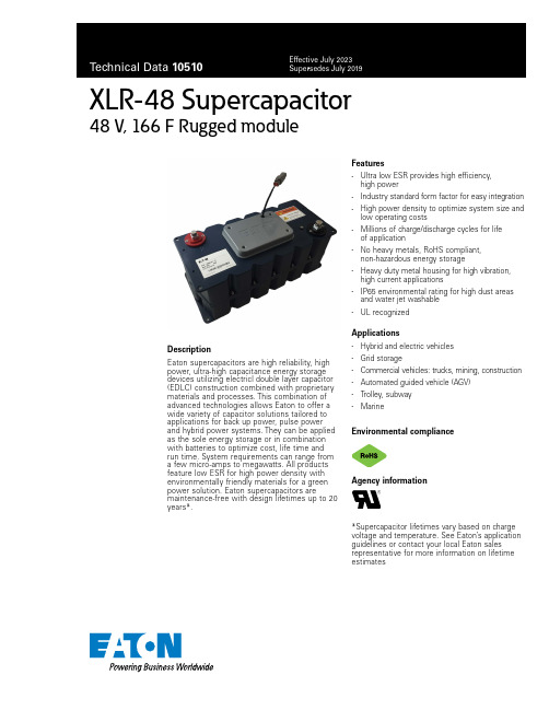
XLR-48 Supercapacitor48 V, 166 F Rugged moduleDescriptionEaton supercapacitors are high reliability, high power, ultra-high capacitance energy storage devices utilizing electricl double layer capacitor (EDLC) construction combined with proprietary materials and processes. This combination of advanced technologies allows Eaton to offer a wide variety of capacitor solutions tailored to applications for back up power, pulse power and hybrid power systems. They can be applied as the sole energy storage or in combination with batteries to optimize cost, life time and run time. System requirements can range from a few micro-amps to megawatts. All products feature low ESR for high power density with environmentally friendly materials for a green power solution. Eaton supercapacitors aremaintenance-free with design lifetimes up to 20 years*.Features•Ultra low ESR provides high efficiency, high power• Industry standard form factor for easy integration •High power density to optimize system size and low operating costs•Millions of charge/discharge cycles for life of application•No heavy metals, RoHS compliant, non-hazardous energy storage•Heavy duty metal housing for high vibration, high current applications•IP65 environmental rating for high dust areas and water jet washable •UL recognizedApplications• Hybrid and electric vehicles • Grid storage• Commercial vehicles: trucks, mining, construction • Automated guided vehicle (AGV)• Trolley, subway •MarineEnvironmental complianceAgency information*Supercapacitor lifetimes vary based on charge voltage and temperature. See Eaton’s application guidelines or contact your local Eaton sales representative for more information on lifetime estimates2Technical Data 10510Effective July 2023XLR-48 Supercapaci tor 48 V, 166 F Rugged module/electronicsRatingsCapacitance166 F Maximum working voltage 48.6 V Surge voltage 51.3 VCapacitance tolerance -0% to 20% (+20 °C)Operating temperature range -40 °C to +65 °CExtended temperature range-40 °C to +85 °C (with linear derating to 41.0 V @ +85 °C)SpecificationsCapacitance 1 (F)Part numberMaximum initial ESR 1 (mΩ)Nominal leakage current 2 (mA)Stored energy 3(Wh)Peak power 4(kW)Pulse current 5(A)Continuous current 6 (A)Typical thermal resistance 7Rth (°C/W)Short circuitcurrent 8 (A)166XLR-48R6167-R 5 5.2541182200860.49700PerformanceParameter (F)Capacitance change (% of initial value)ESR (% of maximum initial value)Life (1500 hours @ +65 °C, 48.6 Vdc)≤ 20%≤ 200%Storage (3 years, uncharged, <+35 °C)≤ 5%≤ 10%Cycle Life 9 (1,000,000 cycles)≤ 20%≤ 200%1. Capacitance and Equivalent series resistance (ESR) measured according to IEC62391-1 at +20 °C, with current in milliamps (mA) = 8*C*V2. Leakage current at +20 °C after 72 hour charge and hold3. Energy (Wh) = ½*C*V 2 36004. Peak power (W) = V 2 4*ESR5. Pulse Current in Amps (A), 1 second discharge from rated voltage to half rated voltage = ½*C*V (1+ESR*C)6. Continuous current with a 15 °C temperature rise. Continuous current (A) =8. Short circuit current is for safety information only. Do not use as operating current.9. Cycling between rated voltage and half voltage, 3 seconds rest at +25 °C10.Testing and verification of product under end application conditions is recommendedSafety and certificationsRegulatory UL 810A, file number MH46887, E-mark (UN-ECE Regulation 10 - Rev. 5 & UN-ECE Regulation 100 - Rev. 2)Shock and vibration IEC 61373 Cat. 1, Class B, SAE J2380, ISO16750-3 Table 14, SAE J2464Warnings Do not overvoltage, do not reverse polarity.Environmental IP65, RoHSShippingUN3499, <10 Wh, Non-hazardous when shipped with shorting wire.EatonElectronics Division 1000 Eaton Boulevard Cleveland, OH 44122United States/electronics© 2023 EatonAll Rights Reserved Printed in USAPublication No. 10510 PCN21003 July 2023Life Support Policy: Eaton does not authorize the use of any of its products for use in life support devices or systems without the express writtenapproval of an officer of the Company. Life support systems are devices which support or sustain life, and whose failure to perform, when properly used in accordance with instructions for use provided in the labeling, can be reasonably expected to result in significant injury to the user.Eaton reserves the right, without notice, to change design or construction of any products and to discontinue or limit distribution of any products. Eaton also reserves the right to change or update, without notice, any technical information contained in this bulletin.Technical Data 10510Effective July 2023XLR-48 Supercapacitor 48 V, 166 F Rugged module Eaton is a registered trademark.All other trademarks are property of their respective owners.Follow us on social media to get thelatest product and support information.Dimensions (mm) and Mass (kg)Part numberL ±1.0L1 ±1.0W ±1.0W1 ±1.0H ±1.0H1 ±1.0H2 ±1.0Typical mass (kg)XLR-48R6167-R 419.5396.2194.5170.0177.0146.5157.014.7Part numbering systemXLR-48R6167-RFamily code Voltage (V)R = decimal Capacitance (μF)Standrd productValueMultiplierXLR = Family code48R6 = 48.6 VExample 16 = 16.6 x 10⁷ (μF) or 166 FPackaging information•Standard packaging: 1piece per boxPart marking• Manufacturer • Capacitance (F)• Max operating voltage (V)• Part number • Polarity•Serial number。
DRAN30-48A中文资料
Conditions
min.
100 85 90 47
typ.
max.
240 264 375 63 20 40
unit
VAC VAC VDC Hz A A
OUTPUT SPECIFICATIONS
Characteristics
Output voltage accuracy Minimum load Line regulation Load regulation Turn on time Voltage fall time Voltage rise time Hold up time Ripple & noise Voltage trim range Vi nom Io nom, Vi min ...Vi max Vi nom, Io min ...Io nom After AC is applied to input at full resistive load Io nom, Vo=95% ~ 10% rated voltage At full resistive load Io nom Vi : 115VAC Vi : 230VAC Vi nom, Io nom, BW = 20MHz Vi nom, Wo =30W max 12V model 24V model 48V model Rdy on / DC ON indicator threshold at start up Vi nom, Io nom 12V model 24V model 48V model Rdy off threshold after start up Vi nom, Io nom 12V model 24V model 48V model 2008.03.28 12 24 48 10.4 / 9.1 21.2 / 18.7 42.8 / 36.5 10.3 21.1 42.7 20 25 30 50 14 28 55 11.4 / 10.1 22.2 / 19.7 43.8 / 37.5 11.3 22.1 43.7
SP240A资料
■Operates from Single +5V Power Supply ■Meets All RS-232D and V.28 Specifications ■±9V Output Swing with +5V Supply ■Improved Driver Output Capacity for Mouse Applications■Low Power Shutdown – 1µA■WakeUp Feature in Shutdown Mode ■3–State TTL/CMOS Receiver Outputs ■±30V Receiver Input Levels■Low Power CMOS – 5mA Operation ■Wide Charge Pump Capacitor Value Range – 1-10µFDESCRIPTION…The SP230A Series are multi–channel RS-232 line drivers/receivers that provide a variety of configurations to fit most communication needs, especially where ±12V is not available. Some models feature a shutdown mode to conserve power in battery-powered systems. Some require no external components. All, except one model, feature a built-in charge pump voltage converter, allowing them to operate from a single +5V power supply. All drivers and receivers meet all EIA RS-232D and CCITT V.28 requirements. The Series is available in plastic DIP and SOIC packages.SELECTION TABLET OUT T OUT T IN T IN V- C - C + C -34221T OUT T OUT T IN T IN GND V C + V+12CC 12134Now Available in Lead Free Packaging元器件交易网ABSOLUTE MAXIMUM RATINGS This is a stress rating only and functional operation of the device at these or any other conditions above those indicated in the operation sections of this specification is not implied. Exposure to absolute maximum rating conditions for extended periods of time may affect reliability.VCC ...............................................................................................................................................................+6VV+...................................................................................................................(Vcc–0.3V) to +13.2V V–.............................................................................................................................................................13.2V Input Voltages:T IN .......................................................................................................................–0.3 to (Vcc +0.3V)RIN ............................................................................................................................................................±30VOutput Voltages:TOUT.................................................................................................(V+, +0.3V) to (V–, –0.3V)ROUT..............................................................................................................–0.3V to (Vcc +0.3V)Short Circuit Duration:TOUT.........................................................................................................................................ContinuousPower Dissipation:CERDIP..............................................................................675mW(derate 9.5mW/°C above +70°C)Plastic DIP..........................................................................375mW(derate 7mW/°C above +70°C)Small Outline......................................................................375mW(derate 7mW/°C above +70°C)ELECTRICAL CHARACTERISTICS元器件交易网0V 5V 0V5V 0V0VT INT INT OUTT OUTR L = 3k Ω, C L = 2,500pFNo loadTransmitter Propagation DelayTransmitter Output WaveformsReceiver Output WaveformShutdown to V+, V– Rise TimeInOut5V 0V 0VSDV +V –Rise TimeR L = 3k Ω; C L = 2,500pF All inputs = 20kHzT INT OUTT INT OUTFall TimeR L = 3k Ω; C L = 2,500pFReceiver Propagation DelayRIN 5V 0VR OUT5V 0VR IN5V 0VR OUTPINOUTFall Time Rise TimeReceiver Output Enable/Disable TimesDisable5V 0V5V 0VEN INR OUTEnable5V 0V5V 0VEN INR OUTPINOUTFEATURES…The multi–channel RS-232 line drivers/receivers pro-vides a variety of configurations to fit most communi-cation needs, especially those applications where ±12V is not available. The SP230A, SP235A/B, SP236A/B, SP240A/B, and SP241A/B feature ashutdown mode which reduces device power dissipa-tion to less than 5µW. All feature low power CMOS operation, which is particularly beneficial in battery-powered systems. The SP235A/B use no external components and are ideally suited where printed circuit board space is limited.All products in the Series include two charge pump voltage converters which allow them to operate from a single +5V supply. These converters convert the +5V input power to the ±10V needed to generate the RS-232 output levels. An internal charge pump converter produces the necessary –12V supply. All drivers and receivers meet all EIA RS-232D and CCITT V.28 specifications.The Series are available for use over the commer-cial, industrial and military temperature ranges. They are packaged in plastic DIP and SOIC packages. For product processed and screened to MIL–M–38510 and MIL–STD–883C require-ments, please consult the factory.THEORY OF OPERATIONThe SP230A/B–241A/B series devices are made up of t hree b asic c ircuit b locks –1) t ransmitter, 2) r eceiver and 3) charge pump. Each model within the series incorporates variations of these circuits to achieve the desired configuration and performance.Driver/TransmitterThe drivers are inverting transmitters, which accept TTL or CMOS inputs and output the RS-232 signals with an inverted sense relative to the input logic levels. Typically the RS-232 output voltage swing is ±9V. Even under worst-case loading conditions of 3kΩand 2500pF, the output is guaranteed to be ±5V, which is consistent with the RS-232 standard specifications. The transmitter outputs are protected against infi-nite short-circuits to ground without degradation in reliability.The drivers of the SP230A, SP235A/B, SP236A/B, SP240A/B and SP241A/B can be tri-stated by using the SHUTDOWN function. In this “power-off” state, the output impedance will remain greater than 300 Ohms, again satisfying the RS-232 specifications. Should the input of the driver be left open, an internal 400kΩ pull–up resistor to VCCforces the input high, thus committing the output to a low state.The slew rate of the transmitter output is internally limited to a maximum of 30V/µs in order to meet theTable 1. EIA Standards Definition 元器件交易网Charge Pump Output Loading versus VCC; a) V+; b) V–ENABLE Input (EN)The SP235A/B , SP236A/B , SP240A/B, and SP241A/B all feature an enable input (EN),which allows the receiver outputs to be either tri–stated or enabled. The enable input is active outputs. This can be especially useful when the receiver is tied directly to a microprocessor data bus.Protection From Shorts to >±15VThe driver outputs are protected against shorts to ground, other driver outputs, and V + or V -.For protection against voltages exceeding ±15V,two back–to–back zener diodes connected to clamp the outputs to an acceptable voltage level are recommended. (Refer to Figure 3.)Improved Drive Capability for Mouse ApplicationsEach of the devices in this data sheet have improved drive capability for non-standard ap-plications. Although the EIA RS-232D stan-dards specify the maximum loading to be 3k Ωand 2500pF, the SP230A , SP234A , SP235A/B ,SP236A/B , SP237A , SP238A , SP240A/B, and SP241A/B can typically drive loads as low as 1k Ω and still maintain ±5V outputs. This feature is especially useful when the serial port is in-tended to be used for a “self-powered” mouse.In this case the voltage necessary to operate the circuits in the mouse can be derived from the RS-232 driver output as long as the loading is ≥1k Ω (refer to Figure 4). For applications which even exceed this requirement, drivers can be connected in parallel, increasing the drive capa-bility to 750Ω, while maintaining the ±5V V OH and V OL levels (refer to Figure 5).Figure 3. High Voltage Short Circuit ProtectionFigure 2. Charge Pump Voltage Inverter output impedance of V + and V -, which will degrade V OH and V OL . Capacitor values can be as low as 1.0µF.Shutdown (SD)The SP230A , SP235A/B , SP236A/B , SP240A/B and SP241A/B all feature a control input which will disable the part and reduce V CC current typically to less than 5µA, which is especially useful to designers of battery–pow-ered systems. In the “power–off” mode the receiver and transmitter will both be tri-stated.V + will discharge to V CC , and V - will discharge to ground.For complete shutdown to occur and the 10µA current drain to be realized, the following con-ditions must be met:• +5.00V must be applied to the SD pin;• ENABLE must either 0V, +5.0V or not connected;• the transmitter inputs must be either +5.0V or not connected;• V CC must be +5V;• Receiver inputs must be >0V and <+5VPlease note that for proper operation, the SD input pin must never be left floating.Table 2. Wake–Up Truth TableFigure 4. Mouse Application Drive Capability 10 9 8 7 6 5 4 3 2 1 0V O L /V O H (V o l t s )246810121820I OL /I OH (mA)161422V OL vs I OLV OH vs I OHFigure 5. Parallel DriversWake-Up FeatureThe SP235B , SP236B , SP240B and SP241B have a wake-up feature that keeps all receivers in an enabled state when the device is in the shutdown mode. Table 2 defines the truth table for the wake-up function. Timing for the wake-up function is shown in Figure 6.If the SP235B , SP236B , SP240B and SP241B are powered up in the shutdown state (SD driven high during V CC power up), the part must remain in a powered on state for a minimum of 3ms before the wake-up function can be used. After the 3ms wait time, there is a 2ms delay time before data is valid for both enable and disableFigure 6. Wake–Up and Shutdown Timing元器件交易网of the charge pump. If the SP2XXB is powered up with SD low, then only the 2ms delay time will apply (refer to Figure 6). Under normal operation, both the wait time and delay time should be transparent to the user.With only the receivers activated, the device typically draws less than 5µA (10µA max) sup-ply current. In the case of a modem interfaced to a computer in power-down mode, the RI (ring indicator) signal from the modem would be used to “wake up” the computer, allowing it to accept the data transmission.After the ring indicator signal has propagated through the SP2XXB receiver, it can be used to trigger the power management circuitry of the computer to power up the microprocessor and bring the SD pin to the SP2XXB low, taking it out of shutdown. The receiver propagation de-lay is typically 1µs. The enable time for V+ and V- is typically 2ms. After V+ and V- have settled to their final values, a signal can be sent back to the modem on the DTR (Data Terminal Ready) pin signifying that the computer is ready to accept and transmit data.All receivers that are active during shutdown maintain 500mV (typ.) of hysteresis.Varying Capacitor ValuesAs stated earlier, the capacitor values are some-what non-critical. Since they are an actual compo-nent of the charge pump circuitry, their value will affect its performance, which in turn affects the V OH and V OL levels. There is no upper limit for the value of any of the four capacitors; lower values will impact performance. C 1 and C 2 are respon-sible for the charge accumulation and can be reduced to 1µF; this will increase the output im-pedance of V + and V –. Reducing these capacitor values will limit the ability of the SP2XXA/B to maintain the dc voltages needed to generate the RS-232 output levels. Capacitors C 3 and C 4 can also be reduced to 1µF; doing so will increase the ripple on V + and V–.Typically each driver will require 1µF of capaci-tance as a minimum to operate within all specified parameters; if five drivers are active in the circuit,then C 3 and C 4 should be 5µF. In order to operateat these minimum values, the supply voltage must be maintained at +5.0V ±5%. Also, the ambient operating temperature must be less than 60°C.The capacitor values must be chosen to suit the particular application. The designer must bal-ance board space, cost and performance to maxi-mize the design. The capacitors can be polarized or non–polarized, axial-leaded or surface-mount.As the size and value decrease, so does the cost;however, the value should be chosen to accom-modate worst-case load conditions.IBM Modem Port InterconnectionsINTERFACE EXAMPLE – A MODEM ON THE IBM PC SERIAL PORTThe RS-232 standard defines 22 serial interface signals. These signals consist of ground lines,timing, data, control and test signals, plus a set of signals rarely used for a second data channel.Many of these signal lines are not used in typical RS-232 applications; in fact, the IBM ® PC serial port is implemented using only nine pins.For example, consider the case of a PC using this nine pin port to communicate with a peripheral device such as a modem. We see the following activity on each of the RS-232 lines as the computer and modem are activated and commu-nicate with each other as well as the remote modem at the other end of the phone line.Signal Ground (GND)The Signal Ground pin acts as a reference for all the other signals. This pin is simply maintained at a 0V level to serve as a level to which all other signals are referenced. Both the PC and the modem will have this line connected to their respective internal ground lines.元器件交易网Data Terminal Ready (DTR)This is the pin the computer uses to tell periph-eral devices that it is on–line and ready to communicate.Data Set Ready (DSR)Peripheral devices use this line to tell the com-puter that they are on–line and ready to commu-nicate. When the modem is turned on and has completed its self–test routine (assuming it does one), it will send a signal to the PC by asserting this line.Request To Send (RTS)The computer activates this line to notify the peripheral device that it is ready to send data. In this example, the computer notifies the modem that it is ready to send data to be transmitted by the modem.Clear To Send (CTS)This is the line on which the peripheral device tells the computer that it is ready to receive data from the computer. If the modem was not ready, i.e. it was performing a loop–back self–test, for example, it would not assert this line. Once the modem was ready to receive data from the PC, it would assert this line. When it receives the CTS signal from the modem, the PC knows that a data transmission path has been established between itself and the modem.Transmitted Data (TD or TX)This is the pin on which the computer sends the actual data signal to be transmitted, i.e. a posi-tive voltage (+3V to +15V) to represent a logic “0”, and a negative voltage (–3V to –15V) to represent a logic “1”. The PC would send the data on this line to be transmitted by the modem. Ring Indicator (RI)This line is used by the peripheral device to tell the computer that a remote device wants to start communicating. The modem would activate the RI line to tell the computer that the remote modem was calling, i.e. the phone is ringing. Data Carrier Detect (DCD)This line is used by the modem to tell the computer that it has completed a transmission path with the remote modem, and to expect to start receiving data at any time.Received Data (RD or RX)This is the pin on which the modem sends the computer the incoming data signal, i.e. a posi-tive voltage (+3V to +15V) to represent a logic “0”, and a negative voltage (-3V to -15V) to represent a logic “1”.INTERFACE EXAMPLE – A PRINTER ON THE IBM PC SERIAL PORTThe RS-232 standard defines 22 serial interface signals. These signals consist of ground lines, timing, data, control and test signals, plus a set of signals rarely used for a second data channel. Many of these signal lines are not used in typical RS-232 applications; in fact, the IBM® PC serial port is implemented using only nine pins.For example, consider the case of a PC using this nine pin port to communicate with a peripheral device such as a printer. We see the following activity on each of the RS-232 lines as the com-puter and printer are activated and communicate. Signal Ground (GND)The Signal Ground pin acts as a reference for all the other signals. This pin is simply maintained at a 0V level to serve as a level to which all other signals are referenced. Both the PC and the printer will have this line connected to their respective internal ground lines.Data Terminal Ready (DTR)This is the pin the computer uses to tell peripheral devices that it is on–line and ready to communi-IBM Printer Port Interconnections元器件交易网cate. Once the computer is powered–up and ready, it will send out a signal on the DTR to inform the printer that it is powered–up and ready to go. The printer really doesn’t care, since it will simply print data as it is received. Accordingly, this pin is not needed at the printer.Data Set Ready (DSR)Peripheral devices use this line to tell the computer that they are on–line and ready to communicate. When the printer is turned on and has completed its self–test routine (assuming it does one), it will send a signal to the PC by asserting this line. Request To Send (RTS)The computer activates this line to notify the peripheral device that it is ready to send data. In this example, the computer notifies the printer that it is ready to send data to be printed by the printer. Clear To Send (CTS)This is the line on which the peripheral device tells the computer that it is ready to receive data from the computer. If the printer was not ready, i.e. it was out of paper, for example, it would not assert this line. Once the printer was ready to receive data from the PC, it would assert this line. When it receives the CTS signal from the printer, the PC knows that a data transmission path has been established between itself and the printer. Transmitted Data (TD or TX)This is the pin on which the computer sends the actual data signal representing the actual informa-tion to be printed, i.e. a positive voltage (+3V to +15V) to represent a logic “0”, and a negative voltage (-3V to -15V) to represent a logic “1”. Ring Indicator (RI)This line is used by the peripheral device to tell the computer that a remote device wants to start com-municating. A modem would activate the RI line to tell the computer that a remote modem was calling, i.e. the phone is ringing. In the case of a printer, this line is unused.Data Carrier Detect (DCD)This line is used by a peripheral device to tell the computer to expect to start receiving data at any time. Since the printer would not be sending data to the PC in this case this line is not needed.Received Data (RD or RX)This is the pin on which the computer receives the incoming data signal, i.e. a positive voltage (+3V to +15V) to represent a logic “0”, and a negative voltage (-3V to -15V) to represent a logic “1”. Again, in this instance, since the printer will not be sending the PC any data, this line is not needed.元器件交易网ORDERING INFORMATIONModel .......................................................................................Temperature Range....................................................................PackageSP230ACP .....................................................................................0°C to +70°C ...............................................................................20 pin PDIP SP230ACT .....................................................................................0°C to +70°C ............................................................................20 pin WSOIC SP230ACT/TR ...............................................................................0°C to +70°C ............................................................................20 pin WSOIC SP230ACX .....................................................................................0°C to +70°C ............................................................................................Dice SP230AEP ...................................................................................–40°C to +85°C .............................................................................20 pin PDIP SP230AET ...................................................................................–40°C to +85°C ..........................................................................20 pin WSOIC SP230AET/TR .............................................................................–40°C to +85°C ..........................................................................20 pin WSOIC SP234ACP .....................................................................................0°C to +70°C ...............................................................................16 pin PDIP SP234ACT .....................................................................................0°C to +70°C ............................................................................16 pin WSOIC SP234ACT/TR ...............................................................................0°C to +70°C ............................................................................16 pin WSOIC SP234ACX .....................................................................................0°C to +70°C ............................................................................................Dice SP234AEP ...................................................................................–40°C to +85°C .............................................................................16 pin PDIP SP234AET ...................................................................................–40°C to +85°C ..........................................................................16 pin WSOIC SP234AET/TR .............................................................................–40°C to +85°C ..........................................................................16 pin WSOIC SP235ACP .....................................................................................0°C to +70°C ...............................................................................24 pin PDIP SP235AEP ...................................................................................–40°C to +85°C .............................................................................24 pin PDIP SP235BCP .....................................................................................0°C to +70°C ...............................................................................24 pin PDIP SP235BEP ...................................................................................–40°C to +85°C .............................................................................24 pin PDIP SP236ACS .....................................................................................0°C to +70°C ...............................................................................24 pin PDIP SP236ACT .....................................................................................0°C to +70°C ............................................................................24 pin WSOIC SP236ACT/TR ...............................................................................0°C to +70°C ............................................................................24 pin WSOIC SP236ACX .....................................................................................0°C to +70°C ............................................................................................Dice SP236AES ...................................................................................–40°C to +85°C .............................................................................24 pin PDIP SP236AET ...................................................................................–40°C to +85°C ..........................................................................24 pin WSOIC SP236AET/TR .............................................................................–40°C to +85°C ..........................................................................24 pin WSOIC SP236BCS .....................................................................................0°C to +70°C .............................................................................. 24 pin PDIP SP236BCT .....................................................................................0°C to +70°C ............................................................................24 pin WSOIC SP236BCT /TR ..............................................................................0°C to +70°C ............................................................................24 pin WSOIC SP236BCX .....................................................................................0°C to +70°C ............................................................................................Dice SP236BES ...................................................................................–40°C to +85°C .............................................................................24 pin PDIP SP236BET ...................................................................................–40°C to +85°C ..........................................................................24 pin WSOIC SP236BET /TR ............................................................................–40°C to +85°C ..........................................................................24 pin WSOIC SP237ACS .....................................................................................0°C to +70°C ...............................................................................24 pin PDIP SP237ACT .....................................................................................0°C to +70°C ............................................................................24 pin WSOIC SP237ACT/TR ...............................................................................0°C to +70°C ............................................................................24 pin WSOIC SP237ACX .....................................................................................0°C to +70°C ............................................................................................Dice SP237AES ...................................................................................–40°C to +85°C .............................................................................24 pin PDIP SP237AET ...................................................................................–40°C to +85°C ..........................................................................24 pin WSOIC SP237AET/TR .............................................................................–40°C to +85°C ..........................................................................24 pin WSOIC/TR = Tape and ReelPack quantity is 1,500 for WSOIC.Available in lead free packaging. To order add "-L" suffix to part number.Example: SP230AEP = standard; SP230AEP-L = lead free Please consult factory for SP235B, SP236B, SP240B, SP241B, and dice.CorporationANALOG EXCELLENCESipex Corporation Headquarters and Sales Office233 South Hillview Drive Milpitas, CA 95035TEL: (408) 934-7500FAX: (408) 935-7600元器件交易网。
AST48用户手册
人。通过与合作伙伴以及大量经销商的合作,施耐德电气为中国创造了成千上万个就业机会。
施耐德电气
能效管理平台
凭借其对五大市场的的深刻了解、对集团客户的悉心关爱,以及在能效管理领域的丰富经验,施
注意 : ATS 48 不要使用电机之外的其他负载 ( 例如禁止使用变压器和电阻器 )。 不要将功率因数校正电容连接在由 ATS 48 控制的电机的端子上。
标准应用
例如 : 离心泵 在标准应用中, ATS 48 设计能够提供如下功能 : • 在 S1 负荷中 : 冷态以 4In 电流持续 23 秒或 3In 电流持续 46 秒起动。 • 在 S4 负荷中 : 负载系数 50%,每小时起动 10 次,以 3In 持续 23 秒或 4In 电流起动 12 秒,或与此相当的热
中
文
电机连接取决于电源电压,在本例中
为星形连接。
电机连接取决于电源电压,在本例中 为三角形连接。
10Leabharlann 操作建议ATS 48 连接到电机三角形绕组,与每一绕组串联
ATS48•••Q 或 ATS48•••YS316 起动器可以串联接入电机三角形绕组中。它们由 1/3 线电流的电流驱动,这 样可以使用低额定值的起动器。
ATS48 电力部件框图
进线电源
2/T1 4/T2 6/T3 电机
A2 B2 C2 起动器旁路
4
起动器设置步骤
控制端子的出厂配置 :
可编程逻辑输入 电源逻辑输入 电源逻辑输出 可编程逻辑输出 可编程模拟输出 0V PTC 传感器输入
VDRP-240-48中文资料
DC output voltage48V Output V.tolerance±1%Output rated current5A Output current range0-5A Ripple & noise150mVp-p Line regulation±0.5%Load regulation±1% DC output power240W Efficiency85% DC voltage adj.48-53V Input voltage range85~264VAC 47~63Hz; 120~370VDC AC current3.5A/115V 1.8A/230V Power FactorPF>0.95/230VAC, PF>0.98/115VAC Inrush currentcold start 30A/115V 50A/230V Leakage current<3.5mA/240VAC Overload protection105%~150%type: constant current limiting, auto recovery Over voltage protection54-60V Over temp. protection100ºC±5ºC(TSW) type: shutdown reset: auto recovery Temperature coefficient±0.03% / °C (0~50°C)Set up, rise, hold up time500ms;70ms; 30ms/230V,115V Vibration10~500Hz, 2G 10min./1cycle (1 hour each axes)Withstand voltageI/P-O/P: 3KVAC, I/P-FG: 1.5KVAC, O/P-FG: 0.5KVAC, for 1 min.Isolation resistanceI/P-O/P, I/P-FG, O/P-FG: 500VDC / 100M Ohms min.Working temp., humidity-10°C~+60% (refer to output derating curve), 20%-90% RH Storage temp., humidity-20ºC~+85ºC, 10%~95% RH Dimensions4.94x4.93x3.94 inches (125.5x125.2x100.08 mm) Weight2.43 lbs (1.10 Kgs) Safety standardsTUV EN60950, UL508EMC standards EN55022 CLASS B ,EN61000-4-2,3,4,5,6,8,11; ENV50204 ,EN61000-3-2,-3 ,EN50082-2Notes: 1. All parameters are specified at 230VAC input, rated load, 25°C 70% ambient2. Tolerance includes set up tolerance, line regulation, load regulation3. Ripple & noise are measured at 20MHz by using a 12” twisted pair terminated with a 0.1uF & 47 uF capacitor4. Line regulation is measured from low line to high line at rated load5, Load regulation is measure from 0% to 100% rated load*V-Infinity reserves the right to make changes to its products or to discontinue any product or service without notice, and to advise cus-tomers to verify the most up-to-date product information before placing orders. V-Infinity assumes no liability or responsibility for cus-tomer’s applications using V-Infinity products other than repair or replacing (at V-I’s option) V-Infinity products not meeting V-I’s pub-lished specifications. Nothing will be covered outside of standard product warranty.Features·Low cost·105°C output capacitor·Universal AC input range·High efficiency, low working temperature·Soft-start circuit, limiting AC surge current·Short circuit, overload, over-voltage·Over-temperature protected·Compact size, light weight·100% full load burn-in test·Built in EMI filter, low ripple noise·Built in PFC circuitDimensions (mm)。
芯片产品说明书:74LVC240A 八极缓冲器 线路驱动器

DescriptionThe 74LVC240A provides two 4-bit buffers/drivers with separate output-enable (OE) inputs. When OE is low, the device passes data from the A inputs to the Y outputs. When OE is high, the outputs are in the high-impedance state.The device is designed for operation with a powersupply range of 1.65V to 3.6V.The inputs are tolerant to 5.5V allowing this device to be used in a mixed voltage environment. The device is fully specified for partial power down applications using I OFF . The I OFF circuitry disables the output preventing damaging current backflow when the device is powered down.Features∙ Supply Voltage Range from 1.65V to 3.6V ∙ Sinks or Sources 24 ma at V CC = 3V ∙ CMOS Low Power Consumption∙ I OFF Supports Partial -Power Down Operation∙ Inputs or Outputs Accept up to 5.5V∙ Inputs Can Be Driven by 3.3V or 5V Allowing for Mixed Voltage Applications∙ Schmitt Trigger Action at All Inputs∙ Typical V OLP (Quiet Output Ground Bounce) Less than 0.8V with V CC = 3.3V and T A = +25°C∙ Typical V OHV (Quiet Output dynamic VOH) Greater than 2.0V with V CC = 3.3V and T A = +25°C∙ESD Protection Tested per JESD 22▪ Exceeds 200-V Machine Model (A115)▪ Exceeds 2000-V Human Body Model (A114) ▪ Exceeds 1000-V Charged Device Model (C101) ∙ Latch-Up Exceeds 250mA per JESD 78, Class I ∙All devices are:▪ Totally Lead-Free & Fully RoHS compliant (Notes 1 & 2) ▪ Halogen and Antimony Free.“Green” Device (Note 3)Pin Assignments(Top View )TSSOP-20Top Transparent View 3245678913141217181615191120110V c c2OE 1Y22A42A31Y32A21Y42A 11Y1G N D1O E1A22Y42Y31A32Y21A42Y11A1QFN-20()terminal 1 index areaApplications∙ General Purpose Logic ∙ Bus Driving∙ Power Down Signal Isolation ∙Wide Array of Products Such as:▪ PCs, Notebooks, Netbooks, Ultrabooks▪ Networking Computer Peripherals, Hard Drives, CD/DVDROM▪ TV, DVD, DVR, Set Top BoxNotes: 1. No purposely added lead. Fully EU Directive 2002/95/EC (RoHS) & 2011/65/EU (RoHS 2) compliant.2. See /quality/lead_free.html for more information about Diodes Incorporated’s definitions of Halogen a nd Antimony free, "Green" and Lead-Free.3. Halogen and Antimony free "Green” products are defined as those which contain <900ppm bromine, <900ppm chlorine (<1500ppm total Br + Cl) and <1000ppm antimony compounds.Ordering InformationBuffer/Line Driver with 3 State OutputsQ20 : QFN-20Notes: 4. Pad layout as shown on Diodes Inc. suggested pad layout document AP02001, which can be found on our website at/datasheets/ap02001.pdf.5. V-QFN4525-20 is a JEDEC recognized naming convention that specifies the package thickness category as V and the number 4525 describes the package as 4.5mm X 2.5mm.Pin DescriptionsLogic DiagramFunction TableAbsolute Maximum Ratings(Notes 6 & 7)Notes: 6. Stresses beyond the absolute maximum may result in immediate failure or reduced reliability. These are stress values and device operation should be within recommend values.7. Forcing the maximum allowed voltage could cause a condition exceeding the maximum current or conversely forcing the maximum current couldcause a condition exceeding the maximum voltage. The ratings of both current and voltage must be maintained within the controlled range. Recommended Operating Conditions(Note 8)Note: 8. Unused inputs should be held at V CC or Ground.Operating CharacteristicsPackage CharacteristicsNote: 9. Test conditions for TSSOP-20 and V-QFN4525-20: Devices mounted on 4 layer FR-4 substrate PC board, 2oz copper, with minimum recommended pad layout per JESD 51-7.Parameter Measurement InformationFrom Output Under TestV l0 VOutput Control/2Output Waveform 1S1 at V LOAD (see Note B) Output Waveform 2 S1 at GND (see Note B)Voltage Waveform Enable and Disable TimesLow and High Level EnablingVoltage Waveform Pulse DurationV l0 V V OHV OLV OHV OLVoltage Waveform Propagation Delay TimesInverting and Non Inverting OutputsNotes:A. Includes test lead and test apparatus capacitance.B. All pulses are supplied at pulse repetition rate ≤ 10 MHz.C. Inputs are measured separately one transition per measurement.D. t PLZ and t PHZ are the same as t dis.E. t PZL and t PZH are the same as t EN0F. t PLH and t PHL are the same as t PD.Figure 1 Load Circuit and Voltage WaveformsMarking Information (1) TSSOP20(2) QFN-20 (V-QFN4525-20)Package Outline Dimensions (All Dimensions in mm)Please see /package-outlines.html for the latest version.(1) TSSOP-20(2) QFN-20 (V-QFN4525-20)Suggested Pad LayoutPlease see /package-outlines.html for the latest version.(1) TSSOP-20(2) QFN-20 (V-QFN4525-20)X1。
施耐德装置应用指南

1000 V
1000 V
1000 V
1000 V
3或4
3或4
3或4
3或4
30 kW 55 kW 59 kW 59 kW 75 kW 80 kW 65 kW
40 kW 75 kW 80 kW 80 kW 90 kW 100 kW 65 kW
55 kW 90 kW 100 kW 100 kW 110 kW 110 kW 100 kW
i
选型指南
应用
TeSys 接触器
115 至 2750 A
控制所有类型的电动机,适用于标准和重载应用 控制电阻、电感和电容性电路:加热、照明、功率因数补偿、变压器 常规 - 备用电源
额定工作电流 额定工作电压
Ie max AC-3 (Ue ≤ 440 V)
Ie max AC-1 (θ ≤ 40 °C)
F 型电子式热过载继电器
● 概述、说明 . . . . . . . . . . . . . . . . . . . . . . . . . . . . . . . . . . . . . . . . . . . . . . . . . . . . . . . . . . . . . . . . . . . . . . . . . .2/2 ● 特性 . . . . . . . . . . . . . . . . . . . . . . . . . . . . . . . . . . . . . . . . . . . . . . . . . . . . . . . . . . . . . . . . . . . . . . . . . . . . . . . . . .2/3 ● 型号 . . . . . . . . . . . . . . . . . . . . . . . . . . . . . . . . . . . . . . . . . . . . . . . . . . . . . . . . . . . . . . . . . . . . . . . . . . . . . . . . . .2/6 ● 辅助模块与附件 . . . . . . . . . . . . . . . . . . . . . . . . . . . . . . . . . . . . . . . . . . . . . . . . . . . . . . . . . . . . . . . . . . . . .2/8 ● 尺寸、线路图、设置说明 . . . . . . . . . . . . . . . . . . . . . . . . . . . . . . . . . . . . . . . . . . . . . . . . . . . . . . . . . 2/10
格兰富变频水泵型号全解读
格兰富变频⽔泵型号全解读
与技术参数。
型号⼤全:
格兰富变频⽔泵型号表⽰⽅法以CR20-5为例,CR代表离⼼泵的意思.20代表的叶轮数量.5代表的是流量⼤⼩,⽽CH系列为⼩型卧式离⼼泵。
格兰富变频⽔泵型号:(CR45-2、CR32-3)、CR5-2、 CR15-4、CR15-6。
格兰富变频⽔泵型号解读
技术参数:
CH2系列
CH2—20 电机功率(V)350 运⾏电流(A)1.6/0.9 ⽔泵扬程(M)16—8
CH2—30 电机功率(V)420 运⾏电流(A)1.7/1.0 ⽔泵扬程(M)26—13
CH2—40 电机功率(V)520 运⾏电流(A)1.9/1.1 ⽔泵扬程(M)36—17
CH2—50 电机功率(V)675 运⾏电流(A)2.1/1.2 ⽔泵扬程(M)45—20
CH4系列
CH4—20电机功率(V)520 运⾏电流(A)1.9/1.1 ⽔泵扬程(M)15—5
CH4—30电机功率(V)635 运⾏电流(A)2.1/1.2 ⽔泵扬程(M)22—7
CH4—40电机功率(V)910 运⾏电流(A)2.8/1.6⽔泵扬程(M)28—8
CH4—50电机功率(V)1300 运⾏电流(A)4.0/2.3⽔泵扬程(M)38—13
CH8系列
CH8—20电机功率(V)650 运⾏电流(A)2.2/1.2 ⽔泵扬程(M)17—7
CH8—30电机功率(V)1030运⾏电流(A)3.4/2.0 ⽔泵扬程(M)27—16
CH8—40电机功率(V)1290 运⾏电流(A)4.7/2.7⽔泵扬程(M)34—17
CH8—50电机功率(V)1650 运⾏电流(A)5.2/3.0⽔泵扬程(M)43—23。
- 1、下载文档前请自行甄别文档内容的完整性,平台不提供额外的编辑、内容补充、找答案等附加服务。
- 2、"仅部分预览"的文档,不可在线预览部分如存在完整性等问题,可反馈申请退款(可完整预览的文档不适用该条件!)。
- 3、如文档侵犯您的权益,请联系客服反馈,我们会尽快为您处理(人工客服工作时间:9:00-18:30)。
OUTPUT OUTPUT WATTAGE VOLTAGE Single Output Models
240 WATTS 240 WATTS + 24 VDC + 48 VDC
OUTPUT CURRENT
10A 5A
EFF. (min.)
87% 88%
DC LO DC ON
S P
- - ++ Rdy
Vout ADJ.
123.6 [4.87] 142 [5.59]
DC LO DC ON
INSTALLATION
Ventilation / Cooling Normal convection All sides 25mm free space For cooling recommended Connector size range Screw terminal: 10-24AWG flexible / solid cable, 8 m/m stripping at cable end recommends Detachable connector: 14-24AWG flexible / solid cable, 7 m/m stripping at cable end recommends
o
min. min.
3,000 100 -25 -25 20
typ. typ.
max. max.
unit unit
VAC M
+ 71 2.5 + 85 95
o o
C C
%/ C
o
% RH mm mm mm
L123.6 x W83 x D123.6 L142 x W83 x D123.6
2008.09.23
Note: 1) For 24V Model Only
DC ON (Green LED) DC LOW (Red LED) RDY 1) (Relay Contact)
PHYSICAL CHARACTERISTICS
CASE SIZE
SCREW TERMINAL TYPE DETACHABLE CONNECTOR TYPE 123.6 x 83 x 123.6 mm (4.87 x 3.27 x 4.87 inches) 142 x 83 x 123.6 mm (5.59 x 3.27 x 4.87 inches)
typ.
max.
132 264 370
unit
VAC VAC VAC VDC A Hz A A
115 / 230(auto select)
Rated input current Line frequency Inrush current P F. C. .
Io nom Vi nom, Io nom Vi nom, Io nom Vi : 230VAC, Io nom Vi : 115VAC Vi : 230VAC 47
sales@
元器件交易网
DRA240 SERIES
SPECIFICATION
All Specifications Typical At Nominal Line, Full Load, 25oC Unless Otherwise Noticed
INPUT SPECIFICATIONS
120 Current limited
145
2008.09.23
sales@
元器件交易网
DRA240 SERIES
SPECIFICATION
All Specifications Typical At Nominal Line, Full Load, 25oC Unless Otherwise Noticed
EFF. (typ.)
89% 90%
SPECIFICATION
All Specifications Typical At Nominal Line, Full Load, 2
GENERAL
Characteristics
Isolation voltage Isolation resistance Ambient temperature Derating Storage temperature Relative humidity Dimension Cooling Case material
Conditions Conditions
Input / Output Input / Output, @ 500VDC Operating at Vi nom Vi nom, from +61 to +71 C Non operational Vi nom, Io nom Screw terminal type Detachable connector type Free air convection Metal
5.4 / 2.2 63 30 60 0.7
OUTPUT SPECIFICATIONS
Characteristics
Output voltage accuracy
(Adjusted before shipment)
Conditions
Vi nom, Io max Vi nom Io nom, Vi min ...Vi max Vi nom, Io min ...Io nom Vi nom, Io min Vi nom, Io nom,BW = 20MHz Vi nom, Io nom Vi nom, Io nom Vi nom, Io nom Vi nom, Io nom 0.9 Io max Vi nom, Io nom, Po / Pi Vi = 115VAC Vi = 230VAC 24V models 48V models 24V models 48V models 24V models 48V models single mode parallel mode
min.
-0 0
typ.
max.
+ 1 0.5 1 5 0.02 100
unit
% % % % % % / oC mV ms ms
Minimum load Line regulation Load regulation Temperature coefficient Ripple & noise Hold up time Voltage trim range
元器件交易网
DRA240 SERIES
AC - DC DIN RAIL MOUNTABLE 240W INDUSTRIAL CONTROL EQUIPMENT
FEATURES
COMPACT DESIGN HIGH EFFICIENCY UP TO 90% P .F.C. FUNCTION AVAILABLE PARALLEL FUNCTION AVAILABLE (SWITCH) INPUT VOLTAGE 115/230VAC AUTO SELECT
Characteristics
Rated input voltage Input voltage range Io nom Ta min ... T max, AC in 115V selected a Io nom AC in 230V selected
DC in
Conditions
min.
93 186 210
DRA240
L N
DRA240
L N
AC INPUT
7 9 7 9
PIN ASSIGNMENT
PIN NO.
1 2 3 4 5 6 7 8 9
Designation
RDY
Description
A normal open relay contact for DC ON level control (Never connect except 24V model) Positive output terminal Positive output terminal Negative output terminal Negative output terminal Ground this terminal to minimize high-frequency emissions Input terminals (phase conductor, no polarity at DC input) Input terminals (neutral conductor, no polarity at DC input) Operation indicator LED DC LOW voltage indicator LED Trimmer-potentiometer for Vout adjustment Single / Parallel select switch
APPROVALS AND STANDARDS
UL / cUL TUV CE UL508 Listed, UL60950-1 Recognized EN60950 EN61000-6-3, EN55022 class B EN61000-3-2, EN61000-3-3 EN61000-6-2, EN55024 EN61204-3
CONTROL AND PROTECTION
Characteristics
Input fuse Rated over load protection Power Rdy (for 24V model only) Vi nom
Threshold voltage of contact closed(at start up) Electrical isolation Contact rating at 60VDC
16 25 30 22.5 47 17.6 37 17.6 37 Up to 90%, See model list 28.5 56 19.4 43 19.4 43 3