SC4431CSK-2TR中文资料
2SC4331中文资料(renesas)中文数据手册「EasyDatasheet - 矽搜」
芯片中文手册,看全文,戳
为我们客户,
旧公司名称产品目录等资料
接手两者所有业务
因此,尽管旧公司名称防护留这个文件中,它是一个有效 电子文档.我们感谢您理解.
3. 7.5厘米 × 0.7毫米,陶瓷电路板装
封装图(单位: mm)
6.5 ±0.2 5.0 ±0.2 1.5
4
2.3 ±0.2 0.5 ±0.1
1.6 ±0.2 1
2
3
5.5 ±0.2
1.1 ±0.2
13.7最小. 7.0最低
0.5
0.5
2.3 2.3
0.75
TO-251 (MP-3)
6.5 ±0.2 5.0 ±0.2 4.4 ±0.2
8. 你应该使用由瑞萨电子所指定范围内本文档中描述瑞萨电子产品,特别是相对于所述最大额定值,操作电源电压范围,移 动电源电压范围,热辐射特性,安装和其它产品特性.瑞萨电子有权对因使用瑞萨电子产品除这些特定范围故障或损坏 不承担任何责任.
9. 本公司一直致力于提高产品质量和可靠性,半导体产品有 具体特点,如故障以一定速率和故障某些使用条件下发生.进一步, 瑞萨电子产品不受辐射性设计.请一定要采取安全措施,以
芯片中文手册,看全文,戳
注意
1. 本文档中所有信息为发出这份文件日期.这样信息,但是,如有更改恕不另行通知.购买或使用本文中列出任何瑞萨电 子产品前,请确认与瑞萨电子营业部最新产品信息.另外,请大家定期和仔细额外和不同信息由瑞萨电子披露,例如,通 过我们网站披露.
FC443PC中文资料
© Faraday Technology. As part of continual product improvement the specifications, details and dimensions shown in this publication are subject to change without notice
元器件交易网
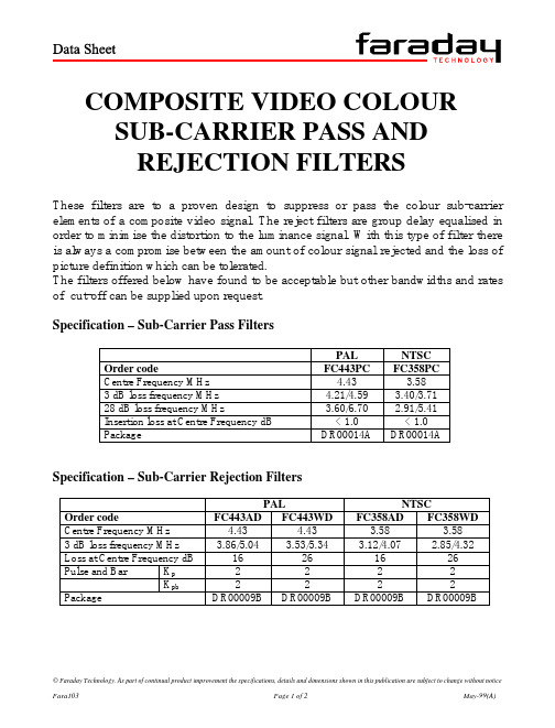
COMPOSITE VIDEO COLOUR SUB-CARRIER PASS AND REJECTION FILTERS
These filters are to a proven design to suppress or pass the colour sub-carrier elements of a composite video signal. The reject filters are group delay equalised in order to minimise the distortion to the luminance signal. With this type of filter there is always a compromise between the amount of colour signal rejected and the loss of picture definition which can be tolerated. The filters offered below have found to be acceptable but other bandwidths and rates of cut-off can be supplied upon request. Specification – Sub-Carrier Pass Filters
csk单向轴承规格型号

20CSK..2RSCSKType CSK is a sprag type freewheel integrated into a 62 series ball bearing (except sizes 8 and 40). It is bearing supported, delivered grease lubricated and protectedagainst dust of more than 0,3 mm. The use of additional “nylos” type seals is recommended especially when the working temperature exceeds 50°C. Oil bath lubrication is also possible.All the CSK versions are equipped with “formchromed” sprags. This process increases several times the overrunning life time. Torque transmission is ensured by a press fit assembly into a rigid outer housing with N6 tolerance, and onto a shaft with n6 tolerance. The initial bearing radial clearance is set at C5, and is reduced if using the press fit as specified.Please contact us when either the ambient or the operating temperature is not within the range +5°C to+60°C. CSK..2RS is 5 mm wider but is equiped with lip seals to be water splash resistant.STIEBER »COMBINED BEARING/FREEWHEEL »TYPE CSK, CSK..2RS»WWW.STIEBER.DE21CSKCSK..2RSCSK CSK..2RS1) T max = 2 × T KN» Refer to Selection page 10 to 13*) One Z seal on the bearing side only. Looking from this side, the outer race runs free in the counterclockwise direction **) Only one RS seal on the ball bearing side looking from this side, the outer race runs free in the counterclock-wise direction» Refer to mounting and maintenance instructionspage 16 to 19NOTESMOUNTING EXAMPLES。
SC1105CS.TR中文资料
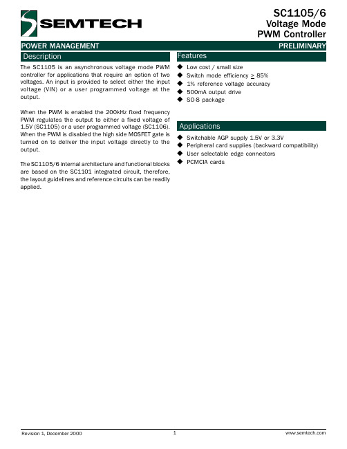
POWER MANAGEMENTSC1105/6Voltage ModePWM ControllerPRELIMINARY FeaturesApplicationsDescriptionThe SC1105 is an asynchronous voltage mode PWM controller for applications that require an option of two voltages. An input is provided to select either the input voltage (VIN) or a user programmed voltage at the output.When the PWM is enabled the 200kHz fixed frequency PWM regulates the output to either a fixed voltage of 1.5V (SC1105) or a user programmed voltage (SC1106). When the PWM is disabled the high side MOSFET gate is turned on to deliver the input voltage directly to the output.The SC1105/6 internal architecture and functional blocks are based on the SC1101 integrated circuit, therefore, the layout guidelines and reference circuits can be readily applied.u Low cost / small sizeu Switch mode efficiency > 85%u1% reference voltage accuracyu500mA output driveu SO-8 packageu Switchable AGP supply 1.5V or 3.3Vu Peripheral card supplies (backward compatibility) u User selectable edge connectorsu PCMCIA cardsPOWER MANAGEMENT PRELIMINARYElectrical CharacteristicsAbsolute Maximum Ratingsr e t e m a r a P l o b m y S m u m i x a M s t i n U e g a t l o V t u p n I V C C D N G o t 7+o t 3.0-V l a i t n e r e f f i D d n u o r G P D N G D N G o t +1V e g a t l o V t u p n I t s o o B DN G o t T S B 51+o t 3.0-V e r u t a r e p m e T g n i t a r e p O T A 07+o t 0C °eg n a R e r u t a r e p m e T e g a r o t S T G T S 521+o t 54-C °.c e S 01)g n i r e d l o S (e r u t a r e p m e T d a e L T L 003C °t n e i b m A o t n o i t c n u J ,e c n a t s i s e R l a m r e h T q A J 561W /C °e s a C o t n o i t c n u J ,e c n a t s i s e R l a m r e h T q C J 04W /C °)l e d o M y d o B n a m u H (g n i t a R D S E DS E 2Vk V CC = 4.75V to 5.25V; GND = P GND = 0V; V O = 1.5V; T A = 25°C; BST = 12V; 2A; V IN = 3.3V + 5%.Per test circuit, unless otherwise specified.r e t e m a r a P l o b m y S s n o i t i d n o C n i M p y T x a M s t i n U ec n e r e f e R V FE R 832.1052.1362.1Vpm e T r e v O 522.1052.1572.1t n e r r u C s a i B E S N E S O V I B 6011C S 0.20.8A µt n e r r u C t n e c s e i u Q I Q V o t n i t n e r r u C C C n i p 0.50.8A m d a o L n o i t a l u g e R G E R D A O L I O A8o t A 1=5.00.1%e n i L n o i t a l u g e R G E R E N I L 1.0%y c n e u q e r F r o t a l l i c s O C S O 081002022z H k e l c y C y t u D x a M .c .d 0959%tn e r r u C e c r u o S /k n i S H D I OV T S B V 5.4=H D -V (H D V -D N G P )V 2=005AmPOWER MANAGEMENT PRELIMINARY Test CircuitPOWER MANAGEMENT PRELIMINARYBlock DiagramPin ConfigurationOrdering InformationPin DescriptionsTop View(8 Lead Plastic SOIC)ec i v e D )1(e g a k c a P T (e g n a R p m e T J )R T .S C 5011C S 8-O S C °521o t °0RT .S C 6011C S 8-O S C°521o t °0Note:(1) Only available in tape and reel packaging. A reel contains 2500 devices.#n i P em a N n i P no i t c n u F n i P 1V C C .e g a t l o v y l p p u s e c i v e D 2C N .n o i t c e n n o c o N 3#T E D E P Y T .e l b i t a p m o c L T T -t u p n i l e v e l c i g o L .V 5.1=o L ;V 3.3=i H ,t c e l e s e g a t l o v t u p t u O 4D N G P .d n u o r g r e w o p e c i v e D 5H D .t u p t u o r e v i r d e d i s h g i H 6T S B .r e v i r d e d i s h g i h r o f y l p p u S V 217E S N E S O V .n i a h c k c a b d e e f l a n r e t n i f o d n e p o T 8DN G .d n u o r g l a n g i s l l a m SPOWER MANAGEMENT PRELIMINARY Typical CharacteristicsPOWER MANAGEMENT PRELIMINARYSemtech CorporationPower Management Products Division 652 Mitchell Rd., Newbury Park, CA 91320Phone: (805)498-2111 FAX (805)498-3804Outline DrawingContact InformationLand Pattern - SO-8。
山特c1ks参数

山特c1ks参数
山特城堡系列在线式UPS,包括容量1KVA至20KVA的一系列的UPS产品,其基本参数如下:
UPS类型:在线式。
额定功率:1KVA。
输入电压范围:V。
输入频率范围:软件可调:40--60 Hz。
输出电压范围:220(1±2%)V。
输出频率范围:与输入同步(市电模式),当市电频率超出(46~54)Hz 范围时,输出频率为50×(1±%)Hz。
输出电压波形:正弦波。
过载能力:%维持30秒钟后输出转为旁路,150%以上维持300ms。
外观尺寸:400×145×220mm。
产品重量:7kg。
其它性能:外接电池标称电压36VDC,操作温度0℃~40℃,操作湿度20%~90%。
随机附件:外接电池连接线 x1,用户手册(光盘) x1,简易安装操作指南1 张,长效型 x1,环保信息卡 x1。
如需更多山特UPS产品信息,建议访问山特官方网站进行查询或咨询相关人员。
变压器互感器产品推介讲稿1

互感器
产品介绍
传感器
北京新创四方电子有限公司
1992年中国第一款全封闭式变压器在我公司诞生,填补 了这类变压器国内空白,开创了中国变压器市场的新天 地,至今已为国内外广大客户朋友提供了数以亿计的各 类变压器/互感器,以设计先进,真材实料,品质可靠, 赢得了广大客户朋友的信赖。 今天,“BingZi 兵字”已然成为业界知名品牌,业内标杆。
北京新创四方电子有限公司
R、SR型系列电源变压器产品介绍
对比 系列 R系列 SR系列 功率范围 8-7.5KVA 60-15KVA 结构种类 19种结构 15种结构 型号 上千种型号 上百种型号
• 更可根据客户不同要求定做
北京新创四方电子有限公司
经济型系列变压器
• CD型电源变压器 • EI型电源变压器 • 其他
银天使系列、蓝精灵系列性能对比
类型 对比 环境温度 绝缘耐热等级 电压波动范围 功率范围 其他
S、SL
-25℃~+70℃ F级(155 ℃) 输入电压±25% 0.25-40VA 内置温保,更安全
T、TL
-10℃~+40℃ B级(130 ℃) 输入电压±10% 0.5-20VA 体积小,性价比好
• 注:SL,TL为扁平式变压器,表示这类产品比功率 代码后面没有“L”字符的同功率全封闭印刷线路板焊接式电源变压器
蓝精灵 T、TL系列特点: • 全封闭印刷线路板直接焊接安装,使用方便、外 形美观 • 结构紧凑、坚固、抗振、防潮、阻燃、抗电强度 高 • 体积小、功率密度大;经济适用,价格低 • 有22个系列,379种标准型号, 上千种非标型号 • 可根据用户要求定制
北京新创四方电子有限公司
典型应用电路
凯克斯设备说明书中文版(仅作参考)
名义直径: 总长度:
3.18 mm (0.125″) 6200mm(244″)
KX170 机械说明书(B)
7/21
Kayex 机密
KX170 设备说明书
2.5 热屏提升
在设备的炉盖上设计有两点式的热屏提升机构。热屏的位置可以通过在 手动模式下的触摸屏来控制,同样也可以通过自动模式下的计算机控 制。自动模式下通过斜率表来控制移动。两个热屏提升口在炉盖上相隔 180 度分布。
极限真空压力: 泄漏率(压力上升速率):
一般 25mtorr(该值是由真空泵和真空系 统决定) 50mtorr/hr
2.6.5. 氧化物控制系统
主真空系统在两个主真空接口的下游处都配置了一个空气注射阀用来 控制氧化物,通过计算机可以同时控制两个阀的开启,每个注射口的流 量稳定在大约或少于 5 升/分钟。
305mm(12″) 2800mm(110″)
KX170 机械说明书(B)
4/21
Kayex 机密
KX170 设备说明书
2.1.7 副室延长室
副室延长室是位于副炉室上部的一个圆筒形腔体。
延长室高度: 延长室内径:
508mm(20″) 191mm(7.5″)
2.1.8 水平调整器
水平调整器是封闭副室延长室上部并用来支撑籽晶提升的装配组件。通 过调整上法兰可以使籽晶旋转轴铅直垂直。水平调整器有两个氩气接入 口,一个熔体温度计接口,一个辅助真空接口。
隔离阀内径:
305mm(12″)
2.1.6 副炉室(接收室)
副炉室是位于隔离阀上的一圆筒形腔体。副炉室上设有便于操作者观察 的观察窗口(1)和籽晶位置监测口(2)。在副炉室上方的水平调整器 设有氩气进气接口(2),熔体测温计(1),一个辅助真空系统抽真空接 口。在副炉室上端还有一个清扫口。
E27是基于SI4432芯片的433MHz无线模块,小体积贴片型,发射功率高、接受灵敏度高、谐波小
SI4432无线模块E27系列本说明书可能会随着产品的不断改进有所更改,请以最新版的说明书为准成都亿佰特电子科技有限公司保留对本说明中所有内容的最终解释权及修改权版本修订日期修订说明维护人1.00 2017/12/05 初始版本huaa1.10 2018/01/30 型号名称变更huaa产品概述E27系列产品是成都亿佰特公司设计生产的一款433MHz射频模块,小体积贴片型(引脚间距1.27mm),最大功率20dBm。
模块自带高性能,弹簧天线,具有极好的阻抗匹配,具有发射功率高,接受灵敏度高,发射电流小,谐波小等特点。
E27系列产品采用Silicon Labs公司的SI4432射频芯片,芯片内置天线多样化和支持跳频,具有优越的抗干扰性能;同时,其内部还具有额外的功能,如:自动唤醒定时器,低电池电量检测器,64 字节发射/接收,自动数据包处理,集成温度传感器,模拟数字转化器,上电复位等等。
E27系列产品为硬件平台,出厂无程序,用户需要进行二次开发。
产品型号载波频率发射功率参考距离(PCB/IPX) 封装形式天线形式E27 (433M20S) 433M 20dBm 1600m 贴片邮票孔目录产品概述 (1)1. 技术参数 (3)1.1. E27(433M20S) (3)1.2. 参数说明 (3)2. 机械特性 (4)2.1 E27(433M20S) (4)2.1.1 尺寸图 (4)2.1.2 引脚定义 (4)3. 推荐连线图 (5)4. 生产指导 (5)2.2 回流焊温度 (5)2.3 回流焊曲线图 (6)5. 常见问题 (6)5.1. 通信距离很近 (6)5.2. 模块易损坏 (7)6. 重要声明 (7)7. 关于我们 (7)1.技术参数产品型号核心IC 尺寸模块净重工作温度工作湿度储存温度E27 (433M20S) SI4432 16 * 16 mm 0.7±0.1g -40 ~ 85℃10% ~ 90% -40 ~ 125°C1.1.E27 (433M20S)参数类别Min Typ Max 单位发射电流78 83 91 mA接收电流14.7 18.5 20.0 mA关断电流0.4 0.5 0.6 μA发射功率19 20 21 dBm 接收灵敏度-119 -121 -123 dBm 推荐工作频段425 433 525 MHz 供电电压 1.8 3.3 3.6 V通信电平 1.8 3.3 3.6 V1.2.参数说明●在针对模块设计供电电路时,往往推荐保留30%以上余量,有整机利于长期稳定地工作;●发射瞬间需求的电流较大但是往往因为发射时间极短,消耗的总能量可能更小;●当客户使用外置天线时,天线与模块在不同频点上的阻抗匹配程度不同会不同程度地影响发射电流的大小;●射频芯片处于纯粹接收状态时消耗的电流称为接收电流,部分带有通信协议的射频芯片或者开发者已经加载部分自行开发的协议于整机之上,这样可能会导致测试的接收电流偏大;●处于接纯粹收状态的电流往往都是mA级的,µA级的“接收电流”需要开发者通过软件进行处理;●当前灵敏度均为在空中速率为1kbps下测试;●关断电流往往远远小于整机电源部分的在空载时所消耗的电流,不必过分苛求;●由于物料本身具有一定误差,单个LRC元件具有±0.1%的误差,但犹豫在整个射频回路中使用了多个LRC元件,会存在误差累积的情况,致使不同模块的发射电流与接收电流存在差异;●降低发射功率可以一定程度上降低功耗,但由于诸多原因降低发射功率发射会降低内部PA的效率。
- 1、下载文档前请自行甄别文档内容的完整性,平台不提供额外的编辑、内容补充、找答案等附加服务。
- 2、"仅部分预览"的文档,不可在线预览部分如存在完整性等问题,可反馈申请退款(可完整预览的文档不适用该条件!)。
- 3、如文档侵犯您的权益,请联系客服反馈,我们会尽快为您处理(人工客服工作时间:9:00-18:30)。
PRELIMINARY - September 11, 2000TEL:805-498-2111 FAX:805-498-3804 WEB:
DESCRIPTION
The SC4431 is a four terminal device for regulating an isolated power supply with very low output voltage.
It is intended to be used as a replacement for three ter-minal shunt regulators such as SC431L where the out-put voltage is too low for them to function in conjunc-tion with an opto-isolator. It achieves this by having seperate supply and output pins, allowing the output to sink current at voltages as low as 0.2V, while the sup-ply pin still has sufficient voltage for the device to func-tion. In this way, allowing for a 1.6V drop through an opto-isolator diode, regulation down to 1.8V out can be achieved.
The SC4431 shunt regulator is available with three ini-tial reference voltage accuracies (0.5%, 1.0% and
2.0%) in the space saving 5-lead SOT-23 package. The three voltage tolerances allow the designer the opportunity to select the proper cost/tolerance for their application.FEATURES
•=Trimmed bandgap design - initial accuracies to + 0.5%
•=40mA drive capability
•=Wide supply voltage range - 1.5V to 15V
•=Low supply current - typically 110µA
•=Full industrial temperature range
APPLICATIONS
•=Opto driver for very low output voltage isolated power supplies
ORDERING INFORMATION
Part Number(1)(2)Package
SC4431CSK-X.TR SOT-23-5 Notes:
(1) Where “-X” denotes initial reference voltage toler-ance. Available options are ±0.5% (-.5), ±1% (-1) and ±2% (-2).
(2) Only available in tape and reel packaging. A reel contains 3000 devices.
TYPICAL APPLICATION CIRCUIT
PRELIMINARY - September 11, 2000
ABSOLUTE MAXIMUM RATINGS
Parameter
Symbol Maximum Units Input Supply Voltage V CC -0.5 to +16V Output Voltage V OUT -0.5 to V CC V Reference Voltage V REF -0.5 to +4
V Continuous Output Current I OUT 40mA Reference Input Current
I REF 5mA Operating Ambient Temperature Range T A -40 to +85°C Operating Junction Temperature Range T J -40 to +150°C Storage Temperature Range
T STG -65 to +150
°C Thermal Impedance Junction to Ambient θJA 256°C/W Thermal Impedance Junction to Case θJC 81°C/W Power Dissipation at T A = 25°C
P D 475mW Lead Temperature (Soldering) 10 seconds T LEAD 300°C ESD Rating (Human Body Model)
ESD
2
kV
ELECTRICAL CHARACTERISTICS
Unless specified, T A = 25°C, V CC = 2V, I OUT = 2mA. Values in bold apply over full operating temperature range.
PRELIMINARY - September 11, 2000
ELECTRICAL CHARACTERISTICS (Cont.)
Unless specified, T A = 25°C, V CC = 2V, I OUT = 2mA. Values in bold apply over full operating temperature range.
Parameter Symbol Test Conditions MIN TYP MAX Units REF (Cont.)
Reference Input Current
I REF
0.1mA ≤ I OUT ≤ 10mA
0.3
0.5µA
1.0
OUT
Saturation Voltage
V OUT(SAT)
I OUT = 5mA, I CC = 500µA 5075mV
100V REF = 1.261V, I OUT = 40mA
275300mV 400Off State Output Current
I OUT(OFF)
V REF = 1.187V, V OUT = 2V
0.5
1µA 10
PRELIMINARY - September 11, 2000
BLOCK DIAGRAM
PIN CONFIGURATION
PIN DESCRIPTION
Pin Pin Name Pin Function
1VCC This is the input supply pin for the IC.
2GND Logic and power ground.
3NC No connection.
4REF This is connected to the non-inverting input of the error amplifier. 5OUT This is the output pin of the device, essentially an open collector.
LAND PATTERN - SOT-23-5
ECN 00-1315。