3296W503中文资料
BY329X-1500S,127;BY329X-1500,127;中文规格书,Datasheet资料
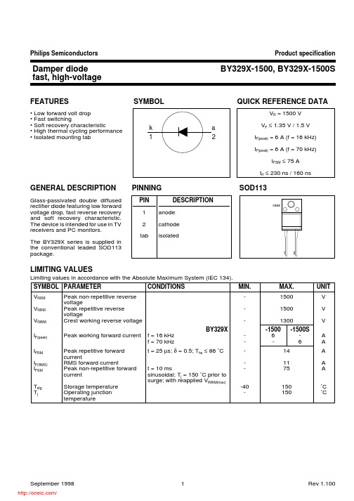
Philips Semiconductors Product specificationDamper diode BY329X-1500, BY329X-1500Sfast, high-voltageFEATURESSYMBOL QUICK REFERENCE DATA• Low forward volt drop • Fast switching• Soft recovery characteristic• High thermal cycling performance • Isolated mounting tabGENERAL DESCRIPTIONPINNINGSOD113Glass-passivated double diffused PIN DESCRIPTION rectifier diode featuring low forward voltage drop,fast reverse recovery 1anode and soft recovery characteristic.The device is intended for use in TV 2cathode receivers and PC monitors.tabisolatedThe BY329X series is supplied in the conventional leaded SOD113package.LIMITING VALUESLimiting values in accordance with the Absolute Maximum System (IEC 134).SYMBOL PARAMETER CONDITIONSMIN.MAX.UNIT V RSM Peak non-repetitive reverse -1500V voltageV RRM Peak repetitive reverse -1500V voltageV RWM Crest working reverse voltage -1300V BY329X-1500-1500S I F(peak)Peak working forward current f = 16 kHz -6-A f = 70 kHz--6A I FRM Peak repetitive forward t = 25 µs; δ = 0.5; T hs ≤ 86 ˚C -14A currentI F(RMS)RMS forward current-11A I FSM Peak non-repetitive forward t = 10 ms-75A currentsinusoidal; T j = 150 ˚C prior to surge; with reapplied V RWM(max)T stg Storage temperature -40150˚C T jOperating junction -150˚Ctemperature12casePhilips Semiconductors Product specification Damper diode BY329X-1500, BY329X-1500S fast, high-voltageISOLATION LIMITING VALUE & CHARACTERISTICThs= 25 ˚C unless otherwise specifiedSYMBOL PARAMETER CONDITIONS MIN.TYP.MAX.UNITVisol R.M.S. isolation voltage from f = 50-60 Hz; sinusoidal-2500V both terminals to external waveform;heatsink R.H. ≤ 65% ; clean and dustfreeCisol Capacitance from both terminals f = 1 MHz-10-pF to external heatsinkTHERMAL RESISTANCESSYMBOL PARAMETER CONDITIONS MIN.TYP.MAX.UNITRth j-hs Thermal resistance junction to with heatsink compound-- 4.8K/W heatsink without heatsink compound-- 5.9K/WRth j-a Thermal resistance junction to in free air.-55-K/W ambientSTATIC CHARACTERISTICSTj= 25 ˚C unless otherwise statedSYMBOL PARAMETER CONDITIONS TYP.MAX.UNITBY329X-15001500S15001500SVF Forward voltage IF= 6.5 A 1.1 1.3 1.45 1.6VIF= 6.5 A; Tj= 125 ˚C 1.05 1.2 1.35 1.5VI R Reverse current VR= 1300 V-250-250µAVR= 1300 V; Tj= 125 ˚C-1-1mADYNAMIC CHARACTERISTICSTj= 25 ˚C unless otherwise statedSYMBOL PARAMETER CONDITIONS TYP.MAX.UNITBY329X15001500S15001500St rr Reverse recovery time IF= 1 A; VR≥ 30 V;0.180.130.230.16µsdIF/dt = 50A/µsQs Reverse recovery charge IF= 2 A; -dIF/dt = 20 A/µs 1.60.7 2.00.95µCVfr Peak forward recovery voltage IF= 6.5A; dIF/dt = 50A/µs1*******Vt fr Forward recovery time IF= 6.5A; dIF/dt = 50A/µs210220300320nsPhilips Semiconductors Product specificationDamper diode BY329X-1500, BY329X-1500Sfast, high-voltagePhilips Semiconductors Product specificationDamper diode BY329X-1500, BY329X-1500Sfast, high-voltagePhilips Semiconductors Product specificationDamper diode BY329X-1500, BY329X-1500Sfast, high-voltageMECHANICAL DATA1. Refer to mounting instructions for F-pack envelopes.2. Epoxy meets UL94 V0 at 1/8".Philips Semiconductors Product specification Damper diode BY329X-1500, BY329X-1500S fast, high-voltageDEFINITIONSData sheet statusObjective specification This data sheet contains target or goal specifications for product development. Preliminary specification This data sheet contains preliminary data; supplementary data may be published later. Product specification This data sheet contains final product specifications.Limiting valuesLimiting values are given in accordance with the Absolute Maximum Rating System (IEC 134). Stress above one or more of the limiting values may cause permanent damage to the device. These are stress ratings only and operation of the device at these or at any other conditions above those given in the Characteristics sections ofthis specification is not implied. Exposure to limiting values for extended periods may affect device reliability. Application informationWhere application information is given, it is advisory and does not form part of the specification.© Philips Electronics N.V. 1998All rights are reserved. Reproduction in whole or in part is prohibited without the prior written consent of the copyright owner.The information presented in this document does not form part of any quotation or contract, it is believed to be accurate and reliable and may be changed without notice. No liability will be accepted by the publisher for any consequence of its use. Publication thereof does not convey nor imply any license under patent or other industrial or intellectual property rights.LIFE SUPPORT APPLICATIONSThese products are not designed for use in life support appliances, devices or systems where malfunction of these products can be reasonably expected to result in personal injury. Philips customers using or selling these products for use in such applications do so at their own risk and agree to fully indemnify Philips for any damages resulting from such improper use or sale.分销商库存信息:NXPBY329X-1500S,127BY329X-1500,127。
Protek 3201_3290N 中文说明书_东方嘉仪

误动作时
U
U
虽然此仪器的电源可以开机,如有误动作(不正常工作或死机现象)时,请按照下述步骤安 全使用。
1) Protek 3201N/3290N接上电源(电源适配器AC Adapter)。 2) 按Reset 键。 (Reset 键在 Battery 装入口的底面) 3) 不正常工作时, 另外有一种方法是 通过系统菜单(Menu)的测试(TEST)组上选择
PC电脑连接(Connection for PC)……………………………………………………………64
自动电源Auto Power……………………………………………………………………………65
偏置Offset……………………………………………………………………………………66
菜单(Menu)…………………………………………………………………………………67
电 话 :(青 岛 )0532-86069117 (南京)025-52405707 (天津)022-60501825
9
3201N/3290N 用户手册
仪器仪表销售 注册品牌
存储 /读出Save/Load ………………………………………………………………………54
频率计数器(Frequency Counter)………………………………………………………58
RESET 键即可。
电池 (Battery)
U
此仪器使用Ni-MH Rechargeable Battery(镍-氢充电电池;以下称Ni-MH充电电池) 6个,可 以充电后使用。
1) Ni-MH充电电池为消耗品,随着使用时间的增加,Ni-MH充电电池的寿命会缩短。 2) Ni-MH 充电电池的实际使用时间,缩短为刚刚购买时的实际使用时间一半时请更换
5056中文资料
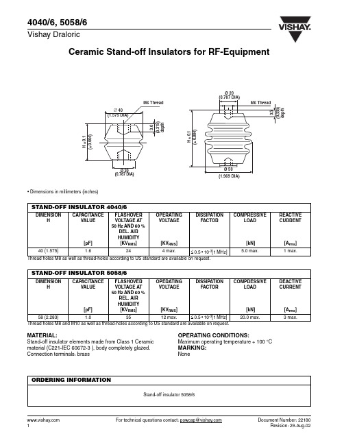
Ceramic Stand-off Insulators for RF-Equipment For technical questions contact: powcap@Document Number: 221801Revision: 29-Aug-024040/6, 5058/6Vishay Draloric• Dimensions in millimeters (inches)Thread holes M8 as well as thread-holes according to US standard are available on request.Thread holes M8 and M10 as well as thread-holes according to US standard are available on request.STAND-OFF INSULATOR 4040/6DIMENSIONHCAPACITANCEVALUE[pF]FLASHOVER VOLTAGE AT 50 Hz AND 60 %REL. AIR HUMIDITY [KV RMS ]OPERATING VOLTAGE[KV RMS ] DISSIPATION FACTORCOMPRESSIVELOAD[kN] REACTIVE CURRENT[A rms ] 40 (1.575)1.6244 max.≤ 0.5 • 10-3[1 MHz]5.0 max.1 max.STAND-OFF INSULATOR 5058/6DIMENSIONHCAPACITANCEVALUE[pF]FLASHOVER VOLTAGE AT 50 Hz AND 60 %REL. AIR HUMIDITY [KV RMS ]OPERATING VOLTAGE[KV RMS ] DISSIPATION FACTORCOMPRESSIVELOAD[kN] REACTIVE CURRENT[A rms ] 58 (2.283)1.03512 max.≤ 0.5 • 10-3[1 MHz]20.0 max.3 max.MATERIAL:Stand-off insulator elements made from Class 1 Ceramic material (C221-IEC 60672-3 ), body completely glazed. Connection terminals: brassOPERATING CONDITIONS:Maximum operating temperature + 100 °CMARKING:NoneORDERING INFORMATIONStand-off insulator 5058/6元器件交易网Document Number: 91000Revision: 18-Jul-081DisclaimerLegal Disclaimer NoticeVishayAll product specifications and data are subject to change without notice.Vishay Intertechnology, Inc., its affiliates, agents, and employees, and all persons acting on its or their behalf (collectively, “Vishay”), disclaim any and all liability for any errors, inaccuracies or incompleteness contained herein or in any other disclosure relating to any product.Vishay disclaims any and all liability arising out of the use or application of any product described herein or of any information provided herein to the maximum extent permitted by law. The product specifications do not expand or otherwise modify Vishay’s terms and conditions of purchase, including but not limited to the warranty expressed therein, which apply to these products.No license, express or implied, by estoppel or otherwise, to any intellectual property rights is granted by this document or by any conduct of Vishay.The products shown herein are not designed for use in medical, life-saving, or life-sustaining applications unless otherwise expressly indicated. Customers using or selling Vishay products not expressly indicated for use in such applications do so entirely at their own risk and agree to fully indemnify Vishay for any damages arising or resulting from such use or sale. Please contact authorized Vishay personnel to obtain written terms and conditions regarding products designed for such applications.Product names and markings noted herein may be trademarks of their respective owners.元器件交易网。
20欧3296w电位器最大阻值

20欧3296w电位器最大阻值电位器是一种用来调节电路中电阻值的元件,是电子电路中常见的一种被广泛应用的元器件。
在电子设备中,电位器通常用来调节电压、电流和功率等参数,以实现对电路的控制和调节。
电位器也被称为“电位调节器”、“电阻器”或“可变电阻器”。
在本文中,我将为您详细介绍20欧3296w电位器的最大阻值。
20欧3296w电位器是一种带有旋钮的电阻器,其最大阻值为20欧。
它通常由一个转动的电阻元件和一个旋钮组成。
通过旋转电位器的旋钮,可以改变其电阻值,从而调节电路中的电流或电压。
一般情况下,电位器在电子电路中起到调节和控制电流或电压的作用,是一种非常实用的元件。
电位器的最大阻值是指在最高位置时,电位器的电阻达到的最大值。
在20欧3296w电位器中,其最大阻值为20欧。
换句话说,当旋钮旋转到最高位置时,电位器的电阻将达到最大值20欧姆。
这也意味着在使用过程中,电位器的阻值可以从0到20欧姆之间连续调节。
对于20欧3296w电位器的最大阻值,我们可以从以下几个方面进行详细分析和介绍:1.电位器的结构和工作原理:20欧3296w电位器通常由一个旋转的电阻元件和一个旋钮组成。
电阻元件是一个圆筒形的陶瓷基座,上面有导电材料涂层,并绕成螺旋形。
通过旋转电位器的旋钮,可以改变电阻元件上的导电材料的长度,从而改变电位器的电阻值。
2.电位器的调节范围:在20欧3296w电位器中,其最大阻值为20欧。
这意味着在使用过程中,电位器的阻值可以从0到20欧姆之间连续调节。
通过旋转电位器的旋钮,可以选择不同的阻值来调节电路中的电流或电压。
3.电位器的应用领域:20欧3296w电位器广泛应用于各种类型的电子设备和电路中。
例如,它可以用于调节音量、亮度和对比度等参数的控制,也可以用于电源电压的调节、温度传感器的校准等。
另外,电位器还可以用于电流限制、信号放大和滤波等应用。
4.电位器的注意事项:在使用20欧3296w电位器时,需要注意一些事项。
AD404M326VQA-5中文资料

ASCEND Semiconductor 4Mx4 EDO Data sheetDescriptionThe device CMOS Dynamic RAM organized as 4,194,304 words x 4 bits with extended data out access mode. It is fabricated with an advanced submicron CMOS technology and designed to operate from a single 3.3V oniy power supply. Low voltage operation is more suitable to be used on battery backup, portable elec-tronic application. lt is packaged in JEDEC standard 26/24-pin plastic SOJ or TSOP(II).Features• Single 3.3V(%) only power supply • High speed t RAC acess time: 50/60ns • Low power dissipation- Active mode : 432/396 mW (Mas) - Standby mode: 0.54 mW (Mas)• Extended - data - out(EDO) page mode access • I/O level: CMOS level (Vcc = 3.3V)• 2048 refresh cycle in 32 ms(Std.) or 128 ms(S-version)• 4 refresh modesh: - RAS only refresh- CAS - before - RAS refresh - Hidden refresh - Self-refresh(S-version)10±Pin Name FunctionA0-A10Address inputs- Row address - Column address - Refresh address DQ1~DQ4Data-in / data-out RAS Row address strobe CAS Column address strobe WE Write enable OE Output enable Vcc Power (+ 3.3V)VssGroundVCC 1DQ12DQ23DQ34DQ45VCC6891011 NC 12 WE 13A0 A117 A218 A319VSS RAS CAS OE A8A7A6A5A4VSSAD404M42VSPin Description Pin Configuration21222324 2526151416 A1026/24-PIN 300mil Plastic SOJA9VCC 1DQ12DQ23DQ34DQ45VCC6891011 NC 12 WE 13A0 A117 A218 A319VSS RAS CAS OE A8A7 A6A5 A4VSSAD404M42VT212223242526151416 A1026/24-PIN 300mil Plastic TSOP (ll)A9A0-A10A0-A10A0-A10WECASNO. 2 CLOCK GENERATORCOLUMN ADDRESS BUFFERS (11)REFRESH CONTROLLERREFRESH COUNTERBUFFERS (11)ADDRESS ROW NO. 1 CLOCK GENERATORA0RASA1A2A3A4A5A6A7A8CONTROLLOGICDATA-IN BUFFERDATA-OUT BUFFEROEDQ1.DQ4.COLUMN DECODER2048SENSE AMPLIFIERSI/O GATING2048x42048x2048x4MEMORY ARRAY2048R O W D E C O D E RVcc VssBlock DiagramA9A10TRUTH TABLENotes: 1. EARLY WRITE only.FUNCTIONRASCAS WE OE ADDRESSESDQ SNotesROW COL STANDBY H X X X X High-Z READL L H L ROW COL Data-Out WRITE: (EARLY WRITE )L L L X ROW COL Data-lnREAD WRITE L L ROW COL Data-Out,Data-ln EDO-PAGE-MODE READ1st Cycle L H L ROW COL Data-Out 2nd CycleL H L n/a COL Data-Out EDO-PAGE MODE WRITE1st CycleL L X ROW COL Data-In 2nd Cycle L L Xn/a COL Data-InEDO-PAGE-MODEREAD-WRITE 1st Cycle L ROW COL Data-Out, Data-In 2nd Cycle L n/a COL Data-Out, Data-In HIDDEN REFRESHREAD L H L ROW COL Data-Out WRITEL L X ROW COL Data-In 1RAS-ONLY REFRESH L H X X ROW n/a High-Z CBR REFRESHLHXXXHigh-ZH X →H L →L H →H L →H L →H L →H L →H L →H L →L H →H L →H L →L H→L H L →→L H L→→H L→Absolute Maximum RatingsRecommended DC Operating ConditionsCapacitanceTa = 25°C, V CC = 3.3V%, f = 1MHz Note: 1. Capacitance measured with effective capacitance measuring method. 2. RAS, CAS = V IH to disable Dout.ParameterSymbol Value Unit Voltage on any pin relative to Vss V T -0.5 to + 4.6V Supply voltage relative to Vss V CC -0.5 to + 4.6V Short circuit output current I OUT 50mA Power dissipation P D 1.0WOperating temperature T OPT 0 to + 70°C Storage temperatureT STG-55 to + 125°CParameter/Condition Symbol3.3 Volt VersionUnitMinTyp MaxSupply VoltageV CC 3.0 3.33.6V Input High Voltage, all inputs V IH 2.0-V CC + 0.3V Input Low Voltage, all inputsV IL-0.3-0.8VParameterSymbol Typ Max Unit Note Input capacitance (Address)C I1 -5pF 1Input capacitance (RAS, CAS, OE, WE)C I2-7pF 1Output capacitance(Data-in, Data-out)C I/O-7pF1, 210±DC Characteristics :(T a = 0 to 70°C, V CC = + 3.3V%, V SS = 0V)Parameter Symbol Test Conditions AD404M42V Unit Notes-5-6Min Max Min MaxOperating current I CC1RAS cyclingCAS, cyclingt RC = min-120-110mA1, 2Standby Current LowpowerS-versionI CC2LVTTL interfaceRAS, CAS = V IHDout = High-Z-0.5-0.5mACMOS interfaceRAS, -0.2VDout = High-Z-0.15-0.15mAStandardpowerversionLVTTL interfaceRAS, CAS = V IHDout = High-Z-2-2mACMOS interfaceRAS,-0.2VDout = High-Z-0.5-0.5mARAS- only refresh current I CC3RAS cycling, CAS = V IHt RC = min-120-110mA1, 2 EDO page mode current I CC4t PC = min-90-80mA1, 3CAS- before- RAS refresh current I CC5t RC = minRAS, CAS cycling-120-110mA1, 2Self- refresh current (S-Version)I CC8 - 550 - 55010±CAS V CC≥CAS V CC≥t RASS100µs≥µADC Characteristics :(T a = 0 to 70°C , V CC = +3.3V %, V SS = 0V)Notes:1. I CC is specified as an average current. It depends on output loading condition and cycle rate when the device is selected. I CC max is specified at the output open condition.2. Address can be changed once or less while RAS = V IL .3. For I CC4, address can be changed once or less within one EDO page mode cycle time.Parameter Symbol Test Conditions AD404M42VUnitNotes-5-6Min MaxMin MaxInput leakage current I LI + 0.3V -55-55Output leakage current I LO + 0.3V Dout = Disable -55-55Output high Voltage V OH I OH = -2mA 2.4- 2.4-V Output low voltage V OLI OL = +2mA-0.4-0.4V10±0V Vin V CC ≤≤µA 0V Vout V CC ≤≤µAAC Characteristics(T a = 0 to + 70°C , V cc = 3.3V %, V ss = 0V) *1, *2, *3, *4Test conditions• Output load: one TTL Load and 100pF (V CC = 3.3V %)• Input timing reference levels:V IH = 2.0V, V IL = 0.8V (V CC = 3.3V %)• Output timing reference levels:V OH = 2.0V, V OL = 0.8V10±10±10±Read, Write, Read- Modify- Write and Refresh Cycles (Common Parameters)ParameterSymbol AD404M42V UnitNotes-5-6Min MaxMin MaxRandom read or write cycle time t RC 84-104-ns RAS precharge timet RP 30-40-ns CAS precharge time in normal mode t CPN 10-10-ns RAS pulse width t RAS 50100006010000ns 5CAS pulse width t CAS 8100001010000ns 6Row address setup time t ASR 0-0-ns Row address hold time t RAH 8-10-ns Column address setup time t ASC 0-0-ns 7Column address hold time t CAH 8-10-ns RAS to CAS delay timet RCD 12371445ns 8RAS to column address delay time t RAD 10251230ns 9Column address to RAS lead time t RAL 25-30-ns RAS hold time t RSH 8-10-ns CAS hold timet CSH 38-40-ns CAS to RAS precharge time t CRP 5-5-ns 10OE to Din delay time t OED 12-15-ns Transition time (rise and fall)t T 150150ns 11Refresh periodt REF -32-32ms Refresh period (S- Version)t REF -128-128ms CAS to output in Low- Z t CLZ 0-0-ns CAS delay time from Din t DZC 0-0-ns OE delay time from Dint DZO-0-nsRead CycleWrite Cycle Parameter SymbolAD404M42V Unit Notes-5-6Min Max Min MaxAccess time from RAS t RAC-50-60ns12 Access time from CAS t CAC-14-15ns13, 14 Access time from column address t AA-25-30ns14, 15 Access time from OE t OEA-12-15nsRead command setup time t RCS0-0-ns7 Read command hold time to CAS t RCH0-0-ns10, 16 Read command hold time to RAS t RRH0-0-ns16 Output buffer turn-off time t OFF012015ns17 Output buffer turn-off time from OE t OEZ012015ns17Parameter SymbolAD404M42V Unit Notes -5-6Min Max Min MaxWrite command setup time t WCS0-0-ns7, 18 Write command hold time t WCH8-10-nsWrite command pulse width t WP8-10-nsWrite command to RAS lead time t RWL13-15-nsWrite command to CAS lead time t CWL8-10-nsData-in setup time t DS0-0-ns19 Data-in hold time t DH8-10-ns19 WE to Data-in delay t WED10-10-nsRead- Modify- Write CycleRefresh Cycle Parameter SymbolAD404M42V Unit Notes-5-6Min Max Min MaxRead-modify- write cycle time t RWC108-133-nsRAS to WE delay time t RWD64-77-ns18 CAS to WE dealy time t CWD26-32-ns18 Column address to WE delay time t AWD39-47-ns18 OE hold time from WE t OEH8-10-nsParameter SymbolAD404M42VUnit Notes -5-6Min Max Min MaxCAS setup time (CBR refresh) t CSR5-5-nsCAS hold time (CBR refresh)t CHR8-10-ns10 RAS precharge to CAS hold time t RPC5-5-ns7 RAS pulse width (self refresh)t RASS100-100-RAS precharge time (self refresh)t RPS90-110-nsCAS hold time (CBR self refresh)t CHS-50--50-nsWE setup time t WSR0-0-nsWE hold time t WHR10-10-nsµsEDO Page Mode CycleEDO Page Mode Read Modify Write CycleParameterSymbol AD404M42VUnit Notes-5-6Min MaxMin MaxEDO page mode cycle timet PC 20-25-ns EDO page mode CAS precharge time t CP 10-10-ns EDO page mode RAS pulse width t RASP 5010560105ns 20Access time from CAS precharge t CPA -30-35ns 10, 14RAS hold time from CAS precharge t CPRH 30-35-ns OE high hold time from CAS high t OEHC 5-5-ns OE high pulse widtht OEP 10-10-ns Data output hold time after CAS low t COH 5-5-ns Output disable delay from WEt WHZ 310310ns WE pulse width for output disable whenCAS hight WPZ7-7-nsParameterSymbol AD404M42V Unit Notes -5-6Min MaxMin MaxEDO page mode read- modify- write cycle CAS precharge to WE delay timet CPW 45-55-ns 10EDO page mode read- modify- write cycle timet PRWC56-68-nsNotes :1. AC measurements assume t T = 2ns.2. An initial pause of 100 is required after power up, and it followed by a minimum of eightinitialization cycles (RAS - only refresh cycle or CAS - before - RAS refresh cycle). If the internal refresh counter is used, a minimun of eight CAS - before - RAS refresh cycles are required.3. In delayed write or read-modify-write cycles, OE must disable output buffer prior to applying data to the device.4. All the V CC and V SS pins shall be supplied with the same voltages.5. t RAS (min) = t RWD (min)+t RWL (min)+t T in read-modify-write cycle.6. t CAS (min) = t CWD (min)+t CWL (min)+t T in read-modify-write cycle.7. t ASC (min), t RCS (min), t WCS (min), and t RPC are determined by the falling edge of CAS .8. t RCD (max) is specified as a reference point only, and t RAC (max) can be met with the t RCD (max) limit.Otherwise, t RAC is controlled exclusively by t CAC if t RCD is greater than the specified t RCD (max) limit. 9. t RAD (max) is specified as a reference point only, and t RAC (max) can be met with the t RAD (max) limit.Otherwise, t RAC is controlled exclusively by t AA if t RAD is greater than the specified t RAD (max) limit. 10. t CRP , t CHR , t RCH , t CPA and t CPW are determined by the rising edge of CAS .11. V IH (min) and V IL (max) are reference levels for measuring timing or input signals. Therefore, transitiontime is measured between V IH and V IL .12. Assumes that t RCD tRCD (max) and t RAD t RAD (max). If t RCD or t RAD is greater than the maximum recommended value shown in this table, t RAC exceeds the value shown. 13. Assumes that (max) and (max).14. Access time is determined by the maximum of t AA , t CAC , t CPA . 15. Assumes that (max) and (max). 16. Either t RCH or t RRH must be satisfied for a read cycle.17. t OFF (max) and t OEZ (max) define the time at which the output achieves the open circuit condition (highimpedance). t OFF is determined by the later rising edge of RAS or CAS.18. t WCS , t RWD , t CWD , and t AWD are not restrictive operating parameters. They are included in the datasheet as electrical characteristics only. If (min), the cycle is an early write cycle and the data out will remain open circuit (high impedance) throughout the entire cycle. If (min),(min), (min) and (min), the cycle is a read-modify-write and the data output will contain data read from the selected cell. If neither of the above sets of conditions is satisfied, the condition of the data output (at access time) is indeterminate.19. These parameters are referenced to CAS separately in an early write cycle and to WE edge in adelayed write or a read-modify-write cycle.20. t RASP defines RAS pulse width in EDO page mode cycles.µs ≤≤t RCD t RCD ≥t RADt RAD ≤t RCD t RCD ≤t RAD t RAD ≥t WCS t WCS ≥t RWD t RWD ≥t CWDt CWD ≥t AWD t AWD ≥t CPW t CPW≥Timing Waveforms• Read Cyclet RC t RASt RPtCRPtCPNtRRHtRCHt OEZ t OFF tOEA tCACt AAtRACt CLZD OUTtRCS t ASR tRAH tASC tCAH tRAD t RALtCAStRSH tRCDt TtCSHRASCASADDRESSWEDQ1~DQ4Note : = don’t care OEt OFFRowColumn= Invalid Dout•Early Write CycletRC t RASt RPt WCHt DSt DHt WCS t RALtCAStRSH tRCDt TtCSHRASCASWEDQ1~DQ4tCRPtASRtRAH tASCtCAH ADDRESSColumnRowtCPND INtRADt RAL• Delayed Write CycletRC t RASt RPt RWL t RCSt CAStRSH tRCDt TtCSHRASCAStASR tRAH tCAHADDRESSColumnRow tASC D INDQ1~DQ4WEtCRPtCPNt DHt DSt OEHt OEDOEt DSOPENt WPt CWL• Read - Modify - Write CycletRWC t RASt RPtRWDt WPtRADtRWL tCAStCWL tRCDt TtCPNRASCASWEtCRP t ASRtRAHtASCtCAHADDRESS Column RowDQ1~DQ4t DHt DSOEtRCStAWD tCWD D INt OEDt OEHt OEZt OEA t CAC t RACt AADQ1~DQ4D OUTOPENtDZCtDZO• EDO Page Mode Read CycletRASPtCPRHt RCStCAStRSH tRCDt OEAtCSHRASCAStASRtRAHtCAHADDRESStCASWEtCRPt CPOEDQ1~DQ4OPENtOEPD OUT 1t PCt CPtCAStCPNtCRPtRADtCAHtASCt ASCtCAHt ASCt RAL Row Column 1t OEAt OEHCtRRH tRCHt RACt AAt AAt AA t CPA t CPA t OEZt OFFt OFFt CACt OEZt CAC t CACt COHD OUT NWE OE Column 2Column N Rowt RPD OUT 2• EDO Page Mode Early Write CycletRASPtRPt WCSt CAStRSH tRCDRASCAStASRtRAHtCAHADDRESStCASWEt CPDQ1~DQ4t PCt CPt CAStCPNtCRP tCAH tASCtASC tCAH tASC Row Column 1t DS WE Column 2Column Nt WCH t WCS t WCH t WCS t WCHt DH t DS t DH t DS t DHD IN 1D IN 2D IN Nt TtCSH• EDO Page Mode Read-Early-Write Cyclet RASPtCPRHt RCStCAStRSH tRCDt OEAtCSHRASCAStASRtRAHtCAHADDRESStCASWEtCRPt CPOEDQ1~DQ4OPENtWEDt PCt CPtCAStCPNtCRPtRADtRAHtASCt ASCtCAHt ASCt RAL Row Column 1tWCStRCHt RACt AAt AAt CPA t DHt WHZt CACt CACt COHWE OE Column 2Column N Rowt RPt CAL tWCHDataDoutput 2Data Input NDataDoutput 1t DStCSH• EDO Page Mode Read-Modify-Write Cyclet RASPt CPRHt RCStCASt WP RASCASt ASRtRAHtCAHADDRESSt CASWEtRCDCPDQ1~DQ4tPRWCt CPtCAStCRPtRADtCAHtASCt ASCtCAH tASC Row Column 1tRWLtRCSt OEDt DZOt CAC WE OEt RPt RAL D OUT 2D OUT ND OUT 1tTt Column NColumn 2Column 1tRWD tAWD tCWDtCWLtRCStCWDtAWD tCPW tCWL tCPW tAWD tCWDtCWL t OEDt OEDt OEHt OEHt OEHt CAC t CAC t OEA t AAt RACt OEZt OEAt AA t CPAt OEZt OEAt AA t CPAt OEZ t DSt DHt WP t DSt DHt WP t DSt DHOPENOPENOPEN D IN 1D IN ND IN 2DQ1~DQ4t DZCt DZOt DZCt DZCt DZO• Read Cycle with WE Controlled Disablet WPZt RCStCAStRCDt TtCSHRASCASt ASRtRAHtCAHADDRESSColumnRow tASCD DQ1~DQ4WEt OEZt DSt WHZOEt RCH t OEA t CACt AAt RACt CLZOUTtRADRASADDRESSt RC t CRPt ASRt RAHt Tt RPCROWt OFFCAS t RASt RPOPENt CRPDQ1~DQ4RASt CSRt WSRt RPt T t RPCt OFFCAS t RASt RPOPENt CRPDQ1~DQ4t RPCt CHRt RASt RPt RCt RCt CHRt CSRt WHRt WSRt WHRWECAS-Before-RAS Refresh CycleRASWEt RPCt OFFt CSRt CHSt WSRCASt RASS t RPSOPENDQ1~DQ4t WHRHigh lmpedance• Hidden Refresh Cyclet RPt RASRASt RCDt CRPADDRESSWEt CHRt CASt RSHt RAHt ASRt ASCt CAHt RAL ROW t RCHt OEZCASDQ1~DQ4t Tt RCSD t RASt RASt RPt RPt RC t RCt RCt RADt RRHt OFF t OFFt OEA t CACt AAt RACCOlumnOUTOE(READ)(REFRESH)(REFRESH)Ordering informationAD404M42VSA-5• AD• Ascend Memory Product • 40 • Device Type• 4M4 • Density and Organization • 2• Refresh Rate, 2: 2K Refresh • V• T: 5V, V: 3.3V• S • Package Type (S : SOJ, T : TSOP II)• A• Version• 5• Speed (5: 50 ns, 6: 60 ns)Part Number Access time PackageAD404M42VSA-5AD404M42VSA-6AD404M42VTA-5AD404M42VTA-650 ns 60 ns 50 ns 60 ns300mil 26/24-Pin Plastic SOJTSOP IIPackaging information • 300 mil, 26/24-Pin Plastic SOJ• 300 mil, 26/24-Pin TSOP II。
PMAC503M说明书1222
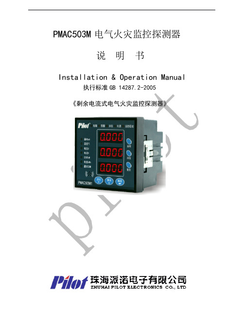
第 2 章 技术参数
2.1 PMAC503M1 参数说明
产品外貌
精度等级 漏电通道数 剩余电流动作值 ln( mA) 剩余电流预警值 lno(mA) 温度探测器报警范围 电压(V) 电流(A)
0.5 级 1路 100 ~1000 mA ,调节步长 1mA lno=1/2 ln 测量范围: 0~150 ℃,动作范围:55~140℃ ,±1℃ 三相四线,相电压 AC220V,精确至小数点后两位 四位显示,根据数值大小切换小数点位,精确至小 数点后三位
正面(96x96mm)
侧面 83.5mm
安装方式为面板式安装,方便操作观察,开孔尺寸为 90mm x 90mm。
第 1 章 产品介绍
1.1 产品设计说明 PMAC503 M 系列电气火灾监控探测器 (以下简称探测器 )主 要应用于低压 配电系统 (380/220VAC) 的漏电保护 和基本电参数 的测量。该系列探测器在实现漏电及温度等保护功能之外,还提 供对三相电压、电流、功率与电度等电量参数的监控。提供基于 RS485 或 C-MBUS 的 Modbus-RTU 协议的通讯, 也可与 Profibus 协议转换模块连接,实现 Profibus 通信,集中监控,系统管理。 PMAC503 M 系列电气火灾监控探测器 (剩余电流、温度探 测防火监控器)分为 PMAC503M1 ,PMAC503M4 ,PMAC503M8 等三种类型,分别提供一路,四路和八路的漏电监控通道,满足 了各种保护现场的需求。 该系列探测器采用先进的微电子技术,利用电子元件测量控 制电流大小及温度,以毫秒的速度检测线路的漏电情况及配电箱 内的温度,当被控制线路漏电,或监测点温度过高而发热时,该 系统会发出报警信号直至自动切断电源, 提供的消防联动功能, 可远程切断故障点的电源,将故障排除在起火之前,彻底消除电 气火灾之隐患! 支持 Modbus-RTU 协议的通讯, 使得用户可以方便的将探测 器进行组网管理,为实现系统自动化作了必要的准备,实时监控 现场的变化,同时为与 FAS 消防系统数据连接打下了基础。 PMAC503 M 系列电气火灾监控探测器是一个多功能的可靠 的测控装置,是彻底替代传统的空气开关、漏电开关的革命性产 品。适用于学校、商厦、工厂车间、集贸市场、工矿企业、国家
503说明书合订版本
CDA503系列产品使用说明-目录一、CDA503系列产品概述 (1)1、使用范围及条件 (1)2、特点 (1)3、外形尺寸 (1)4、运输、验收、存放、安装、维护 (1)二、CDA503电源单元 (1)1、主要功能及技术指标 (2)2、面板示意图 (2)3、接线定义 (2)三、CDA503负荷开关控制单元 (2)1、主要功能及技术指标 (3)2、面板说明(面板功能按钮和指示灯的布置) (3)3、接线定义 (3)四、CDA503断路器控制单元 (4)1、主要功能及技术指标 (4)2、面板说明 (4)3、接线定义 (5)五、CDA503过流保护断路器控制单元 (5)1、主要技术指标 (5)2、主要功能 (5)3、面板说明 (5)4、LCD液晶显示及键盘操作 (6)5、接线定义 (7)1、使用范围及条件海拔:不大于2000m 环境温度: -25℃~+65℃相对湿度: 50%~95% 储存温度: -30℃~+85℃2、特点适用范围宽操作简便电机过流保护可远动控制合分闸操作抗震动、抗干扰能力强3、外形尺寸4、运输、验收、存放、安装、维护4.1 运输本产品必须包装运输,不允许有强烈震动,不允许倒置.4.2 验收(1)、开箱检查随机文件是否齐全. (2)、基本功能是否正常.注:随机文件: a. 控制单元使用说明书一份. b. 合格证一份.4.3 存放产品应存放在室内清洁、干燥通风处,存放时应小心,谨防损坏.4.4 安全信息本产品为弱电设备,但在现场安装、维护时,附近有危险电压!本设备不能替代可见断开点,工作时应遵循所在当地批准的安全规程;否则,将因触高压导致严重人身伤亡.本手册并不能概括设备的安装、运行、维护等等的所有细节,如有问题请与我公司联系.4.5安装步骤产品应安装在易操作的地方,根据开关的位置的不同,可安装在柱上的不同位置.安装步骤:(1)首先固定好控制单元. (2)将外部接线接好.注:本手册仅供参考,如有更改,恕不另行通知。
BY329-1500S,127;中文规格书,Datasheet资料

Philips Semiconductors Product specificationDamper diode BY329-1500, BY329-1500Sfast, high-voltageFEATURESSYMBOL QUICK REFERENCE DATA• Low forward volt drop • Fast switching• Soft recovery characteristic• High thermal cycling performance • Low thermal resistanceGENERAL DESCRIPTIONPINNINGSOD59 (TO220AC)Glass-passivated double diffused PIN DESCRIPTION rectifier diode featuring low forward voltage drop,fast reverse recovery 1cathode and soft recovery characteristic.The device is intended for use in TV 2anode receivers and PC monitors.tabcathodeThe BY329series is supplied in the conventional leaded SOD59(TO220AC)package.LIMITING VALUESLimiting values accordance with the Absolute Maximum System (IEC 134).SYMBOL PARAMETER CONDITIONSMIN.MAX.UNIT V RSM Peak non-repetitive peak -1500V reverse voltageV RRM Peak repetitive reverse -1500V voltageV RWM Crest working reverse voltage -1300V BY329-1500-1500S I F(peak)Peak working forward current f = 16 kHz -6-A f = 70 kHz --6A I FRM Peak repetitive forward t = 25 µs; δ = 0.5;-14A currentT mb ≤ 123 ˚CI F(RMS)RMS forward current-11A I FSM Peak non-repetitive forward t = 10 ms-75A currentsinusoidal; T j = 150 ˚C prior to surge; with reapplied V RWM(max)T stg Storage temperature -40150˚C T jOperating junction -150˚CtemperatureTHERMAL RESISTANCESSYMBOL PARAMETER CONDITIONSMIN.TYP.MAX.UNIT R th j-mb Thermal resistance junction to -- 2.0K/W mounting baseR th j-aThermal resistance junction to in free air -60-K/Wambient1tab2Philips Semiconductors Product specificationDamper diode BY329-1500, BY329-1500Sfast, high-voltageSTATIC CHARACTERISTICST j = 25 ˚C unless otherwise stated SYMBOL PARAMETER CONDITIONSTYP.MAX.UNIT BY32915001500S 15001500SV F Forward voltage I F = 6.5 A1.1 1.3 1.45 1.6V I F = 6.5 A; T j = 125 ˚C 1.05 1.2 1.35 1.5V I RReverse currentV R = 1300 V-250-250µA V R = 1300 V; T j = 125 ˚C-1-1mADYNAMIC CHARACTERISTICST j = 25 ˚C unless otherwise stated SYMBOL PARAMETER CONDITIONSTYP.MAX.UNITBY32915001500S15001500S t rr Reverse recovery time I F = 1 A; V R ≥ 30 V;0.180.130.230.16µs dI F /dt = 50A/µsQ s Reverse recovery chargeI F = 2 A; -dI F /dt = 20 A/µs 1.60.7 2.00.95µC V fr Peak forward recovery voltage I F = 6.5A; dI F /dt = 50A/µs 17233040V t frForward recovery timeI F = 6.5A; dI F /dt = 50A/µs210220300320nsPhilips Semiconductors Product specificationDamper diode BY329-1500, BY329-1500Sfast, high-voltagePhilips Semiconductors Product specificationDamper diode BY329-1500, BY329-1500Sfast, high-voltageMECHANICAL DATANotes1. Refer to mounting instructions for TO220 envelopes.2. Epoxy meets UL94 V0 at 1/8".Philips Semiconductors Product specification Damper diode BY329-1500, BY329-1500S fast, high-voltageDEFINITIONSData sheet statusObjective specification This data sheet contains target or goal specifications for product development. Preliminary specification This data sheet contains preliminary data; supplementary data may be published later. Product specification This data sheet contains final product specifications.Limiting valuesLimiting values are given in accordance with the Absolute Maximum Rating System (IEC 134). Stress above one or more of the limiting values may cause permanent damage to the device. These are stress ratings only and operation of the device at these or at any other conditions above those given in the Characteristics sections ofthis specification is not implied. Exposure to limiting values for extended periods may affect device reliability. Application informationWhere application information is given, it is advisory and does not form part of the specification.© Philips Electronics N.V. 1998All rights are reserved. Reproduction in whole or in part is prohibited without the prior written consent of the copyright owner.The information presented in this document does not form part of any quotation or contract, it is believed to be accurate and reliable and may be changed without notice. No liability will be accepted by the publisher for any consequence of its use. Publication thereof does not convey nor imply any license under patent or other industrial or intellectual property rights.LIFE SUPPORT APPLICATIONSThese products are not designed for use in life support appliances, devices or systems where malfunction of these products can be reasonably expected to result in personal injury. Philips customers using or selling these products for use in such applications do so at their own risk and agree to fully indemnify Philips for any damages resulting from such improper use or sale.分销商库存信息: NXPBY329-1500S,127。