MAX7219中文资料-附有程序
MAX7219中文资料
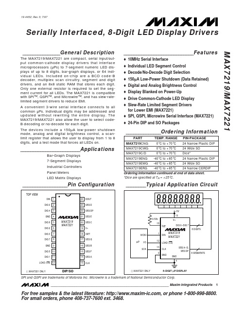
_______________General DescriptionThe MAX7219/MAX7221 are compact, serial input/out-put common-cathode display drivers that interface microprocessors (µPs) to 7-segment numeric LED dis-plays of up to 8 digits, bar-graph displays, or 64 indi-vidual LEDs. Included on-chip are a BCD code-B decoder, multiplex scan circuitry, segment and digit drivers, and an 8x8 static RAM that stores each digit.Only one external resistor is required to set the seg-ment current for all LEDs. The MAX7221 is compatible with SPI™, QSPI™, and Microwire™, and has slew-rate-limited segment drivers to reduce EMI.A convenient 3-wire serial interface connects to all common µPs. Individual digits may be addressed and updated without rewriting the entire display. The MAX7219/MAX7221 also allow the user to select code-B decoding or no-decode for each digit.The devices include a 150µA low-power shutdown mode, analog and digital brightness control, a scan-limit register that allows the user to display from 1 to 8digits, and a test mode that forces all LEDs on.________________________ApplicationsBar-Graph Displays 7-Segment Displays Industrial Controllers Panel Meters LED Matrix Displays____________________________Featureso 10MHz Serial Interfaceo Individual LED Segment Control o Decode/No-Decode Digit Selectiono 150µA Low-Power Shutdown (Data Retained)o Digital and Analog Brightness Control o Display Blanked on Power-Up o Drive Common-Cathode LED Display o Slew-Rate Limited Segment Drivers for Lower EMI (MAX7221)o SPI, QSPI, Microwire Serial Interface (MAX7221)o 24-Pin DIP and SO PackagesMAX7219/MAX7221Serially Interfaced, 8-Digit LED Display Drivers________________________________________________________________Maxim Integrated Products1________Typical Application Circuit__________________Pin Configuration19-4452; Rev 3; 7/97SPI and QSPI are trademarks of Motorola Inc. Microwire is a trademark of National Semiconductor Corp.For free samples & the latest literature: , or phone 1-800-998-8800.For small orders, phone 408-737-7600 ext. 3468.M A X 7219/M A X 72212_______________________________________________________________________________________ABSOLUTE MAXIMUM RATINGSELECTRICAL CHARACTERISTICS(V+ = 5V ±10%, R SET = 9.53k Ω±1%, T A = T MIN to T MAX , unless otherwise noted.)Stresses beyond those listed under “Absolute Maximum Ratings” may cause permanent damage to the device. These are stress ratings only, and functional operation of the device at these or any other conditions beyond those indicated in the operational sections of the specifications is not implied. Exposure to absolute maximum rating conditions for extended periods may affect device reliability.Voltage (with respect to GND)V+............................................................................-0.3V to 6V DIN, CLK, LOAD, CS ...............................................-0.3V to 6V All Other Pins.............................................-0.3V to (V+ + 0.3V)CurrentDIG0–DIG7 Sink Current................................................500mA SEGA–G, DP Source Current.........................................100mA Continuous Power Dissipation (T A = +85°C)Narrow Plastic DIP..........................................................0.87W Wide SO..........................................................................0.76W Narrow CERDIP.................................................................1.1WOperating Temperature RangesMAX7219C_G/MAX7221C_G ..............................0°C to +70°C MAX7219E_G/MAX7221E_G............................-40°C to +85°C Storage Temperature Range.............................-65°C to +160°C Lead Temperature (soldering, 10sec).............................+300°CMAX7219/MAX7221_______________________________________________________________________________________3ELECTRICAL CHARACTERISTICS (continued)(V+ = 5V ±10%, R SET =9.53k Ω±1%, T A = T MIN to T MAX , unless otherwise noted.)M A X 7219/M A X 72214_________________________________________________________________________________________________________________________________Typical Operating Characteristics(V+ = +5V, T A = +25°C, unless otherwise noted.)730750740770760790780800820810830 4.04.44.85.25.66.0SCAN FREQUENCY vs. POSITIVE SUPPLY VOLTAGEM A X 7219/21 01POSITIVE SUPPLY VOLTAGE (V)S C A N F R E Q U E N C Y (H z )20104030605070012345SEGMENT DRIVER OUTPUT CURRENTvs. OUTPUT VOLTAGEOUTPUT VOLTAGE (V)O U T P U T C U R R E N T (m A )MAX7219SEGMENT OUTPUT CURRENTM A X 7219/21 035µs/div10mA/div0MAXIMUM INTENSITY = 31/32MAX7221SEGMENT OUTPUT CURRENTM A X 7219/21 045µs/div10mA/divMAXIMUM INTENSITY = 15/16MAX7219/MAX7221______________________________________________________________Pin Description_________________________________________________________Functional DiagramM A X 7219/M A X 72216______________________________________________________________________________________________________Detailed DescriptionMAX7219/MAX7221 DifferencesThe MAX7219 and MAX7221 are identical except fortwo parameters: the MAX7221 segment drivers are slew-rate limited to reduce electromagnetic interfer-ence (EMI), and its serial interface is fully SPI compati-ble.Serial-Addressing ModesFor the MAX7219, serial data at DIN, sent in 16-bit packets, is shifted into the internal 16-bit shift register with each rising edge of CLK regardless of the state of LOAD. For the MAX7221, CS must be low to clock data in or out. The data is then latched into either the digit or control registers on the rising edge of LOAD/CS .LOAD/CS must go high concurrently with or after the 16th rising clock edge, but before the next rising clock edge or data will be lost. Data at DIN is propagated through the shift register and appears at DOUT 16.5clock cycles later. Data is clocked out on the falling edge of CLK. Data bits are labeled D0–D15 (Table 1).D8–D11 contain the register address. D0–D7 contain the data, and D12–D15 are “don’t care” bits. The first received is D15, the most significant bit (MSB).Digit and Control RegistersTable 2 lists the 14 addressable digit and control regis-ters. The digit registers are realized with an on-chip,8x8 dual-port SRAM. They are addressed directly so that individual digits can be updated and retain data as long as V+ typically exceeds 2V. The control registers consist of decode mode, display intensity, scan limit (number of scanned digits), shutdown, and display test (all LEDs on).Shutdown ModeWhen the MAX7219 is in shutdown mode, the scan oscil-lator is halted, all segment current sources are pulled to ground, and all digit drivers are pulled to V+, thereby blanking the display. The MAX7221 is identical, except the drivers are high-impedance. Data in the digit and control registers remains unaltered. Shutdown can be used to save power or as an alarm to flash the display by successively entering and leaving shutdown mode. For minimum supply current in shutdown mode, logic inputs should be at ground or V+ (CMOS-logic levels).Typically, it takes less than 250µs for the MAX7219/MAX7221 to leave shutdown mode. The display driver can be programmed while in shutdown mode, and shutdown mode can be overridden by the display-test function.Figure 1. Timing DiagramTable 1. Serial-Data Format (16 Bits)Initial Power-UpOn initial power-up, all control registers are reset, the display is blanked, and the MAX7219/MAX7221 enter shutdown mode. Program the display driver prior to display use. Otherwise, it will initially be set to scan one digit, it will not decode data in the data registers, and the intensity register will be set to its minimum value.Decode-Mode RegisterThe decode-mode register sets BCD code B (0-9, E, H,L, P, and -) or no-decode operation for each digit. Each bit in the register corresponds to one digit. A logic high selects code B decoding while logic low bypasses the decoder. Examples of the decode mode control-regis-ter format are shown in Table 4.When the code B decode mode is used, the decoder looks only at the lower nibble of the data in the digit registers (D3–D0), disregarding bits D4–D6. D7, which sets the decimal point (SEG DP), is independent of the decoder and is positive logic (D7 = 1 turns the decimal point on). Table 5 lists the code B font.When no-decode is selected, data bits D7–D0 corre-spond to the segment lines of the MAX7219/MAX7221.Table 6 shows the one-to-one pairing of each data bit to the appropriate segment line.MAX7219/MAX7221Table 3. Shutdown Register Format (Address (Hex) = XC)Table 4. Decode-Mode Register Examples (Address (Hex) = X9)M A X 7219/M A X 7221Intensity Controland Interdigit BlankingThe MAX7219/MAX7221 allow display brightness to be controlled with an external resistor (R SET ) connected between V+ and ISET. The peak current sourced from the segment drivers is nominally 100 times the current entering ISET. This resistor can either be fixed or vari-able to allow brightness adjustment from the front panel. Its minimum value should be 9.53Ω, which typi-cally sets the segment current at 40mA. Display bright-ness can also be controlled digitally by using the intensity register.Digital control of display brightness is provided by an internal pulse-width modulator, which is controlled by the lower nibble of the intensity register. The modulator scales the average segment current in 16 steps from a maximum of 31/32 down to 1/32 of the peak current set by R SET (15/16 to 1/16 on MAX7221). Table 7 lists the intensity register format. The minimum interdigit blank-ing time is set to 1/32 of a cycle.8_______________________________________________________________________________________Table 5. Code B FontTable 6. No-Decode Mode Data Bits and Corresponding Segment Lines*The decimal point is set by bit D7 = 1Scan-Limit RegisterThe scan-limit register sets how many digits are dis-played, from 1 to 8. They are displayed in a multiplexed manner with a typical display scan rate of 800Hz with 8digits displayed. If fewer digits are displayed, the scan rate is 8f OSC /N, where N is the number of digitsscanned. Since the number of scanned digits affects the display brightness, the scan-limit register should not be used to blank portions of the display (such as leading zero suppression). Table 8 lists the scan-limit register format.MAX7219/MAX7221_______________________________________________________________________________________9Table 7. Intensity Register Format (Address (Hex) = XA)Table 8. Scan-Limit Register Format (Address (Hex) = XB)*See Scan-Limit Register section for application.M A X 7219/M A X 7221If the scan-limit register is set for three digits or less,individual digit drivers will dissipate excessive amounts of power. Consequently, the value of the R SET resistor must be adjusted according to the number of digits dis-played, to limit individual digit driver power dissipation.Table 9 lists the number of digits displayed and the corresponding maximum recommended segment cur-rent when the digit drivers are used.Display-Test RegisterThe display-test register operates in two modes: normal and display test. Display-test mode turns all LEDs on by overriding, but not altering, all controls and digit reg-isters (including the shutdown register). In display-test mode, 8 digits are scanned and the duty cycle is 31/32(15/16 for MAX7221). Table 10 lists the display-test reg-ister format.No-Op RegisterThe no-op register is used when cascading MAX7219s or MAX7221s. Connect all devices’ LOAD/CS inputs together and connect DOUT to DIN on adjacent devices. DOUT is a CMOS logic-level output that easily drives DIN of successively cascaded parts. (Refer to the Serial Addressing Modes section for detailed infor-mation on serial input/output timing.) For example, if four MAX7219s are cascaded, then to write to thefourth chip, sent the desired 16-bit word, followed by three no-op codes (hex XX0X, see Table 2). When LOAD/CS goes high, data is latched in all devices. The first three chips receive no-op commands, and the fourth receives the intended data.__________Applications InformationSupply Bypassing and WiringTo minimize power-supply ripple due to the peak digit driver currents, connect a 10µF electrolytic and a 0.1µF ceramic capacitor between V+ and GND as close to the device as possible. The MAX7219/MAX7221 should be placed in close proximity to the LED display, and connections should be kept as short as possible to minimize the effects of wiring inductance and electro-magnetic interference. Also, both GND pins must be connected to ground.Selecting R SET Resistor andUsing External DriversThe current per segment is approximately 100 times the current in ISET. To select R SET , see Table 11. The MAX7219/MAX7221’s maximum recommended seg-ment current is 40mA. For segment current levels above these levels, external digit drivers will be need-ed. In this application, the MAX7219/MAX7221 serve only as controllers for other high-current drivers or tran-sistors. Therefore, to conserve power, use R SET = 47k Ωwhen using external current sources as segment dri-vers.The example in Figure 2 uses the MAX7219/MAX7221’s segment drivers, a MAX394 single-pole double-throw analog switch, and external transistors to drive 2.3”AND2307SLC common-cathode displays. The 5.6V zener diode has been added in series with the decimal point LED because the decimal point LED forward volt-age is typically 4.2V. For all other segments the LED forward voltage is typically 8V. Since external transis-tors are used to sink current (DIG 0 and DIG 1 are used as logic switches), peak segment currents of 45mA are allowed even though only two digits are displayed. In applications where the MAX7219/MAX7221’s digit dri-vers are used to sink current and fewer than four digits are displayed, Table 9 specifies the maximum allow-able segment current. R SET must be selected accord-ingly (Table 11).Refer to the Power Dissipation section of the Absolute Maximum Ratings to calculate acceptable limits for ambient temperature, segment current, and the LED forward-voltage drop.10______________________________________________________________________________________Table 9. Maximum Segment Current for 1-, 2-, or 3-Digit DisplaysTable 10. Display-Test Register Format (Address (Hex) = XF)Note: The MAX7219/MAX7221 remain in display-test mode (all LEDs on) until the display-test register is reconfigured for normal operation.Computing Power DissipationThe upper limit for power dissipation (PD) for the MAX7219/MAX7221 is determined from the following equation:PD = (V + x 8mA) + (V+ - V LED )(DUTY x I SEG x N)where:V+ = supply voltageDUTY = duty cycle set by intensity register N = number of segments driven (worst case is 8)V LED = LED forward voltageI SEG = segment current set by R SET Dissipation Example:I SEG = 40mA, N = 8, DUTY = 31/32, V LED = 1.8V at 40mA, V+ = 5.25V PD = 5.25V(8mA) + (5.25V - 1.8V)(31/32 x 40mA x 8) = 1.11WThus, for a CERDIP package (θJA = +60°C/W from Table 12), the maximum allowed ambient temperature T A is given by:T J(MAX)= T A + PD x θJA + 150°C = T A +1.11W x60°C/Wwhere T A = +83.4°C.Cascading DriversThe example in Figure 3 drives 16 digits using a 3-wire µP interface. If the number of digits is not a multiple of 8, set both drivers’ scan limits registers to the same number so one display will not appear brighter than the other. For example, if 12 digits are need, use 6 digits per display with both scan-limit registers set for 6 digits so that both displays have a 1/6 duty cycle per digit. If 11 digits are needed, set both scan-limit registers for 6digits and leave one digit driver unconnected. If one display for 6 digits and the other for 5 digits, the sec-ond display will appear brighter because its duty cycle per digit will be 1/5 while the first display’s will be 1/6.Refer to the No-Op Register section for additional infor-mation.MAX7219/MAX7221______________________________________________________________________________________11Table 11. R SET vs. Segment Current and LED Forward VoltageTable 12. Package Thermal Resistance DataM A X 7219/M A X 722112______________________________________________________________________________________Figure 2. MAX7219/MAX7221 Driving 2.3-Inch DisplaysMAX7219/MAX7221______________________________________________________________________________________13Figure 3. Cascading MAX7219/MAX7221s to Drive 16 7-Segment LED DigitsM A X 7219/M A X 722114_______________________________________________________________________________________Ordering Information (continued)___________________Chip TopographySEG FSEG ACLK LOAD OR CS DIG 1DIG 5GNDGNDDIG 7DIG 3DIG 2DIG 60.093"(2.36mm)0.080"(2.03mm)SEG B ISET SEG ESEG DP SEG CSEG G DIG 4DIG 0DIN DOUT SEG DTRANSISTOR COUNT: 5267SUBSTRATE CONNECTED TO GNDMAX7219/MAX7221______________________________________________________________________________________15________________________________________________________Package InformationM A X 7219/M A X 7221___________________________________________Package Information (continued)Maxim cannot assume responsibility for use of any circuitry other than circuitry entirely embodied in a Maxim product. No circuit patent licenses are implied. Maxim reserves the right to change the circuitry and specifications without notice at any time.16____________________Maxim Integrated Products, 120 San Gabriel Drive, Sunnyvale, CA 94086 408-737-7600©1997 Maxim Integrated ProductsPrinted USAis a registered trademark of Maxim Integrated Products.。
max7219资料及电路图
MAX7219是MAXIM公司生产的串行输入/输出共阴极数码管显示驱动芯片,一片MAX7219可驱动8个7段(包括小数点共8段)数字LED、LED条线图形显示器、或64个分立的LED发光二级管。
该芯片具有10MHz传输率的三线串行接口可与任何微处理器相连,只需一个外接电阻即可设置所有LED的段电流。
它的操作很简单,MCU只需通过模拟SPI三线接口就可以将相关的指令写入MAX7219的内部指令和数据寄存器,同时它还允许用户选择多种译码方式和译码位。
此外它还支持多片7219串联方式,这样MCU就可以通过3根线(即串行数据线、串行时钟线和芯片选通线)控制更多的数码管显示。
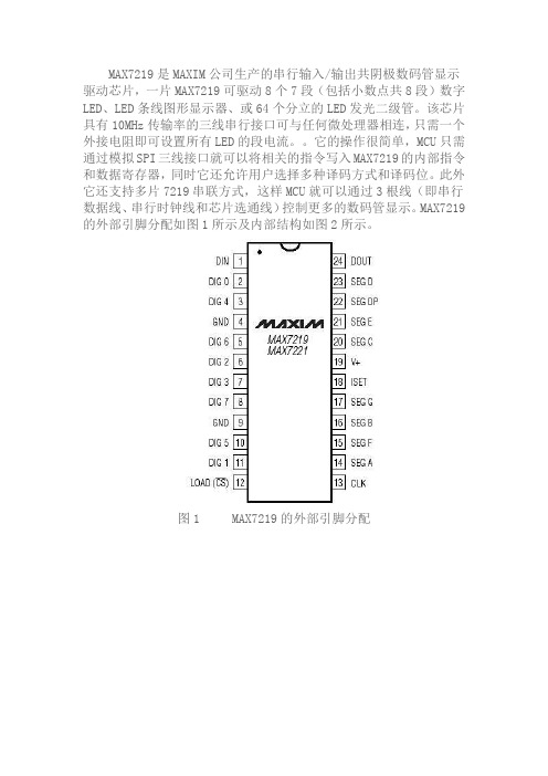
MAX7219的外部引脚分配如图1所示及内部结构如图2所示。
图1 MAX7219的外部引脚分配图2 MAX7219的内部引脚分配各引脚的功能为:DIN:串行数据输入端DOUT:串行数据输出端,用于级连扩展LOAD:装载数据输入CLK:串行时钟输入DIG0~DIG7:8位LED位选线,从共阴极LED中吸入电流SEG A~SEG G DP 7段驱动和小数点驱动ISET:通过一个10k电阻和Vcc相连,设置段电流MAX7219有下列几组寄存器:(如图3)MAX7219内部的寄存器如图3,主要有:译码控制寄存器、亮度控制寄存器、扫描界限寄存器、关断模式寄存器、测试控制寄存器。
编程时只有正确操作这些寄存器,MAX7219才可工作。
图 3 MAX7219内部的相关寄存器分别介绍如下:(1)译码控制寄存器(X9H)如图4所示,MAX7219有两种译码方式:B译码方式和不译码方式。
当选择不译码时,8个数据为分别一一对应7个段和小数点位;B译码方式是BCD译码,直接送数据就可以显示。
实际应用中可以按位设置选择B译码或是不译码方式。
图4 MAX7219的译码控制寄存器(2)扫描界限寄存器(XBH)如图5所示,此寄存器用于设置显示的LED的个数(1~8),比如当设置为0xX4时,LED 0~5显示。
点阵屏驱动程序(MAX7219)
Write_Max7219_byte(0);
Write_Max7219_byte(0);
Max7219_pinCS=1;
Write_Max7219(0,0); //清除缓冲区数据,消除显示误差
}
}
void Display_4(uchar dat)
{
uchar i;
{0x00,0x70,0x88,0x80,0x80,0x80,0x88,0x70},//C16
};
//--------------------------------------------
//功能:向MAX7219(U3)写入字节
//入口参数:DATA
//出口参数:无
//说明:
void Write_Max7219_byte(uchar DATA)
Write_Max7219_byte(0);
Write_Max7219_byte(0);
Write_Max7219_byte(0);
Write_Max7219_byte(0);
Write_Max7219_byte(0);
Max7219_pinCS=1;
Write_Max7219(0,0); //清除缓冲区数据,消除显示误差
Write_Max7219(7,0);//清除缓冲区数据,消除显示误差
Write_Max7219(8,0);//清除缓冲区数据,消除显示误差
}
/***************************************************/
void Display_1(uchar dat)
{
Write_Max7219_byte(0);
串行LED显示驱动器MAX7219及其应用

串行L ED显示驱动器M AX7219及其应用胡奕明(空军工程大学工程学院研究生大队 西安 710038)摘 要 阐述了新型显示驱动芯片M A X7219的基本工作原理和软件设计方法。
该芯片功能强大、编程简单、控显可靠,可广泛用于工业控制器等方面的数码显示驱动。
关键词 显示驱动器 串行发送 M A X72191 概 述M A X7219是美国M A X I M公司生产的串行输入 输出共阴极显示驱动器。
该芯片可直接驱动最多8位7段数字L ED显示器,或64个L ED和条形图显示器。
它与微处理器的接口非常简单,仅用3个引脚与微处理器相应端连接即可实现最高10M H z 串行接口。
M A X7219的位选方式独具特色,它允许用户选择多种译码方式译码选位,而且,每个显示位都能个别寻址和刷新,而不需要重写其他的显示位,这使得软件编程十分简单且灵活。
另外,它具有数字和模拟亮度控制以及与M O TOROLA SP I, Q SP I及M A T I ONAL M I CROW I R E串行口相兼容等特点。
2 引脚说明该芯片采用24脚D IP和SO封装,工作电压410~515V,最大功耗111W。
引脚说明见表1。
3 基本工作原理及使用方法M A X7219与8031单片机连接采用三线串行接口,典型应用电路如图1。
对于M A X7219,串行数据是以16位数据包的形式从D in脚串行输入,在CL K的每一个上升沿一位一位地送入芯片内部16位移位寄存器,而不管L out脚的状态如何。
L oad脚必须在第16个CL K上升沿出现的同时或之后,但在下一个CL K上升沿之前变为高电平,否则移入的数据将丢失。
表1 引脚说明引脚号名称功能说明1D in串行数据输入端。
在CL K的上升沿数据被锁入芯片内部16位移位寄存器2,3,5~8,10,11D IG0~D IG78位L ED位选线,从共阴极L ED中吸入电流4,9GND地线(两个GND必须接在一起)12L oad锁入输入的数据。
MAX7219
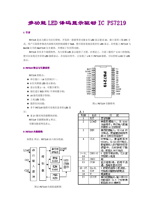
多功能LED译码显示驱动IC PS7219 1 引言PS7219是由力源公司自行研制、开发的一款新型多功能8位LED显示驱动IC。
接口采用三线SPI方式,用户只需简单修改内部相关的控制或数字RAM,便可很容易地实现多位LED显示。
在性能上PS7219与MAXIM 公司的MAX7219完全兼容,并增加了位闪等功能。
PS7219具有多个级联特性,为大屏幕LED显示提供了方便。
在理论上,只需三根用户I/O口控制线,便可以实现无穷多的LED级联显示。
在实际应用中,已实现了149片PS7219级联,可以控制1192位LED 显示。
2 PS7219特点与引脚说明PS7219的特点:★ 串行接口(16位控制字);★ 8位共阴级LED显示驱动;★ 显示位数1~8,可数字调节;★ 按位进行BCD译码/不译码数字制;★ 16级亮度数字控制;★ 上电LED全熄;★ 提供位闪功能;★ 多个PS7219级联可实现任意多的LED显示;★ 宽24脚双列直插模块封装。
PS7219引脚图如图1所示。
引脚功能说明见表1。
3 PS7219内部结构如图2 所示,PS7219由六部分组成。
图2 PS7219内部组成框图图1 PS7219引脚排列3.1 串行输入缓冲部分主要功能是与外部控制信号接口,将控制命令串行读入,并进行串并转换,供控制器读取。
3.2 控制器是整个IC的核心部分。
它先将输入缓冲部分的控制字读入处理,根据其地址值送到相应的控制RAM或数字RAM,同时将数据送入串行同步输出部分,以便在下一个控制字输入周期,将其串行输出。
3.3 控制RAM数据RAM这两部分一起控制LED译码显示部分,实现不同功能及字符的显示。
控制RAM包括:空操作寄存器,译码模式控制寄存器,亮度控制寄存器,掉电控制寄存器,闪烁控制寄存器,测试控制寄存器和扫描界线寄存器。
数据RAM包括:数据1—8寄存器。
3.4 LED译码显示根据控制RAM和数据RAM的不同值,来实现相应的显示功能。
MAX7219单片以及级联驱动程序

MAX7219单片以及级联驱动程序2011-03-20 09:40说明一下:这个word版式是从百度上下载的,在原版中,作者只是写了驱动一片MAX7219的程序。
本人作为菜鸟,第一次使用MAX7219就用了两片级联来驱动15个数码管,按照原版程序驱动一片MAX7219是没有问题的,但是,驱动两片MAX7219就不行了。
自己先认真看了MAX7219的DataSsheet,因为英语是个二把刀,看的迷迷糊糊,似懂非懂(可见英语还是很重要的),又在网上搜索也没发现有正确的程序(都是有点儿问题,上网贴出来请教各位大虾的),没办法只能自力更生了,终于调出来了。
将原版增删修改,传上来共享,希望对以后某位菜鸟第一次使用MAX7219时有所帮助啦,嘿嘿!/**************************************************************** *常用符号定义******************************************************************/#define uchar unsigned char/**************************************************************** *定义MAX7219寄存器******************************************************************/#define REG_NO_OP 0x00 //定义空操作register#define DIG_1 0x01 // 定义数码管1 register#define DIG_2 0x02 // 定义数码管2 register#define DIG_3 0x03 // 定义数码管3 register#define DIG_4 0x04 // 定义数码管4 register#define DIG_5 0x05 // 定义数码管5 register#define DIG_6 0x06 // 定义数码管6 register#define DIG_7 0x07 // 定义数码管7 register#define DIG_8 0x08 // 定义数码管8 register#define REG_DECODE 0x09 // 定义解码控制register#define REG_INTENSITY 0x0a // 定义显示亮度register#define REG_SCAN_LIMIT 0x0b // 定义扫描限制register#define REG_SHUTDOWN 0x0c // 定义"shutdown"模式register#define REG_DISPLAY_TEST 0x0f // 定义"display test"模式register#define INTENSITY_MIN 0x00 // 定义最低显示亮度#define INTENSITY_MAX 0x0f // 定义最高显示亮度/****************************************************************** * 定义硬件引脚连接******************************************************************/#define DATA P2^3; //定义P3_5连接MAX7219 DATA引脚#define CLK P2^5; //定义P3_4连接MAX7219 CLK 引脚#define CS P2^4; //定义P3_3连接MAX7219 CS 引脚/***************************************************************** * 共阴极七段数码管显示对应段查询表(数字0-9分别对应code_table[0]-[9])***********************************************************/uchar code code_table[10]={0x7e,0x30,0x6d,0x79,0x33,0x5b,0x5f,0x70,0x7f,0x7b}; /*采用数组*//****************************************************************** * MAX7219_Send()描述: 向MAX7219传送一字节数据Arguments : dataout = data to sendReturns : none******************************************************************/ void send (uchar datain){char I,temp;for (i=8; i>0; i--){CLK=0; // CLK 置低temp=datain&0x80;if (temp==0x80) // 判断并输出一位DATA=1; // 输出"1"else // 或DATA=0; // 输出"0"datain<<=1; //datain左移位,以便再次与0x80按位与CLK=1; // CLK 置高}}/**************************************************************** * MAX7219_Write()/MAX7219_Write_1()描述: 向 MAX7219 写命令Arguments : reg_number = register to write todataout = data to write to MAX7219Returns : none************************************************************** */ void MAX7219_Write (uchar add1, uchar dat1) //向第一片MAX7219写数据{CS=0; // CS置低选通MAX7219send(add1); // 写register number 到MAX7219send(dat1); // 写data 到MAX7219CS=1; // 利用CS上升沿锁存以上移位进输入的16位数据}void MAX7219_Write_1(uchar add2,uchar dat2) //向第二片MAX7219写数据{CS=0;sent(add2);sent(dat2);CLK=1; // 第16.5个时钟周期,数据从第一片MAX7219的DOUT端开始输出sent(REG_NO_OP); //对第一片MAX7219进行空操作,sent(0x00);CS=1;}/******************************************************************** MAX7219_DisplayChar()描述: 使某一位显示一个数字Arguments : digit = digit number (0-7)character = character to display (0-9, A-Z)Returns : none****************************************************************/void MAX7219_DisplayChar (char digit, char character){MAX7219_Write(digit, character);}PS:这个函数可以不要,直接调用写数据函数就可以了(原版)/******************************************************************** MAX7219_Clear()/MAX7219_clear_1()描述: 清除所有位的显示Arguments : noneReturns : none*****************************************************************/ void MAX7219_Clear (){uchar i;for (i=0; i < 8; i++)MAX7219_Write(i, 0x00); // 清除第一片MAX7219所有位的显示}void MAX7219_Clear_1(){uchar i;for(i=1;i<=8;i++)MAX7219_Write_1(i,0x00); //清除第二片MAX7219所有位的显示}PS:可以两片一起清楚数据,但建议分开较好。
MAX7219中文资料-附有程序
MAX7219是MAXIM公司生产的串行输入/输出共阴极数码管显示驱动芯片,一片MAX7219可驱动8个7段(包括小数点共8段)数字LED、LED条线图形显示器、或64个分立的LED发光二级管。
该芯片具有10MHz传输率的三线串行接口可与任何微处理器相连,只需一个外接电阻即可设置所有LED的段电流。
它的操作很简单,MCU只需通过模拟SPI三线接口就可以将相关的指令写入MAX721 9的内部指令和数据寄存器,同时它还允许用户选择多种译码方式和译码位。
此外它还支持多片7219串联方式,这样MCU就可以通过3根线(即串行数据线、串行时钟线和芯片选通线)控制更多的数码管显示。
MAX7219的外部引脚分配如图1所示及内部结构如图2所示。
图1 MAX7219的外部引脚分配图2 MAX7219的内部引脚分配各引脚的功能为:DIN:串行数据输入端DOUT:串行数据输出端,用于级连扩展LOAD:装载数据输入CLK:串行时钟输入DIG0~DIG7:8位LED位选线,从共阴极LED中吸入电流SEG A~SEG G DP 7段驱动和小数点驱动ISET:通过一个10k电阻和Vcc相连,设置段电流MAX7219有下列几组寄存器:(如图3)MAX7219内部的寄存器如图3,主要有:译码控制寄存器、亮度控制寄存器、扫描界限寄存器、关断模式寄存器、测试控制寄存器。
编程时只有正确操作这些寄存器,MAX7219才可工作。
图 3 MAX7219内部的相关寄存器分别介绍如下:(1)译码控制寄存器(X9H)如图4所示,MAX7219有两种译码方式:B译码方式和不译码方式。
当选择不译码时,8个数据为分别一一对应7个段和小数点位;B译码方式是BCD译码,直接送数据就可以显示。
实际应用中可以按位设置选择B译码或是不译码方式。
图4 MAX7219的译码控制寄存器(2)扫描界限寄存器(XBH)如图5所示,此寄存器用于设置显示的LED的个数(1~8),比如当设置为0xX4时,LED 0~5显示。
51单片机程序 MAX7219

#define LSB 0x01
//max7219 part
#define DECODE_MODE 0x09
#define INTENSITY 0x0A
#define SCAN_LIMIT 0x0B
#define SHUT_DOWN 0x0C
#define DISPLAY_TEST 0x0F
{
LOAD = LOW;
Write_Max7219_byte(address);
Write_Max7219_byte(dat);
LOAD = HIGH;
}
void Init_Max7219(void) //初始化max7219子函数设置工作寄存器需要查看芯片手册
{
Write_Max7219(SHUT_DOWN,0x01); //Normal Operation XXXXXXX1 Shutdown Mode XXXXXXXX0
Write_Max7219(SCAN_LIMIT,0x07); //SCAN LIMIT 0~7 0xX0~0xX7
Write_Max7219(INTENSITY,0x0f); //Set Intensity 0xX0~0xXf强度调节
}
void main(void)//显示1~8数字
{
unsigned char i;
void delayms(uint z)//延时函数
{
uint x,y;
for(x=z;x>0;x--)
for(y=110;y>0;y-Fra bibliotek);}
void Write_Max7219_byte(unsigned char temp)//发送一个字节的子程序,上升沿发送数据
- 1、下载文档前请自行甄别文档内容的完整性,平台不提供额外的编辑、内容补充、找答案等附加服务。
- 2、"仅部分预览"的文档,不可在线预览部分如存在完整性等问题,可反馈申请退款(可完整预览的文档不适用该条件!)。
- 3、如文档侵犯您的权益,请联系客服反馈,我们会尽快为您处理(人工客服工作时间:9:00-18:30)。
MAX7219是MAXIM公司生产的串行输入/输出共阴极数码管显示驱动芯片,一片MAX7219可驱动8个7段(包括小数点共8段)数字LED、LED条线图形显示器、或64个分立的LED发光二级管。
该芯片具有10MHz传输率的三线串行接口可与任何微处理器相连,只需一个外接电阻即可设置所有LED的段电流。
它的操作很简单,MCU只需通过模拟SPI三线接口就可以将相关的指令写入MAX7219的内部指令和数据寄存器,同时它还允许用户选择多种译码方式和译码位。
此外它还支持多片7219串联方式,这样MCU就可以通过3根线(即串行数据线、串行时钟线和芯片选通线)控制更多的数码管显示。
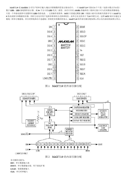
MAX7219的外部引脚分配如图1所示及内部结构如图2所示。
图1 MAX7219的外部引脚分配
图2 MAX7219的内部引脚分配
各引脚的功能为:
DIN:串行数据输入端
DOUT:串行数据输出端,用于级连扩展
LOAD:装载数据输入
CLK:串行时钟输入
DIG0~DIG7:8位LED位选线,从共阴极LED中吸入电流SEG A~SEG G DP 7段驱动和小数点驱动ISET:通过一个10k电阻和Vcc相连,设置段电流MAX7219有下列几组寄存器:(如图3)。