AK-4
PHILIPS各型 CD机的光头以及解码信息
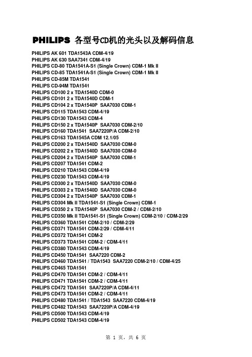
PHILIPS 各型号CD机的光头以及解码信息PHILIPS AK 601 TDA1543A CDM-4/19PHILIPS AK 630 SAA7341 CDM-4/19PHILIPS CD-80 TDA1541A-S1 (Single Crown) CDM-1 Mk IIPHILIPS CD-85 TDA1541A-S1 (Single Crown) CDM-1 Mk IIPHILIPS CD-85M TDA1541PHILIPS CD-94M TDA1541PHILIPS CD100 2 x TDA1540D CDM-0PHILIPS CD101 2 x TDA1540D CDM-1PHILIPS CD104 2 x TDA1540P SAA7030 CDM-1PHILIPS CD115 TDA1543 CDM-4/19PHILIPS CD130 TDA1543 CDM-4PHILIPS CD150 2 x TDA1540P SAA7030 CDM-2/10PHILIPS CD160 TDA1541 SAA7220P/A CDM-2/10PHILIPS CD163 TDA1545A CDM 12.1/05PHILIPS CD200 2 x TDA1540D SAA7030 CDM-0PHILIPS CD202 2 x TDA1540D SAA7030 CDM-0PHILIPS CD204 2 x TDA1540P SAA7030 CDM-1PHILIPS CD207 TDA1541 CDM-2PHILIPS CD210 TDA1543 CDM-4/19PHILIPS CD230 TDA1543 CDM-4/19PHILIPS CD300 2 x TDA1540D SAA7030 CDM-0PHILIPS CD303 2 x TDA1540D SAA7030 CDM-0PHILIPS CD304 2 x TDA1540P SAA7030 CDM-1PHILIPS CD304 Mk II TDA1541-S1 (Single Crown) CDM-1PHILIPS CD350 2 x TDA1540P SAA7030 CDM-2 / CDM-2/10PHILIPS CD350 Mk II TDA1541-S1 (Single Crown) CDM-2/10 / CDM-2/29 PHILIPS CD360 TDA1541 CDM-2/10 / CDM-2/29PHILIPS CD371 TDA1541 CDM-2/29 / CDM-4/11PHILIPS CD372 TDA1541 CDM-2PHILIPS CD373 TDA1541 CDM-2 / CDM-4/11PHILIPS CD380 TDA1543 CDM-4/19PHILIPS CD450 TDA1541 SAA7220 CDM-2PHILIPS CD460 TDA1541 / TDA1543 SAA7220 CDM-2/10 / CDM-4/25 PHILIPS CD465 TDA1541PHILIPS CD470 TDA1541 CDM-2 / CDM-4/11PHILIPS CD471 TDA1541 CDM-2 / CDM-4/11PHILIPS CD472 TDA1541 SAA7220P/A CDM-4/11PHILIPS CD473 TDA1541 CDM-2 / CDM-4/11PHILIPS CD480 TDA1541 / TDA1543 SAA7220 CDM-4/19PHILIPS CD482 TDA1543 SAA7220P/A CDM-4/19PHILIPS CD500 TDA1543 CDM-4/19PHILIPS CD502 TDA1543 CDM-4/19PHILIPS 各型号CD机的光头以及解码信息PHILIPS CD580 TDA1541PHILIPS CD581 TDA1541 CDM-4/19PHILIPS CD582 TDA1541 SAA7220P/A CDM-4/19PHILIPS CD584 TDA1541A SAA7220P/B CDM-4/19PHILIPS CD586 TDA1541A CDM-4/20PHILIPS CD600 TDA1543 SAA7220 CDM-4/19PHILIPS CD604 TDA1543 CDM-4/19PHILIPS CD605 SAA7321GP CDM-4/19PHILIPS CD610 TDA1543 SAA7220 CDM-4/19PHILIPS CD614 TDA1543 CDM-4/19PHILIPS CD615 SAA7321GP CDM-4/19PHILIPS CD618 SAA7323 CDM-4/19PHILIPS CD620 TDA1541 CDM-4/19PHILIPS CD624 SAA7321GP CDM-4/19PHILIPS CD630 TDA1541A SAA7220P/B CDM-4/19PHILIPS CD634 SAA7321 CDM-4/19PHILIPS CD640 TDA1541 SAA7220P/A CDM-2PHILIPS CD650 TDA1541 SAA7220P/A ?SAA7210 CDM-2/10 / CDM-4/25 PHILIPS CD660 TDA1541 SAA7220P/A CDM-2 / CDM-4/11PHILIPS CD67 0 TDA1541 SAA7220P/A CDM-2/10 / CDM-4/11PHILIPS CD690 SAA7341 CDM 12.1PHILIPS CD692 SAA7341GP CDM 12PHILIPS CD710 TDA1545A SAA7345 CDM 12.1PHILIPS CD720 TDA1545A CDM 12.1PHILIPS CD721 TDA1545A CDM 12PHILIPS CD722 TDA1545A VAM 1201PHILIPS CD723 TDA1545 SAA7378 VAM 1201PHILIPS CD732 SAA7341 CDM 12PHILIPS CD750 TDA1541A / TDA1549 CDM 12.1PHILIPS CD751 TDA1549 SAA7378 CDM 12.1/05PHILIPS CD753 TDA1549 SAA7378 CDM 12.1 / VAM 1201PHILIPS CD771 TDA1541 SAA7220P/A CDM-2 / CDM-4/11PHILIPS CD780 TDA1541A SAA7220 CDM-4/19PHILIPS CD782 TDA1541 SAA7220P/A CDM-2 / CDM-4PHILIPS CD820 TDA1541A SAA7220 CDM-4/19PHILIPS CD824 SAA7321GP CDM-4/19PHILIPS CD830 TDA1541A-R1 SAA7220P/B CDM-4/CompositePHILIPS CD834 SAA7321GP CDM-4/19PHILIPS CD840 2 x SAA7321GP SAA7220P/B CDM-4/19PHILIPS CD850 2 x SAA7321GP SAA7220P/B CDM-4/19PHILIPS CD850 Mk II SAA7350 CDM-4/19PHILIPS CD880 TDA1541A-S1 (Single Crown) CDM-1 Mk IIPHILIPS 各型号CD机的光头以及解码信息PHILIPS CD910 SAA7341GP CDM 12.1/05PHILIPS CD911 SAA7341GP CDM 12.1/05PHILIPS CD920 SAA7341GP CDM 12.1/05PHILIPS CD930 SAA7350 CDM-9/44PHILIPS CD931 SAA7350 CDM-9/65PHILIPS CD940 SAA7350GP SM5840AS CDM-9/44PHILIPS CD950 TDA1547 SAA7350 CDM-9/44PHILIPS CD951 TDA1547 span lang=EN-US> SAA7350 ?SAA7310 CDM-9/65 PHILIPS CD960 TDA1541 SAA7220 ?SAA7210 CDM-1PHILIPS CDC 486 TDA1543 CDM-4/20PHILIPS CDC 745 SAA7341GP CDM 12.1/05PHILIPS CDC 875 TDA1541A CDM-4/19PHILIPS CDD 461 TDA1543 CDM-4/19PHILIPS CDR 950 AD1855PHILIPS DAC 960 1 x TDA1541A DACPHILIPS LHH100M TDA1547 SM5840 CDM-9PHILIPS LHH200R TDA1547 (DAC7) CDM-9PHILIPS LHH300 SAA7321 CDM-9PHILIPS LHH300R TDA1547 (DAC7) SAA7350 CDM-9PHILIPS LHH500 2 x SAA7321GP ?SAA7220P/B CDM-4 MetallicPHILIPS LHH500R 1 x TDA1547 SM5803AP CDM-4 MetallicPHILIPS LHH600 TDA1547 (DAC7) CDM-4 MetallicPHILIPS LHH700 2 x TDA1547 SM5803APT CDM-4 MetallicPHILIPS LHH800R 1 x TDA1547 (DAC7) SM5803APT CDM-4 Metallic PHILIPS LHH900R 1 x TDA1547 (DAC7) CDM-4 MetallicPHILIPS LHH1000 TDA1541A-S1 (Double Crown) CDM-1PHILIPS LHH2000 2 x TDA1540P SAA7030 CDM-0 / CDM-1Philips的生产年份:Philips CD100: 1982Philips CD101: ?Philips CD104: 1984Philips CD110: ?Philips CD130: 1991Philips CD140: 1991Philips CD150: 1985Philips CD151: 1986Philips CD160: 1986Philips CD200: 1983Philips CD202: 1984Philips CD204: 1984Philips CD207: 1987PHILIPS 各型号CD机的光头以及解码信息Philips CD210: 1990Philips CD230: ?Philips CDC250: 1991Philips CD300: 1983Philips CD303: 1984Philips CD304: 1984: 1985Philips CD304II: 1987Philips CD320: 1991Philips CD335: 1992Philips CD345: 1992Philips CD350: 1985Philips CD351: 1986Philips CD360: 1987Philips CD372: 1988Philips CD373: 1988Philips CD380: 1989Philips CD450: 1986Philips CD460: 1987Philips CD471: 1988Philips CD472: 1988Philips CD473: 1988Philips CD480: 1989Philips CD482: ?Philips CDC486: 1989Philips CD500: ?Philips CD502: ?Philips CDC550: ?Philips CDC552: 1992Philips CDR560: 1999Philips CD582: 1989Philips CD584: ?Philips CD600: 1990Philips CD604: 1991: 1992Philips CD605: 1991Philips CD610: 1990Philips CD614: 1991: 1992Philips CD615: 1991Philips CD620: 1990Philips CD624: 1991Philips CD630: 1989PHILIPS 各型号CD机的光头以及解码信息Philips CD634: 1991Philips CD640: 1987Philips CD650: 1986: 1987Philips CD660: 1987Philips CD670: 1987Philips CD680: 1988Philips CD690: 1993Philips CD692: 1993Philips CD710: 1994Philips CD711: 1995: 1996: 1997: 1998Philips CD713: 1999Philips CD720: 1994Philips CD721: 1995: 1996: 1997Philips CD722: 1998Philips CD723: 1999Philips CD740: 1994: 1995Philips CDC745: 1994Philips CD750: 1994: 1995Philips CD751: 1995: 1996: 1997: 1998Philips CDC751: 1996: 1997Philips CDC752: 1998: 1999Philips CD753: 1999Philips CDR760: 1999Philips CDR765: 1999Philips CD771: 1988Philips CDC775: 1999Philips CD780: 1989: 1990Philips CD781: 1989: 1990Philips CD782: 1988: 1989Philips CD820: 1989.Philips CD824: 1990.Philips CD830: 1989.Philips CD834: 1990.Philips CD840: 1990Philips CD850: 1991Philips CD850II: ?Philips CDR870: 1998Philips CDC875: 1989Philips CDR880: 1999Philips CDD882: 1989Philips CD910: 1993Philips CDI910: 1991PHILIPS 各型号CD机的光头以及解码信息Philips CD911: 1994 1995 1996Philips CD916: 1995Philips CDC916: 1994 1995 1996Philips CD920: 1993Philips CDC925: 1993Philips CD926: 1995 1996Philips CDC926: 1995Philips CD930: 1993Philips CD931: 1994 1995 1996Philips CDC935: 1993: 1994Philips CD936: 1995: 1996Philips CDC936: 1995Philips CD940: 1993Philips CD950: 1993Philips CD951: 1994 1995 1996Philips CD960: 1987 1988。
DF4、DF7电器试验(路局)(1)
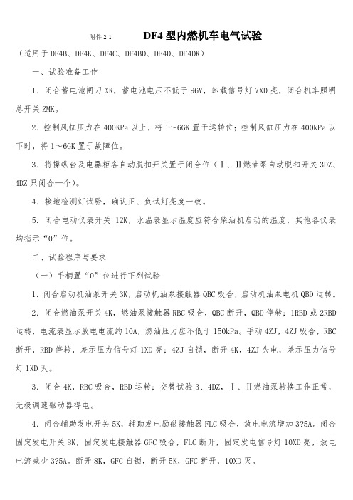
附件2-1 DF4型内燃机车电气试验(适用于DF4B、DF4K、DF4C、DF4BD、DF4D、DF4DK)一、试验准备工作1.闭合蓄电池闸刀XK,蓄电池电压不低于96V,卸载信号灯7XD亮,闭合机车照明总开关ZMK。
2.控制风缸压力在400KPa以上,将1~6GK置于运转位;控制风缸压力在400kPa以下时,将1~6GK置于故障位。
3.将操纵台及电器柜各自动脱扣开关置于闭合位(Ⅰ、Ⅱ燃油泵自动脱扣开关3DZ、4DZ只闭合—个)。
4.接地检测灯试验,确认正、负试灯亮度一致。
5.闭合电动仪表开关12K,水温表显示温度应符合柴油机启动的温度,其他各仪表均指示“0”位。
二、试验程序与要求(一)手柄置“0”位进行下列试验1.闭合启动机油泵开关3K,启动机油泵接触器QBC吸合,启动机油泵电机QBD运转。
2.闭合燃油泵开关4K,燃油泵接触器RBC吸合,QBC断开,QBD停转;1RBD或2RBD 运转,电流表显示放电电流约10A,燃油压力应不低于150kPa。
手动4ZJ,4ZJ吸合,RBC 断开,RBD停转,差示压力信号灯1XD亮;4ZJ自锁,断开4K,4ZJ失电,差示压力信号灯1XD灭。
3.闭合4K,RBC吸合,RBD运转;交替试验3、4DZ,Ⅰ、Ⅱ燃油泵转换工作正常,无极调速驱动器得电。
4.闭合辅助发电开关5K,辅助发电励磁接触器FLC吸合,放电电流增加3?5A。
闭合固定发电开关8K,固定发电接触器GFC吸合,FLC断开,固定发电信号灯10XD亮,放电电流减少3?5A。
断开8K,GFC自锁,断开5K,GFC断开,10XD灭。
5.闭合5K,FLC得电,手按辅助发电过流保护继电器FLJ,GFC吸合,FLC断开,固定发电信号灯10XD亮,GFC自锁;断开5K,GFC断开,10XD灭。
6.闭合空压机自动控制开关10K,YC吸合(总风缸压力低于750KPA)空压机启动信号灯6XD亮,延时2?3S,YRC吸合,空压机启动信号灯6XD灭。
高中数学选修一第4章4.3~4.4数列,极限,归纳法-知识点

1高中数学选修一第4章4.3~4.4数列/极限/归纳法-知识点 1、对于以a 为首项,q 为公比的无穷等比数列{a n }.①若{a n }是绝对值递减 的数列,∞→n lim n a = 0 ,各项和∞→n lim n S =q 1a - 。
②若q=1,{a n }是常 数列,∞→n lim n a = a ,各项和∞→n lim n S 不存在 。
③若q=-1,{a n }是摆动 数列,∞→n lim n a 不存在,各项和∞→n lim n S 不存在。
{a n }是绝对值增大 的数列,∞→n lim n a = 不存在,各项和∞→n lim n S 不存在 。
2、题型:在公式S=q 1a 1-中,已知其中任意两个量,求第三个量的值或范围。
典例:设数列{a n }是公比0<q <1的等比数列,其各项和是4,求首项a 1的取值范围。
想:∵S=q 1a 1-,所以a 1=4(1-q)∈(0,4)∪(4,8)。
3、对于数列{a n },如果a n+1≥a n 恒成立,则是 增 数列,如果a n+1>a n 恒成立,则是 严格增 数列;如果a n+1≤a n 恒成立,则是 减 数列,如果a n+1<a n 恒成立,则是 严格减 数列。
增数列和减数列统称为 单调 数列。
数列的单调性的判断:①作差法,判断 a n+1-a n 的 符号 ;②对于正数数列,判断与 1 的大小关系。
4、在数列{a n }中,若a n 最大,则a n ≥ a n-1 且a n ≥ a n+1 ;若a n 最小,则a n ≤ a n-1 且a n ≤ a n+1 (n ≥2).5、数列{a n }中,前n 项和为S n ,通项公式为a n ,则a n =⎩⎨⎧≥-=2n 1n 1-n n 1,,S S S .6、由递推公式求通项公式的常用方法.①累加法,适用于类等差数列,有a n+1-a n =f(n)条件的数列。
例.a 1=0,a n+1=a n +(2n-1). ②累乘法,适用于类等比数列,有a n+1/a n =f(n)条件的数列。
常用金属材料中外牌号对照

中 国英 国日 本法 国德 国原苏联GB (YB )AISI SAEB.S.JIS NFDIM(ГOCT)碳素结8EN2A/1S9CK 8构钢08FEN2A/1SPCH108КП10EN2A S10C XC10C10,CK101010FEN2ASPH210КП15EN2E S15C XC12C15,CK151515F EN2B 15КП20EN3A S20C XC18C20,C222020F EN2C SPH320КП30EN4S30CXC323045C10121010EN8S45C XC45C45,CK4545C10101010C10151015C10201020C10201020C10301030C10451045合金结15Mn C11151115En14A SB46XC1214Mn414Г构钢20MnC10221022En3C,4S21—XC18—20Г30MnC10331033En5D,En5K —XC32—30Г50MnC10521052En43A,En 43B,En43—XC48—50Г1006分类美 国1008常用金属材料中外牌号对照1.黑色金属材料牌号对照(表8—65)表8—65 黑色金属材料牌号对照20Mn2En41A,S92,S514——20Mn520Г23T35,3T4530Mn2S92,S514,3T35,3T45—32M530Mn530Г240Mn2~En15A—40M5—40Г250Mn2~55M5—50Г220MnV ———20MnV6—42MnV ———42MnV7—15Cr ~En206SCr2112C315Cr315X 20Cr En207SCr2218C320Cr420X 40Cr En18,S117SCr438C441Cr440X 50CrEn48———50X5115中 国英 国日 本法 国德 国原苏联GB (YB )AISI SAEB.S.JIS NF DIM (ГOCT)合金结15CrMn——16MC516MCr515X Г,18X Г构钢20CrMn ——20MC520MCr520X Г40CrMn ————40X Г25CrMnSi ————25X ГC 30CrMnSi————30X ГC13,201,321—13301340分类美 国—51205140—————(续)51,505,15235CrMnSiA————35XГCA 20CrV22CrV420Xф40CrV42CrV440XфA 45CrV En5018CrMnTi18XГT 30CrMnTi30XГT 40CrMnTi40XГT12CrMo1501-620CrB12CD413CrMo4412XM20CrMo CDS12,CDS110SCM2218CD420CrMo520ХM 30CrMo SCM230ХM 35CrMo En19B SCM3 35CD434CrMo435ХM22CrMnMo40CrMnMoEn19C18XГM24CrMoV24CrMoV5538XГM,40XГM35CrMoV35CrMoV535XMфA30Cr2MoV En40C,S10630CD1230CrMoV9~25X2Mф25Cr2Mo1VA ~25X2Mф30Cr2Ni2 WVA 30X2HBфA38CrMoAlAEn41B SACMI45CAD6-1234CrAlMo538XMЮA ~411938CrWVAlAEn40C38 XBфЮA 61206140—61454118 411938CrAlA 34CrAl 38X ЮAE4132E4135中 国英 国日 本法 国德 国原苏联GB (YB )AISI SAEB.S.JIS NF DIM (ГOCT)12CrNi2ASNC2116NC1114NiCr1012XH2A 12CrNi3A En36A,En36B SNC2214NC1214NiCr1412XH3A 12Cr2Ni4A En39A,En 39B12NC1512X2H4A30CrNi3A SNC230NC1128NiCr1030XH3A37CrNi3A 37XH3A18Cr2Ni4WA18XHBA 40CrNiW 40CrHBA 30Cr2Ni2WVA30X2H2B фA40CrNiMo A En110,S95,S118SNCM835NCD536CrNiMo 440XHMA40B45B40MnB45MnB20CrMnB 20X ГP40CrMnB 40X ГP65En43E SUP2,SW R7XC65CK676575SUP3,SW R9~XC70,XC80C75,MK757560Mn En43J 60Г60SiMnEn45ASUP660SiMn660C Г4130~411941406470E(AMS)分类美 国合金结构钢E3310,3310,3310H 2515,2515H 3435~TS14B35H ~TS14B50H 50B2050B40H4340~TS14B3550B46H C10651065(续)65Mn En43E65Г50Si2Mn ~45S751Si750C2106055Si2MnEn45,142955S655Si755C2C1065106550CrVAEn47SUP1050CV450CrV450X фAT7A XC65 fins C70W1у7A T8D1SKU3XC85coura ntsC85W2у8XC85 fins T8AXC85 fins C85W1у8A T10D1SK3XC95finsC100W2у10中 国英 国日 本法 国德 国原苏联GB (YB )AISI SAE B.S.JISNF DIM (ГOCT)碳素工T10A XC95extra -fins C100W1у10A 具钢T12D1SK2,SKU2XC120fins C115W2у12T12A XC120extr a-fins C110W1у12A T8MnA SK5C85WSу8ГA 合金工9Mn2V 80M890MnV8具钢6SiCr 64SiCr56XC 9SiCr 90CrSi59XC 4SiCrV 45SiCrV64XC Cr2100C6105Cr5X Cr06SKS8110Cr2X05Cr12Steel for clod SKD1Z200C12X210Cr12X12working AlCrMn80M8145Cr6X Г5CrMnMo SKT555NCD7-0340CrMnM o75X ГM 5CrNiMo SKT465NCDV06-0255NiCrMo V65XHMCrWS SKS1120WC45-02X130W5XB5Cr12WSKD 2~X210CrW 123Cr2W8V AlW-Cr SKD5Z30WC09-03X30WCrV 9-33X2B8CrWMnSteel for clod SKS3180M8105WCr6working CXB Г5CrW2Si SKS41~45WC20-405XB2CCr12MoV Type (A)2SKD11Z200C12X165CrMoV12X12MWSKU8100WC15-04~120W4B1弹簧钢1074926092556150碳素工具钢W1-0.8C W1-0.8C-Special W1-1.0CW1-1.2C- Special2分类美 国W1-1.0C-Special W1-1.2C L4V1G(AMS)L1D3L6D 6~H21F1(续)W2SKS7115W8B2W9Cr4V2(A)14%W SKH6Z70WD12ABCP9W18Cr4V (A)18%W SKH2Z80W18S18-0-1,B18P18,P ф1W12Cr4V 4MoZ125WV,15-W S112-1-4,EV4P9ф5,P14ф4W6Mo5Cr4V2SKH93343W2Mn9Cr 4VCo8中 国英 国日 本法 国德 国原苏联GB (YB )AISI SAE B.S.JIS NFDIM(ГOCT)1Cr17Mn6Ni5NSUS20112X17Г9AH41Cr18Mn8Ni4284S16SUS20212X17Г9AH42Cr13Mn9Ni420X13H4Г91Cr17Ni7301S21SUS301Z12CN17.071Cr17Ni8SUS301JI X12CrNi1771Cr18Ni9302S25SUS302Z10CN18.09X12CrNi18812X18H91Cr18Ni9S i3SUS302B 0Cr19Ni9304S15SUS304Z6CN18.0X5CrNi1808X18H1000Cr9Ni11304S12SUS304L Z2CN18.0X2CrNi1803X18H110Cr19Ni9SUS304N10Cr19Ni10NbNSUS304N200Cr18Ni10N SUS304LN Z2CN18.10NX2CrNiN18101Cr18Ni12305S19SUS305Z18CN18.12X5CrNi181112X18H12T0Cr23Ni13SUS309S 0Cr25Ni20SUS310S0Cr17Ni12Mo2316S16SUS316Z6CND17.12X5CrNiMo 181008X17H13M2T00Cr17Ni14Mo2316S12SUS316L Z2CND17.12X2CrNiMo 181003X17H13M20Cr17Ni12Mo2N SUS316N00Cr17Ni13Mo2N SUS316LN Z2CND17.12NX2CrNiMo N18120Cr18Ni12Mo2Ti 320S17Z6CNDT17-12X10CrNiM oTi181008X17H13M2T1Cr18Ni12Mo2Ti 10X17H13M2T 0Cr18Ni12Mo2Cu2SUS316JI 00Cr18Ni14Mo2Cu2SUS316JIL高速钢T7T1M2M42分类美 国 锈201,S2*******,S2*******,S3*******B,S3*******,S3*******L,S0*******N,S30451XM21,S30452305,S30500301,S3*******S,S3*******S,S3*******,S3*******L,S31603(续)316N,S316510Cr18Ni12Mo3Ti Z6CNDT17-1308X17H15M3T1Cr18Ni12Mo3Ti 10X17H13M3T0Cr19Ni13Mo3317S16SUS31708X17H15M3T00Cr19Ni13Mo3317S12SUS317LZ2CND19.15X2CrNiMo 181603X16H15M3中 国英 国日 本法 国德 国原苏联GB (YB )AISI SAEB.S.JIS NFDIM(ГOCT)0Cr18Ni16Mo5SUS317JI0Cr18Ni11Ti321S20SUS321Z6CNT18.10X10CrNiTi 18908X18H10T1Cr18Ni9T iX10CrNiTi 18912X18H10T0Cr18Ni11N6347S17SUS347Z6CNNb18.10X10CrNiN b18908X18H12T 0Cr18Ni13Si4SUSXM15JI00Cr18Ni5Mo3Si21Cr18Ni11Si4AlTi 15X18H12-C4T101Cr21Ni5T 1X21H5T0Cr21Ni5Mo2SUS329JI 0Cr13Al 405S17SUS405Z6CA13X7CrA11300Cr12SUS410L 1Cr15SUS4291Cr17430S15SUS430Z8C17X8Cr1712X1700Cr17434S19SUS430LX 1Cr17Mo SUS434Z8CD17.0X6CrMo1700Cr17Mo SUS436L 00Cr18Mo 2SUS44400Cr30Mo 2SUS447J100Cr27Mo SUSXM27Z01CD26.1Cr12403S17SUS4031Cr13410S21SUS410Z12C13X10Cr1312X130Cr13SUS410S Z6C13X7Cr1308X132Cr13420S37SUS420J1Z20C13X20Cr1320X133Cr13420S45SUS420J230X133Cr16SUS429J1分中 国美 国英 国日 本法 国德 国原苏联不 锈 钢分类美 国317,S3*******L,S31703405,S4*******,S4*******,S43000不 锈 钢321,S32100347,S34700XM15,S38100XM27,S4*******,S40300410434,S4340018Cr2Mo410S,S4*******,S42000(续)2.有色金属材料牌号对照(表8—66)表8—66 有色金属材料牌号对照类GB(YB)ASTM,(SAE) B.S.JIS NF DIMГOCT工1070A10801A A1080A00业106010,701,060A1070(A199.6)A0纯1050A EC10501B A105A5A199.5A1铝10351030AД1 120011001C A1100A4A99A2 8A061200A1200AД防5040Д12锈5A025052N4A-5052A-G2AlMg2AMГ铝5A035154N5A-5154A-G3AlMg3AMГ3 5A055056N6A-5056A-G5AlMg5AMГ55A06AMГ6N7AMГ75056N6A-5056A-G5AlMg5AMГ5П5356AMГ5B 3A213003N3A-3003A-M1AlMn AMЦ硬2A012117L86A2117A-U2G AlCuMg0.5Д18П铝2A02BД17Д3П2A04Д19П2A06Д19Д2 2B112017A2017A-U4G AlCuMg1Д1П2B122024H14A2024A-U4G1AlCuMg2Д16П2A10B652A112017DTD A2017A-U4G AlCuMg1Д12A122024A2024A-U4G1AlCuMg2Д162A13AM42A162219A-U6MTД202A172021Д21锻6063H9A6063A-GS AlMgSi0.5AЛД铝6A026061H20A6061AlMgSiCu AB 2A50AK62B50H11AK6-12618H16A2N01A-U2GN AK4-1 2A80A-U2N AK42A902018A2018A-U4N AK22A142014H15A2014A-U4SG AlCuSiMg AK8超7A03B94硬7A047075A7075A-Z5GU AlZnMg1.5B95铝7076B95-17049A-Z8GU B967A097075A7075A-Z5GU AlZnMgC u1.5变MB1AIMIA DTD737,142,118MA1形MB2AZ31C MAG111M1MgAl3Zn MA2镁MB3MA2-1合MB4AZ61A MAG121M2MgAl6Zn MA3金MB6MA4 MB7A280X88B AZ61A MgAl7Zn MA5MB8AZ80A AM537MA8MB15AK60A DTD5031,5041AK60A BM65-1工TA1Ti-35A IMI115KS50BT1-0业TA2Ti-50A IMI125KS60BT1-1纯TA3Ti-65A IMI135KS85BT1-2钛钛TA4Ti-2Al48-T2合TA548-OT3金TA6BT5 TA7Ti-5Al-2Sn IMIB6KS115AS BT5-1TA8BT10TB1BT15钛TB2合TC1IMI315OT4-1金TC2OT4 TC3BT6CTC4Ti-6A-4V IMI137T-A6V BT6TC5BT3TC6BT3-1TC7AT6TC8BT8TC9BT9TC10Ti-6A-6V-2SnT-A6V6Sn2T3M2 T4M3 TU1101EOFCuP MB1 TU2102C103OF-CuP MB2黄H90220DTD713,CZ101RBs2Ms90Л90铜H80240DTD711,CZ103RBs4Ms80Л80H70260CZ106BsP1Ms70Л70H62280CZ119Bs3Л62 HPb63-3353216Ms63PЛC63-3 HPb59-1CZ111PbBs13Ms58ЛC59-1 HSn70-1443CZ112BsTF1SoMs71ЛO70-1 HSn62-1462NbsBE1ЛO62-1HAl60-1-1ЛAЖ60-1-1HMn58-2ЛMЦ58-2HFe59-1-1ЛЖМЦ59-1-1青QSn4-3MSnBZ4БРОЦ4-3铜QSn4-4-4B139BZ BC6MSnBZ4PbБРОЦC4-4-4QSn6.5-0.1B139,B159407-3SnBZ6БРОФ6.5-0.15QSn6.5-0.4519PBB2БРОФ6.5-0.4QSn7-0.2БРОФ7-0.2铜QAl9-2БРAMЦ9-2QAl9-4AB1БРAЖ9-4QAl10-3-1.5БРAЖM Ц10-3-1.5QAl10-4-4AMS46402033AB5NiAlBZ БРAЖH10-4-4QBe2172BeCu2БРБ2QBe1.7170BeCuP1БРБHT1.7QBe1.9БРБHT1.9序号中日板材类别日本标准牌号备注SPCSPCC普通用途冷轧板或带SPCD拉深用深拉深用SPCEN深拉深用(无时效)SPHSPHC普通用途热轧钢板(带)SPHD拉深用SPHE深拉深用冷轧不锈钢板(带)SUS××CP(SUS××CS)××为具体钢种代号数热轧不锈钢板(带)SUS××HP(SUS××HS)字(下同)SPGSPG1一般用途SPG2弯曲加工用SPG3拉深用SPG4结构件用SPTSPTE电镀锡板SPTE-D差后电镀锡板1冷轧薄钢板2热轧薄钢板(带)表8—67 中日板(带)材表示方法对照34镀锌薄钢板5镀锡薄钢板3. 中日板(带)材表示方法对照(表8—67)SPTH 热电镀锡板冷轧电工钢板S ××热轧电工钢板S ××F 铝板A ××P 铝带A ××R-0材软质-硬H 材硬-硬H 材铝板-硬质铝带H 材冷轧后自然时效-H 材-R 材铜板(带)纯铜板(带)RBSP (RBSR )黄铜板(带)BSP (BSR )磷青铜板(带)PBP (PBR )锌白铜板(带)NSP (NSR )白铜板(带)CNP (CNR )9钛板TP 678板。
AK4399中文资料
No internal bonding.
-
Connect to GND.
Right channel Common Voltage Pin,
-
Normally connected to VSS with a 10uF electrolytic cap.
O Rch Positive Analog Output Pin
I Control Data Input Pin in Serial Control Mode
I Digital Input Format 0 Pin in PCM Mode
I Chip Address 1 Pin in Serial Control Mode
I Digital Input Format 1 Pin in PCM Mode
No internal bonding.
-
Connect to GND.
I Rch Audio Serial Data Input Pin
(Internal pull-down pin)
I Lch Audio Serial Data Input Pin
(Internal pull-down pin)
36 NC
37 NC
38 NC
39 NC 40 VSS3 41 AVDD 42 MCLK 43 VSS4 44 NC
Parallel or Serial Select Pin
(Internal pull-up pin)
I
“L”: Serial Control Mode, “H”: Parallel Control Mode
13 NC
I/O
Function
- Digital Power Supply Pin, 4.75 ∼ 5.25V
上汽大众全新途观返修电路图-电动座椅调节装置,不带记忆功能
507 螺栓连接(30),在蓄电池保险丝座上
B467 连接 3,在主导线束中
B482 连接 18,在主导线束中
2.5 rt/ws
2.5 rt/ws
9911
T10f /9
4.0 rt/ws
3355
1
2
3
4
5
6
7
8
9
10
11
12
13
14
592-016020413
ws = 白色 sw = 黑色 ro = 红色 rt = 红色 br = 褐色 gn = 绿色 bl = 蓝色 gr = 灰色 li = 淡紫色 vi = 淡紫色 ge = 黄色 or = 橘黄色 rs = 粉红色
72
73
74
75
76
77
78
79
80
81
82
83
84
592-016070413
ws = 白色 sw = 黑色 ro = 红色 rt = 红色 br = 褐色 gn = 绿色 bl = 蓝色 gr = 灰色 li = 淡紫色 vi = 淡紫色 ge = 黄色 or = 橘黄色 rs = 粉红色
04.2013
31
32
33
34
35
36
37
38
39
40
41
42
592-016040413
ws = 白色 sw = 黑色 ro = 红色 rt = 红色 br = 褐色 gn = 绿色 bl = 蓝色 gr = 灰色 li = 淡紫色 vi = 淡紫色 ge = 黄色 or = 橘黄色 rs = 粉红色
04.2013
全新途观
电动座椅调节装置,不带记忆功能
AK7844资料

元器件交易网AKEMD AKEMD CONFIDENTIAL [AK7844]AK7844Stereo Audio Class-D Amp with Power Booster for Piezo SpeakersGENERAL DESCRIPTIONTHE AK7844 is Stereo Class-D amplifier for driving Piezo-Electric Speakers. Built-in Boost DCDC converter generates adequate high voltage for driving Piezo Speakers from Li-Ion battery. AKM state-of-the-art filter-less solution eliminates LC-filters, which are normally required at Class-D outputs. That contributes to total space saving. Class-D operation ensures higher power efficiency, and couple with Piezo Speaker that is low-powerconsumption and low-profile figure. The AK7844 is very applicable for cellular phones with piezo speakers.FEATURES □ Class-D Amplifier : • Piezo-Electric Speaker Driver • Single-ended analog Input • BTL output • Output voltage = 8Vrms @VDD1=8.75V • Filter-less solution • Stereo mode • Pop noise suppressor • Output short protection □ Boost DCDC Converter : • Input voltage (Battery) = 2.7V ∼ 4.5V • Over-current protection • Over-voltage protection Boosted voltage will be 8.75V□ Control function : • Pre-gain amplifier −6dB ∼ +15dB, 3dB step • Built-in Second order lowpass filter at Input. • Cutoff Frequency (4kHz,8kHz,16kHz) • Power-on/off control • Over-temperature protection □ Operational voltage* Adjustable by Pin (PG0, PG1 and PG2) control* Adjustable by Pin (PG0, PG1 and PG2) control: VBAT=2.7V ∼ 4.5V、DVDDI=1.65V ∼ 4.5V : −30°C ∼ 85°C□ Operational temperature □ Package: 31pin WL-CSP (3.0mm × 3.0mm, 0.5mm pitch)Rev.00-1–2007/08元器件交易网AKEMD AKEMD CONFIDENTIAL [AK7844]BLOCK DIAGRAMFC1 FC0 PG 2 PG 1 PG 0 DVDDI PDNVBATPower BoosterVCOIL VFB ERRO VSS3VDD1 INLPre GainLFc: 4/8/16kHzLPF LClass-D AMP LVCLN VCLP VSS1-6 ~ +15dB 3dB stepVSS4 VDD2 VCRN VCRP VSS2INRPre GainR VREFLPF RClass-D AMP RVCFigure 1. BLOCK DIAGRAMRev.00-2–2007/08元器件交易网AKEMD AKEMD CONFIDENTIAL [AK7844]PIN ASSIGNMENTA B C D E F6543.0mm3210.250.50.25<TOP VIEW>6 5 4 3 2 1A NC VCRP ERRO PG2 VCOIL NCB VDD2 VCRN VSS2 VSS4 VSS3 <Index>C D VFB NC NC NC - - - - PG1 FC1 PG0 DVDDI Figure 2. Pin AssighnmentE VDD1 VCLN VSS1 VBAT FC0 PDNF NC VCLP INL INR VC NCRev.00-3–2007/08元器件交易网ASAHI KASEIAKM CONFIDENTIAL[AK7844]Pin / FUNCTIONFunction No Connection pin. Connect to ground. Inductor pin for Boost DCDC. Pre Gain setting pin2 (available when I2CEN=”L”) Phase compensation capacitor connection pin for Boost DCDC. A4 ERRO Connect a 0.1µF capacitor between VC pin and ground. A5 VCRP O Right channel Class D amp plus output (+) A6 NC No Connection pin. Connect to ground. B1 - - <Index> B2 VSS3 - Power Booster ground pin:VSS3=0V B3 VSS4 Internal analog circuit ground pin:VSS4=0V B4 VSS2 I Right channel Class D amp ground pin:VSS2=0V B5 VCRN O Right channel Class D amp minus output (-) B6 VDD2 Right channel Class D amp power supply:VDD2=8.75V(typ.) C1 PG0 I Pre Gain setting pin0 C2 PG1 I Pre Gain setting pin1 C3 - - - C4 - - - C5 NC No Connection pin. Connect to ground. C6 VFB Boosted voltege feedback pin. D1 DVDDI Digital interface power:DVDDI=1.65V~4.5V D2 FC1 I SCF cutoff frequency setting pin1 D3 - - - D4 - - - No Connection pin. Connect to ground. D5 NC No Connection pin. Connect to ground. D6 NC Power down contorol:schmitt trigger input E1 PDN I “High”:poewer up、”Low”:power down SCF cutoff frequency setting pin2 E2 FC0 I Battery voltage input:VBAT=2.7V~4.5V E3 VBAT - Left channel Class D amp ground pin:VSS1=0V E4 VSS1 - Left channel Class D amp minus output (-) E5 VCLN O Left channel Class D amp power supply:VDD1=8.75V(typ.) E6 VDD1 F1 NC No Connection pin. Connect to ground. Voltage reference output. Connect a 0.01µF capacitor between VC pin and ground. F2 VC F3 INR I Right channel analog signal input F4 INL I Left channel analog signal input F5 VCLP O Left channel Class D amp plus output (+) F6 NC No Connection pin. Connect to ground. Note 1. Digital input pins (PDN, PG2, PG1, PG0, FC1, FC0) must not be open. No. A1 A2 A3 Pin Name NC VCOIL PG2 I/O - - IUnused Pins Unused pins should be configured as below. Category Pin Name NoConnection NCConfiguration GNDRev.01-4–2007/08元器件交易网ASAHI KASEIAKM CONFIDENTIAL[AK7844]ABSOLUTE MAXIMUM RATINGS (VSS1, VSS2, VSS3,VSS4=0V;Note 3) Parameter Symbol min max Power Supplies: Battery VBAT −0.3 6.5 (Note.4) Digital I/F DVDDI −0.3 6.5 Class-D Amp VDD1,2 −0.3 15 Input Current, Any Pin Except Supplies IIN -10 +10 Analog Input Voltage (Note 4) (Note 6) VINA −0.3 VBAT+0.3 Digital Input Voltage (Note 5) (Note 6) VIND −0.3 DVDDI+0.3 Ambient Temperature (powered applied) Ta −30 85 Storage Temperature Tstg −65 150 Note 2. All voltages are with respect to ground. Note 3. VSS1, VSS2, VSS3, VSS4 pin must be connected to the same analog ground plane. Note 4. INL,INR pin Note 5. PDN, PG2, PG1, PG0, FC1, FC0 pin Note 6. Maximum value must not exceed 6.5V even if VBAT or DVDDI is more than 6.2V.WARNING: Operation at or beyond these limits may result in permanent damage to the device. Normal operation is not guaranteed at these extremes.Units V V V mA V V °C °CRECOMMENDED OPERATING CONDITIONS(VSS1, VSS2, VSS3, VSS4=0V; Note 2) Parameter Symbol min typ Power Battery (Note 7) VBAT 2.7 3.6 Supplies VDD (Note 8) VDDx TBD 8.75 DigitalI/F(Note 7) DVDDI 1.65 2.8 Note 2. All voltages are with respect to ground. Note 7. Should sustain “VBAT≧ DVDDI” condition Note 8. Supply with boosted voltage (typ. 8.75V) by the Power Booster. * AKM assumes no responsibility for usage beyond the conditions in this datasheet. max 4.5 TBD 4.5 Units V V VDC CHARACTERISTICS(Ta=25°C; VBAT=2.7 ∼ 4.5V,DVDDI = 1.65~4.5V,VSS1=VSS2=VSS3=VSS4=0V) Parameter Symbol min High-Level Input Voltage1 (Note 9) VIH1 70%DVDDI Low-Level Input Voltage1 (Note 9) VIL1 High-Level Input Voltage2 (Note 10) VIH2 80%DVDDI Low-Level Input Voltage2 (Note 10) VIL2 Input Leakage CurrentI Note 9. Applied to PG0, PG1, PG2. Note 10. Applied to PDN, FC1, FC2 (Summit trigger input). typ max 30%DVDDI 20%DVDDI ±10 Units V V V V µARev.01-5–2007/08元器件交易网ASAHI KASEIAKM CONFIDENTIAL[AK7844]ANALOG CHARACTERISTICS(Unless otherwise noted, Ta=25℃、VBAT=3.6V、DVDDI=2.8V、VSS1,2,3,4=0V, Input Signal Frequency =1kHz , Measurement Band Width =20~20kHz ,PreGain=0dB , Fc= 16kHz Class-D ampu Output Load Impedance ZL=1.0uF) Parameter Condition min typ max Units No input signal. Idd T.B.D mA With output Load ShutdownCurrent PDN pin = ”Low” 1.0 10 μA Input Impedance PreGain Control Range PG2=”Low”,PG1=” Low”,PG0=” Low” PG2=”Low”,PG1=” Low”,PG0=” High” PG2=”Low”,PG1=” High”,PG0=” Low” PG2=”Low”,PG1=” High”,PG0=” High” PG2=” High”,PG1=” Low”,PG0=” Low” PG2=” High”,PG1=” Low”,PG0=” High” PG2=” High”,PG1=” High”,PG0=” Low” PG2=” High”,PG1=” High”,PG0=” High” VCL(R)P/VCL(R)N Input Signal=0.7Vrms VCL(R)P/VCL(R)N No input signal VCL(R)P/VCL(R)N (Note 12) Input Signal=0.5Vrms VCL(R)P/VCL(R)N (Note 12) Input Signal=0.7Vrms using an A wating filter. VCL(R)P/VCL(R)N (Note 12) Vripple=200mVpp@1kHz sinwave INL:NoInput 、INR=2Vpp Lch:OutputPin monitoring. INR:NoInput 、INL=2Vpp Rch:OutputPin monitoring. Class-D Amp PowerBooster C3=0.01uF, C5=C6= 0.1uF(Note 15) VBAT=2.7V INL INR 25 25 -6 -7 -4 -1 +2 +5 +8 +11 +14 TBD 70 -6 -3 0 +3 +6 +9 +12 +15 5.0 80 50 70 70 225 900 250 1000 28 275 1100 dB dB kHz ms 50 50 75 75 +15 -5 -2 +1 +4 +7 +10 +13 +16 TBD T.B.D. -30 kΩ kΩ dB dB dB dB dB dB dB dB dB Vrms mV dB dBPreGain Step Size (Note 11)Output Voltage Output Offset Voltage THD+N SNR PSRR (Note 13) Cross Talk Switching Frequency Startup Time (Note 14)Note 11. Setting accuracy of each setting is within ±1dB. Monotony is guaranteed. Note 12. Measure signals between VCL(R)N and VC L(R)P through Low-Pass-Filter (fc=20kHz). Note 13. 200mVpp@1kHz superimposed signal at VBAT pin, .and measured output. Note 14. Time period from “PDN” turns “High” to stability operation. Note 15. Refer to section “TYPICAL APPLICATION CIRCUIT”.Rev.01-6–2007/08元器件交易网ASAHI KASEIAKM CONFIDENTIAL[AK7844]OPERATION OVERVIEW Power ControlOnce PDN pin is set to “Low”, all circuit will stop and AK7844 will shut down. It resumes and outputs stable signal in (TBD)ms after PDN is set to “High”.Power-Up SequenceVBAT and DVDDI must be turned on as (1) or (2) below. (1) VBAT=DVDDI=”ON” at the same time. (2) VBAT=”ON” first, then DVDDI=”ON”. Set PDN pin to “High” when power-on. Then, PDN must be delayed at least 1us after DVDDI is set to High. Do not do them simultaneously.VBAT DVDDI PDN pin> 1usFigure 3. Power-Up Sequence (1) Timing DiagramVBAT DVDDI PDN pin>0 > 1usFigure 4. Power-Up Sequence (2) Timing Diagram Attention: The performance of the device will not be guaranteed after the below sequence. (3) DVDDI=”ON” first, then VBAT=”ON”.Rev.01-7–2007/08元器件交易网ASAHI KASEIAKM CONFIDENTIAL[AK7844]Power-Down Sequence VBAT and DVDDI must be turned off as (4) or (5) below. (4) VBAT=DVDDI=”OFF” at the same time. (5) DVDDI=”OFF” first, then VBAT=”OFF”. Set PDN pin to “Low” when shutdown. Then, 1µs wait is necessary before stopping power supply, DVDDI and VBAT. Do not do them simultaneously.Note: When PDN pin is “High” and VBAT/DVDDI supply is suddenly cut off due to unexpected event, pop noise may be detected while sound signal is being amplified. Under such cases LSI will not be harmed. Power supply (VBAT, DVDDI) sequences are as follows.VBAT DVDDI PDN pin> 1usFigure 5. Power-Down Sequence (4) Timing Diagram///VBATDVDDI PDN pin> 1us>0Figure 6. Power-Down Sequence (5) Timing Diagram Attention: The performance of the device will not be guaranteed after the below sequence. (6) VBAT=”OFF” first, then DVDDI=”OFF”Rev.01-8–2007/08元器件交易网ASAHI KASEIAKM CONFIDENTIAL[AK7844]Analog inputs AC-coupling capacitor is required at analog inputs. Recommended capacitance is 0.1µF. This AC-coupling capacitance configures High-Pass-Filter, and used to configuration of POP NOISE SUPPRESSOR as well. Therefore, any variation of this capacitance affects both HPF cut-off frequency and POP NOISE SUPPRESSOR operation. Additional input filter is applicable. When using filter at analog input, place it before AC-coupling capacitors.Note 16. Cut off frequency (fc) of the High-pass filter, used as decoupling before input, is caluculated by an equation, 1 / (2 × π × R × C). For example, when Input impedance of INN and INP pins are 50kΩ(typ.) and AC coupling capacitors are 0.1µF, then the cut off frequency will be 31.8Hz.Pre AMP THE AK7844 has internal Pre-Amplifier, which supports from −6dB to +15dB(3dB/step) gain range. Pre-Amplifier gain is adjusted by PG0,PG1 and PG2 like as shown below.PG2 “Low” “Low” “Low” “Low” “High” “High” “High” “High” PG1 “Low” “Low” “High” “High” “Low” “Low” “High” “High” PG0 “Low” “High” “Low” “High” “Low” “High” “Low” “High” Pre Gain Setting Value −6dB -3dB 0dB +3dB +6dB +9dB +12dB +15dBTable. 1 Pre Gain SettingClass-D AMP Class-D architecture features higher efficiency and low power consumption operation. AKM filter-less solution offers Class-AB performance with Class-D efficiency and minimal board space. Pop Noise Suppressor The AK7844 features extensive pop noise suppression circuitry. Power Booster Built-in BOOST DCDC CONVERTER generates adequate high voltage for Piezo-Speaker. Input voltage range corresponds with Li-Ion battery voltage range (2.7V ~ 4.5V), and output voltage is 8.75V. Normally, output connected to and supply VDD1 and VDD2 for Class-D operation. Lowpass Filter The AK7844 has a built-in Lowpass Filter at the input side. Cutoff frequency can be adjusted by FC0 and FC1 as follows. FC0 and FC1 must be connected to either ground (VSS4) or DVDDI. FC1 FC0 CurOff Frequency “Low” “Low” 16kHz “Low” “High” 8kHz “High” “Low” 4kHz “High” “High” 4kHz Table. 2 Adjustable Cutoff Frequency of Lowpass filterProtectionThe AK7844 supports following protection circuits for protecting against any damages.Rev.01-9–2007/08元器件交易网ASAHI KASEIAKM CONFIDENTIAL[AK7844]Output Short-Circuit Protection In case of detecting VCL(R)P and VCL(R)N short, the AK7844 clamps peak current of Class-D output circuit without shutting down the outputs. Over-Temperature Protection The AK7844 is designed to shutdown at +150°C of inside temperature so that it can be protected from heat damage. Note that the AK7844 DOES NOT support resume function from Over-Temperature Protection. Once it is activated, the AK7844 does not back in normal operation unless “PDN” is toggled (“L” “H”). Over-Current Protection Class-D amplifiers’ current-limiting protection clamps the output current without shutting down the outputs. Over-Voltage Protection Boost DCDC Converter has the voltage-limiting function to avoid destrying itself.Rev.01- 10 –2007/08Performance characteristics※ The following various characteristics are typical characteristic data in the typical condition. It is not the one necessarily to secure the characteristic of the description.Sinwave Single Input, Total Gain=16.9dB, Measurement Band Frequency=20~20kz,Cutoff Frequency=16kHz, unless otherwise specified.Figure 7. Total Harmonic Distortion Plus Noise vs. FrequencyFigure 8. Total Harmonic Distortion Plus Noise vs. Output VoltageFigure 9. ” Output Amplitude vs. Frequency ” & “ Frequency Response ”Figure 10. “ Supply Current vs. Output Voltage ” & “ Supply Ripple Rejection Ratio vs Frequency ”Figure 11. “Supply Current vs. Supply Voltage” & “Shutdown Current vs. Supply Voltage”Figure 12. “Startup Waveform” & “Shutdown Waveform”10ms/div PDN 2V/div Output Waveform 10V/div 10ms/div PDN 2V/div Output Waveform 10V/divPower Supply Input : 217Hz Duty 12% Input pin : AC openC L=1.0uF Power Supply Input : 217Hz Duty 12% Input pin : AC openFigure 13. “GSM PSRR vs TIME” & “GSM PSRR vs Frequency”LEVEL DIAGRAMPre-Amplifier is default setting (PG=0). LPF gain and Class-D Amp gain are not changeable. Figure 14 shows level diagram of two example, PG=0dB and PG=+15dB.25- 5- 10- 151015520- 20Figure 14. Level Diagram*1Vrms=0dBV=2.83Vpp (sin wave)TYPICAL APPLICATION CIRCUITFigure 15 AK7844 Application SchematicRecommended external components are shown in Table. 3.Reference Type Value Manufacturer Part No. Size (mm)CoilCraft LPS3010-102ML 2.95×2.95 ×0.9 L1 Inductor※ 1.0uFTDK TFC252008MC-1R02.5×2.0 ×0.8D1 Diode/ Schottky(30V,1A)SANYO SS1003EJ 1.6× 0.8 × 0.6C1 Capacitor/ Ceramic10µF /25VMurataGRM319B31C106K 3.2×1.6×0.85C3 Capacitor/ Ceramic0.01µF /16VMurataGRM155B11E103KA01D 1005x0.50C4, C5, C6, C7, C8 Capacitor/ Ceramic0.1µF /16VMurataGRM155B11A104KA01D 1005x0.50C9 Capacitor/ Ceramic0.1µF /25VMurataGRM188B31A225KE33D 1608x0.80 Table. 3 External Recommendation Parts※Chose one of inductors in Table. 3Selection of L1, C1 and D1 are very important because they affect DCDC converter paformance directly. For stability operation, AKM recommends them described in Table. 31. Grounding and Power Supply DecouplingThe AK7844 requires careful attention to power supply and grounding arrangements. VBAT is usually supplied from Li-Ion battery in the system. VDD1 and VDD2 are supplied from smoothed boosted voltage. VSS1, VSS2, VSS3 and VSS4 must be connected to analog ground plane. Analog and digital ground in the system should be connected together near where the supplies are brought onto the printed circuit board. Decoupling capacitors with the small value ceramic (C7,C8) should be as close to the AK7844 as possible.2. Voltage ReferenceVC is a signal ground of this device. A 0.01µF ceramic capacitor (C3) between VC and VSS4 pin eliminates the effects of high frequency noise. This capacitor should be as close to the VC pin as possible. Do not take out load current from the VC pin. All signals, especially clocks should be kept away from the VC pin in order to avoid unwanted coupling.3. Class-D analog InputsAC-coupling capacitors are necessary in series to INL and INR respectively.4. Class-D OutputsThe Class-D outputs are in BTL signal format. Locate the outputs close to the speaker to minimize interconnect resistance and capacitance to suppress noise. Match the length and pattern of the plus and minus output interconnect. Keep AK7844 or Class-D outputs away as far away as possible from the devices such as antennas that are sensitive to high frequency noise.5. Effect on RF bandsPower Booster or Class-D Outputs may affect high frequency signal outside the AK7844.Apply previous section (4. Class-D Outputs) in PCB layout.6. Drivable Piezo SpeakersThe AK7844 is designed to drive typical piezo speakers but in some cases electric characteristics of the speakers differ by manufacturers. Feel free to ask us whether your speakers can be driven or not before using them.7. Boost DCDC ConverterCeramic capacitor (C1, C9), Inductance (L1) and Schottky Diode (D1) should be located as close to the AK7844 as possible.PACKAGE■ MARKINGXXXX : Date code (4 digit)■ 31pin WL-CSP Package Outline (Unit : mm)1AIMPORTANT NOTICEThese products and their specifications are subject to change without notice. Before considering any use or application, consult the Asahi Kasei Microsystems Co., Ltd. (AKM) sales office or authorized distributor concerning their current status.AKM assumes no liability for infringement of any patent, intellectual property, or other right in the application or use of any information contained herein.Any export of these products, or devices or systems containing them, may require an export license or other official approval under the law and regulations of the country of export pertaining to customs and tariffs, currency exchange, or strategic materials.AKM products are neither intended nor authorized for use as critical components in any safety, life support, or other hazard related device or system, and AKM assumes no responsibility relating to any such use, except with the express written consent of the Representative Director of AKM. As used here:A hazard related device or system is one designed or intended for life support or maintenance of safety or for applications in medicine, aerospace, nuclear energy, or other fields, in which its failure to function or perform may reasonably be expected to result in loss of life or in significant injury or damage to person or property.A critical component is one whose failure to function or perform may reasonably be expected to result, whether directly or indirectly, in the loss of the safety or effectiveness of the device or system containing it, and which must therefore meet very high standards of performance and reliability.It is the responsibility of the buyer or distributor of an AKM product who distributes, disposes of, or otherwise places the product with a third party to notify that party in advance of the above content and conditions, and the buyer or distributor agrees to assume any and all responsibility and liability for and hold AKM harmless from any and all claims arising from the use of said product in the absence of such notification.ASAHI KASEI AKM CONFIDENTIAL [AK7844]Rev.01 - 21 – 2007/08Revision HistoryDate (YY/MM/DD) Revision Reason Page Contents07/08/07 00 - First edition in English07/09/13 01 addition 11-15TYPICAL CHARACTERISTICS元器件交易网。
水产食品过敏原及其抗原表位的研究-刘光明

AK的线性表位预测
AK的亲水性、可塑性、抗原性及表面可及性分析
AK的9个预测线性抗原表位分布示意图 9个线性表位:Leu39-Thr44、Glu87-Asp103、Lys146-Lys151、Thr174-Leu181、
Ile253-Arg256、Arg294-Glu298、Arg309-Glu317、Ile325-Arg330和Ile352-Gln357
AK的构象表位预测
AK的7个预测构象抗原表位分布示意图 7个构象型表位:1:(91-92,94-98,101-102,263);2:(106);3:(115116);4:(172-180,183);5:(295,299);6:(315);7:(320-321)
数据分析
构象表位的定位
定点突变:用基因工程方法在抗原特定位点引入突变,根据突 变产物的免疫活性检测结果定位抗原表位和表位中关键氨基酸
3. 水产品的过敏原
主要过敏原
原肌球蛋白(tropomyosin,TM)
TM是一种甲壳类及软体类动物的泛过敏原,分子量38 kDa, 结构稳定且耐高温
精氨酸激酶(Arginine kinase,AK)
甲壳类动物过敏原,分子量40 kDa,等电点6.5,热加工和酸 碱处理能够降低其免疫反应性
小清蛋白(Parvalbumin,PV)
116.0
4.0
66.2
45.0
0.3
3.0
35.0
25.0
0.2
2.0
18.4
14.4
0.1
1.0
0
0.0 0
20
40
60
- 1、下载文档前请自行甄别文档内容的完整性,平台不提供额外的编辑、内容补充、找答案等附加服务。
- 2、"仅部分预览"的文档,不可在线预览部分如存在完整性等问题,可反馈申请退款(可完整预览的文档不适用该条件!)。
- 3、如文档侵犯您的权益,请联系客服反馈,我们会尽快为您处理(人工客服工作时间:9:00-18:30)。
·AK-4 标准输出压力传感器
·组合结构,内置放大器,结构简单、紧凑、外形尺寸小、
·零点调整、灵敏度调整(出厂已调好)功能,标准信号输出。
·精度高,性能稳定可靠,量程范围广,安装使用方便。
·连接螺纹:M20×1.5 (可提供用户要求的各种机械连接方式)·适用于各种动态、静态、一般腐蚀气体、液体的压力测量、控制。
电气连接方式
连接方式插头座号导线颜色输入(电源)正端 1 红
输出信号正端 2 蓝
输出信号负端 3 白
输入(电源)负端 4 黄
若插头座号、导线颜色发生颜色变化时,请以传感器检定合格证书为准。