D. Single-Rail Self-timed Logic Circuits
组合逻辑电路 英语

组合逻辑电路英语Combinational logic circuits are electronic circuits that perform logical operations on input signals to produce an output signal. These circuits are made up of logic gates that are arranged in a way to perform a particular logical function.The logic gates used in combinational circuits include the AND gate, OR gate, NOT gate, NAND gate, NOR gate, and XOR gate. Each gate is designed to perform a specific logical operation. The gate function can be represented by a truth table which shows the output of the gate for every possible combination of input signals.One of the simplest combinational circuits is the Inverter circuit, which uses a NOT gate to invert the input signal. The output of this circuit is the opposite of the input signal. This circuit finds many applications in digital systems.The AND gate is one of the most commonly used gates in combinational circuits. It produces an output signal only when both input signals are high. The OR gate, on the other hand, produces an output signal when at least one input signal is high. The NAND gate is the negation of the AND gate, while the NOR gate is the negation of the OR gate.The XOR gate is another important gate used in combinational circuits. It produces an output signal when the input signals are different. This gate finds many applications in digital data processing, such as error detection and correction. Combinational circuits are used in many digital systems such ascomputers, calculators, and communication systems. They are designed to perform specific logical operations on input signals to produce output signals. These circuits are characterized by their speed, reliability, and ease of implementation.Sequential logic circuits are another type of digital circuit used in digital electronics. Unlike combinational circuits, sequential logic circuits contain a memory element that allows them to store information. These circuits are characterized by their state, which changes with the input signals and time.Sequential logic circuits include flip-flops, registers, and counters. These circuits find many applications in digital systems, such as digital clocks, frequency dividers, and shift registers.The basic building block of sequential logic circuits is the flip-flop.A flip-flop is a circuit that has two stable states, known as the SET state and RESET state. The flip-flop changes its state when certain input conditions are met. There are two types of flip-flops, namely the SR flip-flop and the JK flip-flop.Registers are another type of sequential logic circuit that is used to store data. These circuits are commonly used in microprocessors, digital signal processors, and other digital systems that require temporary storage of data.Counters are sequential logic circuits that are used to count the number of events that occur in a digital system. These circuits find many applications in digital systems, such as frequency dividers, timers, and pulse generators.In conclusion, combinational logic circuits are a fundamental building block of digital electronics. These circuits are used to perform logical operations on input signals to produce output signals. They are characterized by their speed, reliability, and ease of implementation. Sequential logic circuits, on the other hand, include a memory element that allows them to store information. These circuits are characterized by their state, which changes with the input signals and time. Both combinational and sequential logic circuits find many applications in digital systems, such as computers, calculators, and communication systems.。
交通用语-中英对照词典

交通用语-中英对照词典公交术语artery 干线articulated trolley bus 通道式无轨电车,铰接式无轨电车average riding distance 平均乘距average travel time 平均出行时间booking sheet 路单btanch 支线bunching 串车bus bay 港湾式车站bus shelter 候车亭carrying time 载客时间cash fare 普通票,零票city monthly ticket 市区月票city passenger flow 市区客流commuter 月票乘客compensation fare 补票cotroller 调度员cycling trip 自行车出行deadhead time for dispatch 调度空驶时间delay at stop 滞站delay time at stop 延误时间delay time at stop 滞站时间departure frequency 发车频率departure interval 发车间隔dual-powered trolley bus 双动源无轨电车dwell time 停站时间evening peak 晚高峰express line 快车线路fare-kilometre 票价里程final vehicle hour 末班车时间first vehicle hour 首班车时间fixed line 固定线路general monthly ticket 通用月票invalid ticket 废票junction station 枢纽站layover time 终点站停车时间light rail rapid transit car 快速有轨电车line section 线路断面living passenger flow 生活客流living trip 生活出行long distance bus stop 长途公共汽车站loop line 环形线路magnetic ticket 磁性车票main flow during the peak period 高峰主流向,高单向maximum section of passenger flow 客流最大断面,高断面monthly ticket 月票morning peak 早高峰non-service time 非运营时间off-peak time 非高峰时间off-running time 收车时间one-line monthly ticket 专线月票park-and-ride 驻车换乘park-and-ride place 换乘停车场parking lot 多层停车场passenger 乘客passenger attractive point 乘客吸引点passenger chartered 包车乘客passenger flow collector-distributor point 乘客集散点passenger flow diagram 客流图passholder 持证乘客peak hour 高峰小时peak time 高峰时间penalty fare 罚票platform 站台pull-in time 回场时间recreation passenger flow 文化客流recreation trip 文化出行red-time delay 灯阻时间remainder 留候乘客resident riding trips 居民乘车出行量resident trips 居民出行量revenue passenger 普票乘客ride time 乘行时间riding rate 乘车率round-trip ticket 往返票running interval 行车间隔safe driving 安全行车service frequency 行车频率service level 服务质量service monthly ticket 公用月票service time 运营时间single-trip time 单程时间skip-stop running 跳站运行slipping-stop running 放站运行station appearance 站貌station entrance-exit 车站出入口student flow 学习客流student monthly ticket 学生月票student trip 学习出行suburban line 郊区线路suburban monthly ticket 郊区月票suburban passenger flow 郊区客流temporary line 临时线路ticket 车票ticket book 本票ticket checking 查票ticket validity time 车票有效期timed stop 定时车站token 代用币touring line 游览线路tram 有轨电车transfer 换乘transfer convenience 换乘方便性transfer distance 换乘距离transfer passenger 换乘乘客transfer rate 换乘率transfer stop,transfer station 换乘站transfer time 换乘时间transit trip 公共交通出行travel time 出行时间trip 出行trip distance 出行距离trip mode 出行方式trip purpose 出行目的trip survey 出行调查turn round time 调头时间urban passenger flow 城市客流vehicle appearance 车容vehicle condition 车况violated passenger 违章乘客wait time 候乘时间waiting room 候车室waiting time 待命时间walking distance 步行距离walking time 步行时间walking trip 步行出行work passenger flow 工作客流working trip 工作出行zero fare 免费乘车accelerated run 赶点allowable speed 容许速度alternative route 比较线路area coverage 覆盖面积articulated bus 通道式公共汽车,铰接式公共汽车attendant 乘务员average kilometre of trye scrap 轮胎平均报废里程average stop spacing,average station spacing 平均站距averge distance carried 平均运距basic fare 基本票价behind the schedule 晚点,慢点bus 公共汽车bus only street(BOS) 公共汽车专用街道bus priority lane 公共汽车优先车道bus priority signal 公共汽车优先通行信号bus priority system 公共汽车优先通行系统cableway transport 索道缆车客运carrying kilometres 载客里程carrying times per shift 车班载客次数control centre 调度中心control station 调度站daily vehicle-kilometres 车日行程day and night line 昼夜线路deadhead kilometres 空驶里程deadhead speed for dispatch 调度空驶速度。
NuMicro N9H30系列开发板用户手册说明书
NuMicro®FamilyArm® ARM926EJ-S BasedNuMaker-HMI-N9H30User ManualEvaluation Board for NuMicro® N9H30 SeriesNUMAKER-HMI-N9H30 USER MANUALThe information described in this document is the exclusive intellectual property ofNuvoton Technology Corporation and shall not be reproduced without permission from Nuvoton.Nuvoton is providing this document only for reference purposes of NuMicro microcontroller andmicroprocessor based system design. Nuvoton assumes no responsibility for errors or omissions.All data and specifications are subject to change without notice.For additional information or questions, please contact: Nuvoton Technology Corporation.Table of Contents1OVERVIEW (5)1.1Features (7)1.1.1NuMaker-N9H30 Main Board Features (7)1.1.2NuDesign-TFT-LCD7 Extension Board Features (7)1.2Supporting Resources (8)2NUMAKER-HMI-N9H30 HARDWARE CONFIGURATION (9)2.1NuMaker-N9H30 Board - Front View (9)2.2NuMaker-N9H30 Board - Rear View (14)2.3NuDesign-TFT-LCD7 - Front View (20)2.4NuDesign-TFT-LCD7 - Rear View (21)2.5NuMaker-N9H30 and NuDesign-TFT-LCD7 PCB Placement (22)3NUMAKER-N9H30 AND NUDESIGN-TFT-LCD7 SCHEMATICS (24)3.1NuMaker-N9H30 - GPIO List Circuit (24)3.2NuMaker-N9H30 - System Block Circuit (25)3.3NuMaker-N9H30 - Power Circuit (26)3.4NuMaker-N9H30 - N9H30F61IEC Circuit (27)3.5NuMaker-N9H30 - Setting, ICE, RS-232_0, Key Circuit (28)NUMAKER-HMI-N9H30 USER MANUAL3.6NuMaker-N9H30 - Memory Circuit (29)3.7NuMaker-N9H30 - I2S, I2C_0, RS-485_6 Circuit (30)3.8NuMaker-N9H30 - RS-232_2 Circuit (31)3.9NuMaker-N9H30 - LCD Circuit (32)3.10NuMaker-N9H30 - CMOS Sensor, I2C_1, CAN_0 Circuit (33)3.11NuMaker-N9H30 - RMII_0_PF Circuit (34)3.12NuMaker-N9H30 - RMII_1_PE Circuit (35)3.13NuMaker-N9H30 - USB Circuit (36)3.14NuDesign-TFT-LCD7 - TFT-LCD7 Circuit (37)4REVISION HISTORY (38)List of FiguresFigure 1-1 Front View of NuMaker-HMI-N9H30 Evaluation Board (5)Figure 1-2 Rear View of NuMaker-HMI-N9H30 Evaluation Board (6)Figure 2-1 Front View of NuMaker-N9H30 Board (9)Figure 2-2 Rear View of NuMaker-N9H30 Board (14)Figure 2-3 Front View of NuDesign-TFT-LCD7 Board (20)Figure 2-4 Rear View of NuDesign-TFT-LCD7 Board (21)Figure 2-5 Front View of NuMaker-N9H30 PCB Placement (22)Figure 2-6 Rear View of NuMaker-N9H30 PCB Placement (22)Figure 2-7 Front View of NuDesign-TFT-LCD7 PCB Placement (23)Figure 2-8 Rear View of NuDesign-TFT-LCD7 PCB Placement (23)Figure 3-1 GPIO List Circuit (24)Figure 3-2 System Block Circuit (25)Figure 3-3 Power Circuit (26)Figure 3-4 N9H30F61IEC Circuit (27)Figure 3-5 Setting, ICE, RS-232_0, Key Circuit (28)Figure 3-6 Memory Circuit (29)Figure 3-7 I2S, I2C_0, RS-486_6 Circuit (30)Figure 3-8 RS-232_2 Circuit (31)Figure 3-9 LCD Circuit (32)NUMAKER-HMI-N9H30 USER MANUAL Figure 3-10 CMOS Sensor, I2C_1, CAN_0 Circuit (33)Figure 3-11 RMII_0_PF Circuit (34)Figure 3-12 RMII_1_PE Circuit (35)Figure 3-13 USB Circuit (36)Figure 3-14 TFT-LCD7 Circuit (37)List of TablesTable 2-1 LCD Panel Combination Connector (CON8) Pin Function (11)Table 2-2 Three Sets of Indication LED Functions (12)Table 2-3 Six Sets of User SW, Key Matrix Functions (12)Table 2-4 CMOS Sensor Connector (CON10) Function (13)Table 2-5 JTAG ICE Interface (J2) Function (14)Table 2-6 Expand Port (CON7) Function (16)Table 2-7 UART0 (J3) Function (16)Table 2-8 UART2 (J6) Function (16)Table 2-9 RS-485_6 (SW6~8) Function (17)Table 2-10 Power on Setting (SW4) Function (17)Table 2-11 Power on Setting (S2) Function (17)Table 2-12 Power on Setting (S3) Function (17)Table 2-13 Power on Setting (S4) Function (17)Table 2-14 Power on Setting (S5) Function (17)Table 2-15 Power on Setting (S7/S6) Function (18)Table 2-16 Power on Setting (S9/S8) Function (18)Table 2-17 CMOS Sensor Connector (CON9) Function (19)Table 2-18 CAN_0 (SW9~10) Function (19)NUMAKER-HMI-N9H30 USER MANUAL1 OVERVIEWThe NuMaker-HMI-N9H30 is an evaluation board for GUI application development. The NuMaker-HMI-N9H30 consists of two parts: a NuMaker-N9H30 main board and a NuDesign-TFT-LCD7 extensionboard. The NuMaker-HMI-N9H30 is designed for project evaluation, prototype development andvalidation with HMI (Human Machine Interface) function.The NuMaker-HMI-N9H30 integrates touchscreen display, voice input/output, rich serial port serviceand I/O interface, providing multiple external storage methods.The NuDesign-TFT-LCD7 can be plugged into the main board via the DIN_32x2 extension connector.The NuDesign-TFT-LCD7 includes one 7” LCD which the resolution is 800x480 with RGB-24bits andembedded the 4-wires resistive type touch panel.Figure 1-1 Front View of NuMaker-HMI-N9H30 Evaluation BoardNUMAKER-HMI-N9H30 USER MANUAL Figure 1-2 Rear View of NuMaker-HMI-N9H30 Evaluation Board1.1 Features1.1.1 NuMaker-N9H30 Main Board Features●N9H30F61IEC chip: LQFP216 pin MCP package with DDR (64 MB)●SPI Flash using W25Q256JVEQ (32 MB) booting with quad mode or storage memory●NAND Flash using W29N01HVSINA (128 MB) booting or storage memory●One Micro-SD/TF card slot served either as a SD memory card for data storage or SDIO(Wi-Fi) device●Two sets of COM ports:–One DB9 RS-232 port with UART_0 used 75C3232E transceiver chip can be servedfor function debug and system development.–One DB9 RS-232 port with UART_2 used 75C3232E transceiver chip for userapplication●22 GPIO expansion ports, including seven sets of UART functions●JTAG interface provided for software development●Microphone input and Earphone/Speaker output with 24-bit stereo audio codec(NAU88C22) for I2S interfaces●Six sets of user-configurable push button keys●Three sets of LEDs for status indication●Provides SN65HVD230 transceiver chip for CAN bus communication●Provides MAX3485 transceiver chip for RS-485 device connection●One buzzer device for program applicationNUMAKER-HMI-N9H30 USER MANUAL●Two sets of RJ45 ports with Ethernet 10/100 Mbps MAC used IP101GR PHY chip●USB_0 that can be used as Device/HOST and USB_1 that can be used as HOSTsupports pen drives, keyboards, mouse and printers●Provides over-voltage and over current protection used APL3211A chip●Retain RTC battery socket for CR2032 type and ADC0 detect battery voltage●System power could be supplied by DC-5V adaptor or USB VBUS1.1.2 NuDesign-TFT-LCD7 Extension Board Features●7” resolution 800x480 4-wire resistive touch panel for 24-bits RGB888 interface●DIN_32x2 extension connector1.2 Supporting ResourcesFor sample codes and introduction about NuMaker-N9H30, please refer to N9H30 BSP:https:///products/gui-solution/gui-platform/numaker-hmi-n9h30/?group=Software&tab=2Visit NuForum for further discussion about the NuMaker-HMI-N9H30:/viewforum.php?f=31 NUMAKER-HMI-N9H30 USER MANUALNUMAKER-HMI-N9H30 USER MANUAL2 NUMAKER-HMI-N9H30 HARDWARE CONFIGURATION2.1 NuMaker-N9H30 Board - Front View Combination Connector (CON8)6 set User SWs (K1~6)3set Indication LEDs (LED1~3)Power Supply Switch (SW_POWER1)Audio Codec(U10)Microphone(M1)NAND Flash(U9)RS-232 Transceiver(U6, U12)RS-485 Transceiver(U11)CAN Transceiver (U13)Figure 2-1 Front View of NuMaker-N9H30 BoardFigure 2-1 shows the main components and connectors from the front side of NuMaker-N9H30 board. The following lists components and connectors from the front view:NuMaker-N9H30 board and NuDesign-TFT-LCD7 board combination connector (CON8). This panel connector supports 4-/5-wire resistive touch or capacitance touch panel for 24-bits RGB888 interface.Connector GPIO pin of N9H30 FunctionCON8.1 - Power 3.3VCON8.2 - Power 3.3VCON8.3 GPD7 LCD_CSCON8.4 GPH3 LCD_BLENCON8.5 GPG9 LCD_DENCON8.7 GPG7 LCD_HSYNCCON8.8 GPG6 LCD_CLKCON8.9 GPD15 LCD_D23(R7)CON8.10 GPD14 LCD_D22(R6)CON8.11 GPD13 LCD_D21(R5)CON8.12 GPD12 LCD_D20(R4)CON8.13 GPD11 LCD_D19(R3)CON8.14 GPD10 LCD_D18(R2)CON8.15 GPD9 LCD_D17(R1)CON8.16 GPD8 LCD_D16(R0)CON8.17 GPA15 LCD_D15(G7)CON8.18 GPA14 LCD_D14(G6)CON8.19 GPA13 LCD_D13(G5)CON8.20 GPA12 LCD_D12(G4)CON8.21 GPA11 LCD_D11(G3)CON8.22 GPA10 LCD_D10(G2)CON8.23 GPA9 LCD_D9(G1) NUMAKER-HMI-N9H30 USER MANUALCON8.24 GPA8 LCD_D8(G0)CON8.25 GPA7 LCD_D7(B7)CON8.26 GPA6 LCD_D6(B6)CON8.27 GPA5 LCD_D5(B5)CON8.28 GPA4 LCD_D4(B4)CON8.29 GPA3 LCD_D3(B3)CON8.30 GPA2 LCD_D2(B2)CON8.31 GPA1 LCD_D1(B1)CON8.32 GPA0 LCD_D0(B0)CON8.33 - -CON8.34 - -CON8.35 - -CON8.36 - -CON8.37 GPB2 LCD_PWMCON8.39 - VSSCON8.40 - VSSCON8.41 ADC7 XPCON8.42 ADC3 VsenCON8.43 ADC6 XMCON8.44 ADC4 YMCON8.45 - -CON8.46 ADC5 YPCON8.47 - VSSCON8.48 - VSSCON8.49 GPG0 I2C0_CCON8.50 GPG1 I2C0_DCON8.51 GPG5 TOUCH_INTCON8.52 - -CON8.53 - -CON8.54 - -CON8.55 - -NUMAKER-HMI-N9H30 USER MANUAL CON8.56 - -CON8.57 - -CON8.58 - -CON8.59 - VSSCON8.60 - VSSCON8.61 - -CON8.62 - -CON8.63 - Power 5VCON8.64 - Power 5VTable 2-1 LCD Panel Combination Connector (CON8) Pin Function●Power supply switch (SW_POWER1): System will be powered on if the SW_POWER1button is pressed●Three sets of indication LEDs:LED Color DescriptionsLED1 Red The system power will beterminated and LED1 lightingwhen the input voltage exceeds5.7V or the current exceeds 2A.LED2 Green Power normal state.LED3 Green Controlled by GPH2 pin Table 2-2 Three Sets of Indication LED Functions●Six sets of user SW, Key Matrix for user definitionKey GPIO pin of N9H30 FunctionK1 GPF10 Row0 GPB4 Col0K2 GPF10 Row0 GPB5 Col1K3 GPE15 Row1 GPB4 Col0K4 GPE15 Row1 GPB5 Col1K5 GPE14 Row2 GPB4 Col0K6GPE14 Row2GPB5 Col1 Table 2-3 Six Sets of User SW, Key Matrix Functions●NAND Flash (128 MB) with Winbond W29N01HVS1NA (U9)●Microphone (M1): Through Nuvoton NAU88C22 chip sound input●Audio CODEC chip (U10): Nuvoton NAU88C22 chip connected to N9H30 using I2Sinterface–SW6/SW7/SW8: 1-2 short for RS-485_6 function and connected to 2P terminal (CON5and J5)–SW6/SW7/SW8: 2-3 short for I2S function and connected to NAU88C22 (U10).●CMOS Sensor connector (CON10, SW9~10)–SW9~10: 1-2 short for CAN_0 function and connected to 2P terminal (CON11)–SW9~10: 2-3 short for CMOS sensor function and connected to CMOS sensorconnector (CON10)Connector GPIO pin of N9H30 FunctionCON10.1 - VSSCON10.2 - VSSNUMAKER-HMI-N9H30 USER MANUALCON10.3 - Power 3.3VCON10.4 - Power 3.3VCON10.5 - -CON10.6 - -CON10.7 GPI4 S_PCLKCON10.8 GPI3 S_CLKCON10.9 GPI8 S_D0CON10.10 GPI9 S_D1CON10.11 GPI10 S_D2CON10.12 GPI11 S_D3CON10.13 GPI12 S_D4CON10.14 GPI13 S_D5CON10.15 GPI14 S_D6CON10.16 GPI15 S_D7CON10.17 GPI6 S_VSYNCCON10.18 GPI5 S_HSYNCCON10.19 GPI0 S_PWDNNUMAKER-HMI-N9H30 USER MANUAL CON10.20 GPI7 S_nRSTCON10.21 GPG2 I2C1_CCON10.22 GPG3 I2C1_DCON10.23 - VSSCON10.24 - VSSTable 2-4 CMOS Sensor Connector (CON10) FunctionNUMAKER-HMI-N9H30 USER MANUAL2.2NuMaker-N9H30 Board - Rear View5V In (CON1)RS-232 DB9 (CON2,CON6)Expand Port (CON7)Speaker Output (J4)Earphone Output (CON4)Buzzer (BZ1)System ResetSW (SW5)SPI Flash (U7,U8)JTAG ICE (J2)Power ProtectionIC (U1)N9H30F61IEC (U5)Micro SD Slot (CON3)RJ45 (CON12, CON13)USB1 HOST (CON15)USB0 Device/Host (CON14)CAN_0 Terminal (CON11)CMOS Sensor Connector (CON9)Power On Setting(SW4, S2~S9)RS-485_6 Terminal (CON5)RTC Battery(BT1)RMII PHY (U14,U16)Figure 2-2 Rear View of NuMaker-N9H30 BoardFigure 2-2 shows the main components and connectors from the rear side of NuMaker-N9H30 board. The following lists components and connectors from the rear view:● +5V In (CON1): Power adaptor 5V input ●JTAG ICE interface (J2) ConnectorGPIO pin of N9H30Function J2.1 - Power 3.3V J2.2 GPJ4 nTRST J2.3 GPJ2 TDI J2.4 GPJ1 TMS J2.5 GPJ0 TCK J2.6 - VSS J2.7 GPJ3 TD0 J2.8-RESETTable 2-5 JTAG ICE Interface (J2) Function●SPI Flash (32 MB) with Winbond W25Q256JVEQ (U7); only one (U7 or U8) SPI Flashcan be used●System Reset (SW5): System will be reset if the SW5 button is pressed●Buzzer (BZ1): Control by GPB3 pin of N9H30●Speaker output (J4): Through the NAU88C22 chip sound output●Earphone output (CON4): Through the NAU88C22 chip sound output●Expand port for user use (CON7):Connector GPIO pin of N9H30 FunctionCON7.1 - Power 3.3VCON7.2 - Power 3.3VCON7.3 GPE12 UART3_TXDCON7.4 GPH4 UART1_TXDCON7.5 GPE13 UART3_RXDCON7.6 GPH5 UART1_RXDCON7.7 GPB0 UART5_TXDCON7.8 GPH6 UART1_RTSCON7.9 GPB1 UART5_RXDCON7.10 GPH7 UART1_CTSCON7.11 GPI1 UART7_TXDNUMAKER-HMI-N9H30 USER MANUAL CON7.12 GPH8 UART4_TXDCON7.13 GPI2 UART7_RXDCON7.14 GPH9 UART4_RXDCON7.15 - -CON7.16 GPH10 UART4_RTSCON7.17 - -CON7.18 GPH11 UART4_CTSCON7.19 - VSSCON7.20 - VSSCON7.21 GPB12 UART10_TXDCON7.22 GPH12 UART8_TXDCON7.23 GPB13 UART10_RXDCON7.24 GPH13 UART8_RXDCON7.25 GPB14 UART10_RTSCON7.26 GPH14 UART8_RTSCON7.27 GPB15 UART10_CTSCON7.28 GPH15 UART8_CTSCON7.29 - Power 5VCON7.30 - Power 5VTable 2-6 Expand Port (CON7) Function●UART0 selection (CON2, J3):–RS-232_0 function and connected to DB9 female (CON2) for debug message output.–GPE0/GPE1 connected to 2P terminal (J3).Connector GPIO pin of N9H30 Function J3.1 GPE1 UART0_RXDJ3.2 GPE0 UART0_TXDTable 2-7 UART0 (J3) Function●UART2 selection (CON6, J6):–RS-232_2 function and connected to DB9 female (CON6) for debug message output –GPF11~14 connected to 4P terminal (J6)Connector GPIO pin of N9H30 Function J6.1 GPF11 UART2_TXDJ6.2 GPF12 UART2_RXDJ6.3 GPF13 UART2_RTSJ6.4 GPF14 UART2_CTSTable 2-8 UART2 (J6) Function●RS-485_6 selection (CON5, J5, SW6~8):–SW6~8: 1-2 short for RS-485_6 function and connected to 2P terminal (CON5 and J5) –SW6~8: 2-3 short for I2S function and connected to NAU88C22 (U10)Connector GPIO pin of N9H30 FunctionSW6:1-2 shortGPG11 RS-485_6_DISW6:2-3 short I2S_DOSW7:1-2 shortGPG12 RS-485_6_ROSW7:2-3 short I2S_DISW8:1-2 shortGPG13 RS-485_6_ENBSW8:2-3 short I2S_BCLKNUMAKER-HMI-N9H30 USER MANUALTable 2-9 RS-485_6 (SW6~8) FunctionPower on setting (SW4, S2~9).SW State FunctionSW4.2/SW4.1 ON/ON Boot from USB SW4.2/SW4.1 ON/OFF Boot from eMMC SW4.2/SW4.1 OFF/ON Boot from NAND Flash SW4.2/SW4.1 OFF/OFF Boot from SPI Flash Table 2-10 Power on Setting (SW4) FunctionSW State FunctionS2 Short System clock from 12MHzcrystalS2 Open System clock from UPLL output Table 2-11 Power on Setting (S2) FunctionSW State FunctionS3 Short Watchdog Timer OFFS3 Open Watchdog Timer ON Table 2-12 Power on Setting (S3) FunctionSW State FunctionS4 Short GPJ[4:0] used as GPIO pinS4Open GPJ[4:0] used as JTAG ICEinterfaceTable 2-13 Power on Setting (S4) FunctionSW State FunctionS5 Short UART0 debug message ONS5 Open UART0 debug message OFFTable 2-14 Power on Setting (S5) FunctionSW State FunctionS7/S6 Short/Short NAND Flash page size 2KBS7/S6 Short/Open NAND Flash page size 4KBS7/S6 Open/Short NAND Flash page size 8KBNUMAKER-HMI-N9H30 USER MANUALS7/S6 Open/Open IgnoreTable 2-15 Power on Setting (S7/S6) FunctionSW State FunctionS9/S8 Short/Short NAND Flash ECC type BCH T12S9/S8 Short/Open NAND Flash ECC type BCH T15S9/S8 Open/Short NAND Flash ECC type BCH T24S9/S8 Open/Open IgnoreTable 2-16 Power on Setting (S9/S8) FunctionCMOS Sensor connector (CON9, SW9~10)–SW9~10: 1-2 short for CAN_0 function and connected to 2P terminal (CON11).–SW9~10: 2-3 short for CMOS sensor function and connected to CMOS sensorconnector (CON9).Connector GPIO pin of N9H30 FunctionCON9.1 - VSSCON9.2 - VSSCON9.3 - Power 3.3VCON9.4 - Power 3.3V NUMAKER-HMI-N9H30 USER MANUALCON9.5 - -CON9.6 - -CON9.7 GPI4 S_PCLKCON9.8 GPI3 S_CLKCON9.9 GPI8 S_D0CON9.10 GPI9 S_D1CON9.11 GPI10 S_D2CON9.12 GPI11 S_D3CON9.13 GPI12 S_D4CON9.14 GPI13 S_D5CON9.15 GPI14 S_D6CON9.16 GPI15 S_D7CON9.17 GPI6 S_VSYNCCON9.18 GPI5 S_HSYNCCON9.19 GPI0 S_PWDNCON9.20 GPI7 S_nRSTCON9.21 GPG2 I2C1_CCON9.22 GPG3 I2C1_DCON9.23 - VSSCON9.24 - VSSTable 2-17 CMOS Sensor Connector (CON9) Function●CAN_0 Selection (CON11, SW9~10):–SW9~10: 1-2 short for CAN_0 function and connected to 2P terminal (CON11) –SW9~10: 2-3 short for CMOS sensor function and connected to CMOS sensor connector (CON9, CON10)SW GPIO pin of N9H30 FunctionSW9:1-2 shortGPI3 CAN_0_RXDSW9:2-3 short S_CLKSW10:1-2 shortGPI4 CAN_0_TXDSW10:2-3 short S_PCLKTable 2-18 CAN_0 (SW9~10) Function●USB0 Device/HOST Micro-AB connector (CON14), where CON14 pin4 ID=1 is Device,ID=0 is HOST●USB1 for USB HOST with Type-A connector (CON15)●RJ45_0 connector with LED indicator (CON12), RMII PHY with IP101GR (U14)●RJ45_1 connector with LED indicator (CON13), RMII PHY with IP101GR (U16)●Micro-SD/TF card slot (CON3)●SOC CPU: Nuvoton N9H30F61IEC (U5)●Battery power for RTC 3.3V powered (BT1, J1), can detect voltage by ADC0●RTC power has 3 sources:–Share with 3.3V I/O power–Battery socket for CR2032 (BT1)–External connector (J1)●Board version 2.1NUMAKER-HMI-N9H30 USER MANUAL2.3 NuDesign-TFT-LCD7 -Front ViewFigure 2-3 Front View of NuDesign-TFT-LCD7 BoardFigure 2-3 shows the main components and connectors from the Front side of NuDesign-TFT-LCD7board.7” resolution 800x480 4-W resistive touch panel for 24-bits RGB888 interface2.4 NuDesign-TFT-LCD7 -Rear ViewFigure 2-4 Rear View of NuDesign-TFT-LCD7 BoardFigure 2-4 shows the main components and connectors from the rear side of NuDesign-TFT-LCD7board.NuMaker-N9H30 and NuDesign-TFT-LCD7 combination connector (CON1).NUMAKER-HMI-N9H30 USER MANUAL 2.5 NuMaker-N9H30 and NuDesign-TFT-LCD7 PCB PlacementFigure 2-5 Front View of NuMaker-N9H30 PCB PlacementFigure 2-6 Rear View of NuMaker-N9H30 PCB PlacementNUMAKER-HMI-N9H30 USER MANUALFigure 2-7 Front View of NuDesign-TFT-LCD7 PCB PlacementFigure 2-8 Rear View of NuDesign-TFT-LCD7 PCB Placement3 NUMAKER-N9H30 AND NUDESIGN-TFT-LCD7 SCHEMATICS3.1 NuMaker-N9H30 - GPIO List CircuitFigure 3-1 shows the N9H30F61IEC GPIO list circuit.Figure 3-1 GPIO List Circuit NUMAKER-HMI-N9H30 USER MANUAL3.2 NuMaker-N9H30 - System Block CircuitFigure 3-2 shows the System Block Circuit.NUMAKER-HMI-N9H30 USER MANUALFigure 3-2 System Block Circuit3.3 NuMaker-N9H30 - Power CircuitFigure 3-3 shows the Power Circuit.NUMAKER-HMI-N9H30 USER MANUALFigure 3-3 Power Circuit3.4 NuMaker-N9H30 - N9H30F61IEC CircuitFigure 3-4 shows the N9H30F61IEC Circuit.Figure 3-4 N9H30F61IEC CircuitNUMAKER-HMI-N9H30 USER MANUAL3.5 NuMaker-N9H30 - Setting, ICE, RS-232_0, Key CircuitFigure 3-5 shows the Setting, ICE, RS-232_0, Key Circuit.NUMAKER-HMI-N9H30 USER MANUALFigure 3-5 Setting, ICE, RS-232_0, Key Circuit3.6 NuMaker-N9H30 - Memory CircuitFigure 3-6 shows the Memory Circuit.NUMAKER-HMI-N9H30 USER MANUALFigure 3-6 Memory Circuit3.7 NuMaker-N9H30 - I2S, I2C_0, RS-485_6 CircuitFigure 3-7 shows the I2S, I2C_0, RS-486_6 Circuit.NUMAKER-HMI-N9H30 USER MANUALFigure 3-7 I2S, I2C_0, RS-486_6 Circuit3.8 NuMaker-N9H30 - RS-232_2 CircuitFigure 3-8 shows the RS-232_2 Circuit.NUMAKER-HMI-N9H30 USER MANUALFigure 3-8 RS-232_2 Circuit3.9 NuMaker-N9H30 - LCD CircuitFigure 3-9 shows the LCD Circuit.NUMAKER-HMI-N9H30 USER MANUALFigure 3-9 LCD Circuit3.10 NuMaker-N9H30 - CMOS Sensor, I2C_1, CAN_0 CircuitFigure 3-10 shows the CMOS Sensor,I2C_1, CAN_0 Circuit.NUMAKER-HMI-N9H30 USER MANUALFigure 3-10 CMOS Sensor, I2C_1, CAN_0 Circuit3.11 NuMaker-N9H30 - RMII_0_PF CircuitFigure 3-11 shows the RMII_0_RF Circuit.NUMAKER-HMI-N9H30 USER MANUALFigure 3-11 RMII_0_PF Circuit3.12 NuMaker-N9H30 - RMII_1_PE CircuitFigure 3-12 shows the RMII_1_PE Circuit.NUMAKER-HMI-N9H30 USER MANUALFigure 3-12 RMII_1_PE Circuit3.13 NuMaker-N9H30 - USB CircuitFigure 3-13 shows the USB Circuit.NUMAKER-HMI-N9H30 USER MANUALFigure 3-13 USB Circuit3.14 NuDesign-TFT-LCD7 - TFT-LCD7 CircuitFigure 3-14 shows the TFT-LCD7 Circuit.Figure 3-14 TFT-LCD7 CircuitNUMAKER-HMI-N9H30 USER MANUAL4 REVISION HISTORYDate Revision Description2022.03.24 1.00 Initial version NUMAKER-HMI-N9H30 USER MANUALNUMAKER-HMI-N9H30 USER MANUALImportant NoticeNuvoton Products are neither intended nor warranted for usage in systems or equipment, anymalfunction or failure of which may cause loss of human life, bodily injury or severe propertydamage. Such applications are deemed, “Insecure Usage”.Insecure usage includes, but is not limited to: equipment for surgical implementation, atomicenergy control instruments, airplane or spaceship instruments, the control or operation ofdynamic, brake or safety systems designed for vehicular use, traffic signal instruments, all typesof safety devices, and other applications intended to support or sustain life.All Insecure Usage shall be made at customer’s risk, and in the event that third parties lay claimsto Nuvoton as a result of customer’s Insecure Usage, custome r shall indemnify the damagesand liabilities thus incurred by Nuvoton.。
多米诺电路简介

“latching” pfet acts like keeper above unless dynamic node gets pulled down during evaluate phase. When buffer output goes high it switches keeper off saving static power. Good for leakage current problems...
small large nfets large
Some designers also “grade” the sizes of the nfets, smallest at the top (increase in R offset by decrease in C)
small
CLK
If we make the nfet in the output inverter much smaller than the pfet then the load on the internal node decreases, and the switching threshold of the inverter increases Both effects make the gate evaluate sooner. If large >> small, the gate delay can be cut almost in half! However, the other edge is very slow, so ripple precharge is a problem.
When CLK goes high
“precharge” switch
A CLK
Self-timed CMOS static logic circuit
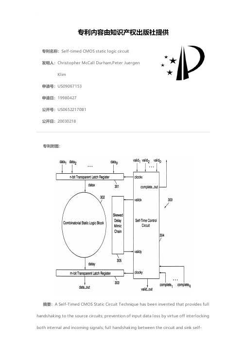
专利名称:Self-timed CMOS static logic circuit发明人:Christopher McCall Durham,Peter JuergenKlim申请号:US09067153申请日:19980427公开号:US06522170B1公开日:20030218专利内容由知识产权出版社提供专利附图:摘要:A Self-Timed CMOS Static Circuit Technique has been invented that provides full handshaking to the source circuits; prevention of input data loss by virtue off interlocking both internal and incoming signals; full handshaking between the circuit and sink self-timed circuitry; prevention of lost access operation information by virtue of an internal lock-out for the output data information; and plug-in compatibility for some classes of dynamic self-timed systems. The net result of the overall system is that static CMOS circuits can now be used to generate a self-timed system. This is in contrast to existing self-timed systems that rely on dynamic circuits. Thus, the qualities of the static circuitry can be preserved and utilized to their fullest advantage.申请人:INTERNATIONAL BUSINESS MACHINES CORPORATION代理机构:Winstead Sechrest & Minick P.C.代理人:Kelly K. Kordzik,Robert M. Carwell更多信息请下载全文后查看。
城市公共交通常用名词术语

城市公共交通常用名词术语一、基本术语1.1城市公共交通urban public transport城市中供公众乘用的、经济方便的各种交通方式的总称。
1.2公共交通方式public transport mode按公共交通工具类型划分的各种客运形式。
1.3城市公共交通系统urban public transport system由多种城市公共交通方式组成的有机总体。
1.4大运量客讼低?br> mass transit system城市公共交通中,运送大量乘客的有机总体。
1.5快速轨道交通rail rapid transit(RRT)通常以电能为动力,采取轮轨运黑心方式的快速大运量公共交通之总称。
1.6地下铁道,地铁subway由于城市中的一种速度快、运量大、行车间隔小的电动有轨客运系统,其部分线路设一地下隧道内。
1.7单轨运输系统monorail transit system车厢跨骑或悬持在架空的单轨上,由电力驱动的轨道客运系统。
1.8新交通系统new transport system新开发的具有高速、准点、舒适和污染小的交通方式及其运行服务系统的总体。
1.9垂直运送系统vertical transit system沿铅直方向运送乘客的有机整体。
1.10应急公共交通系统emergency public transport system在非常时期为应变而组成的临时公共交通系统。
1.11城市客渡urban ferry在城市区域及邻近郊县内,以运送乘客为主,横渡江河、湖泊的水上交通方式。
1.12索道缆车客运cableway transport在以架空钢索为轨道的线路上,以电能为动力由钢索牵引载客工具的运输方式。
1.13轨道缆车客运funicular railway transport在坡面铺设的轨道上,以电能为动力由钢索牵引载客工具的运输方式。
1.14公共交通信息系统public transport information system与公共交通服务有关的信号、数据、显示等所构成的有机整体。
防破解技术

防破解技术这里我们探讨一下可加强微控制器保护能力的技术。
如果某个项目能被分解成几部分,就可以把每部分放在不同的微控制器中。
那破解者就不得不对整个设备的所有部分进行反向工程。
但是,这种方法对于成本敏感的大批量产品来讲,不是个好方法。
从基于微控制器的设计转向 CPLD/FPGA 可能是个好的选择,因为破解 CPLD/FPGA 需要花费更多。
即使是将重要部分放在“不安全”的基于 SRAM 的 FPGA 中,其破解难度也相当大。
使用多层板和 BGA 封装也可以增大破解难度,因为肉眼无法看到内部互联,并且不可能直接访问 BGA 的引脚来进行分析。
为了能够访问引脚,芯片必须焊下来,放在特殊的测试适配器上。
这就需要特殊的工具和训练有素的工程师。
此外,BGA 的封装不同于 DIP SOIC 和QFP 之类,它的封装更难被打开。
常用的保护敏感信息的方法是加密数据。
但是,更应该需要关注密钥的存储和管理。
如果密钥是可编程的或能被随时修改,这非常类似于保存在 EEFPROM 中的情形。
把无格式的信息放在可编程的存储器中,对于系统的安全是个威胁。
半侵入式攻击和缺陷注入式攻击,给微控制器芯片的硬件安全带来巨大威胁,所以我们就研究一些方法来阻止这些攻击。
可以用自同步双线电路(Self-timed dual-rail circuit)设计技术,那样逻辑“1”或“0”不是被解码成在单线上的高或低电平,而是一对线上的‘HL’或‘LH’。
组合信号‘HH’会产生报警,导致处理器复位。
电路可以被设计成即使单个晶体管失效也不会导致安全问题。
这种技术会增加功耗分析攻击的难度。
当然,要平衡所需安全等级和保护技术的开销。
注:在使用 8031 的年代,不得不外扩 ROM/RAM。
当时有人使用到地址线/数据线的位交错技术,也就是某两位或更多的位线相互对掉。
这需要在画板子和写程序的时候同时使用。
1 不印字,重新印字和重新封装对付低级的攻击,业内广泛使用抹掉印字的方法,但它不能阻止信心坚定的对手。
外文翻译-D触发器

低功耗高效的D触发器电路摘要本文列举了低功耗高速率D触发器的设计。
它提出了各种技术,以尽量减少次临界漏电功率与CMOS电路的功耗。
本文提出的D触发器的一种设计以提高系统的整体速率,与其他电路相比。
这种技术可以让电路来实现最低功耗和最小的晶体管数量。
1.引言晶体管特征尺寸的缩放技术已经提供了一个在过去三十年中硅行业的显著的创新方法。
设计师们正努力使硅面积更小,更高速率,低功耗和可靠性,由于便携式电子产品的需求不断增加和普及。
动态功耗是数字系统的功耗主要因素之一。
为了减少动态功耗,已经取得了更小的几何尺寸,结果影响了静态功耗。
动态功耗与电源电压的平方成正比,因此显著降低电压以降低能耗。
器件尺寸的连续缩放,导致今天的超大规模集成电路的阈值电压显着增加,亚阈值漏电流成倍增长。
这大大增加了整体的总功耗。
在最近的纳米CMOS技术,如 90-、45-nm, 漏电流是几乎占了一半的总功耗这是并不少见。
在90nm节点,漏功率可高达35%的芯片功率。
由于便携式设备的使用和无线系统日益增强,减少这种功耗是非常必要的。
这些设备比单一的超大规模集成电路芯片的复杂得多。
他们有几个组成部分,可能是数字的或非数字的。
延长电池寿命为嵌入式应用,是在系统级完成的。
高功耗减少了电池使用寿命。
因此,电源最优化技术应适用于不同层次的数字化设计。
这些技术之一是使用低功耗的逻辑模式,这应该运用在逻辑锁存器和触发器的设计中。
2.简单文献回顾图1显示了单阈值传输门触发器。
D触发器采用CMOS传输门的构造如图2所示。
第一阶段(主), 由时钟信号驱动,而第二阶段(从)是由倒时钟信号驱动。
因此,主阶段是正电平感应而从阶段是负电平感应。
图1:单阈值传输门触发器图2:CMOS D型触发器的实现时钟为高电平时,D输入主传输门,而从传输门保持有以前的值。
当时钟, 从逻辑“1”变化到逻辑“0”时,主锁存器停止采样输入,存储在时钟过渡期间的D值。
在同一时间,从锁存器变得透明,传递存储的主Qm值到从传输门的输出。
- 1、下载文档前请自行甄别文档内容的完整性,平台不提供额外的编辑、内容补充、找答案等附加服务。
- 2、"仅部分预览"的文档,不可在线预览部分如存在完整性等问题,可反馈申请退款(可完整预览的文档不适用该条件!)。
- 3、如文档侵犯您的权益,请联系客服反馈,我们会尽快为您处理(人工客服工作时间:9:00-18:30)。
Single-Rail Self-timed Logic Circuits in Synchronous DesignsFrank Grassert, Dirk TimmermannUniversity of RostockInstitute for Applied Microelectronics and Computer ScienceRichard-Wagner-Str. 31, 18119 Rostock-Warnemünde, Germany{frank.grassert; dirk.timmermann}@etechnik.uni-rostock.deABSTRACTThis paper presents a self-timed scheme for dynamic single-raillogic integrated in a single phase clock design. A generalizedcompletion detection for generation of self-timed signals fromsingle-rail gates is described and we show a novel application ofthe redundancy of a SD-adder to ease the self-timed signalgeneration. Further we discuss an universal evaluation scheme toovercome the problem of only non-inverting functions withdynamic single-rail gates. The presented SD-adder wasintegrated in a synchronous scheme and combines theadvantages of simple synthesis and clock distribution forsynchronous designs with fastest evaluation. Self-timed schemesresult in fastest latch-free structures and robustness againstclock-skew. Further the single-rail scheme on gate-level yieldslower power consumption and smaller circuits. The use ofinverting and non-inverting single-rail gates makes the synthesis close to standard synthesis. Simulations for the redundant adder design show area and power savings of 40% and 30% compared to complementary DOMINO logic structure.1. INTRODUCTIONDynamic logic styles yield fast evaluation, high throughput and small latency. However, the main disadvantages are often multi-phase clocking schemes, dual-rail structures with large area and high power consumption. For highest speed, latch-free self-timed structures are used, which usually work with dual-rail logics. Single-rail logics are smaller and have less power consumption, but the generation of self-timed signals is difficult and only non-inverting functions can be used. Because the synthesis and clock distribution is much easier in synchronous designs a single phase clock is desirable and therefore, an integration of self-timed schemes in a synchronous structure combines fastest latch-free evaluation with single-clock behavior.DOMINO logic [1] is a simple realization of the dynamic idea but requires two clocking signals in minimum for pipelined designs (figure 1). For highest speed Harris et. al. [2] published a latch-free skew tolerant realization, where a scheme of overlapping clocking signals decreases sensitivity to clock slopes and the propagation delay is only the sum of the gate delays. Another disadvantage of DOMINO is, that only non-inverting logical functions can be realized. The clock-delayed DOMINO logic in [3] is an example of a single-rail dynamic logic, which uses dynamic nodes as inputs, but requires the detection of slowest inputs. In complex logic this requirement is hard to fulfill, because the evaluation time may depend on the input signals. Further, the problem of false discharge during precharging the inputs is not discussed. Other solutions for only non-inverting functions with DOMINO are avoiding all inverting functions in the netlist, but this often results in larger designs, or using a complementary structure (dual-rail). Here, for each signal an inverted signal exists.A different approach for highest speed is the use of dynamic logic styles in asynchronous designs [4]. In [5], a divider using a ring structure was realized and yields no delay in addition to the evaluation time. Such self-timed techniques require completion signals and, therefore, differential logic styles or dual-rail realizations are used. In [6], Differential Cascode Voltage Switch Logic (DCVSL) was introduced (figure 1). It builds the starting point for several differential logic styles and was derived from two complementary DOMINO gates with merged logic trees.In this paper,• the main goal is the usage of short self-timed chains in synchronous designs for fast latch-free evaluation.• the presented generalized completion detection makes the usage of single-rail logic in self-timed schemes possible. • the novel application of the redundancy of a SD-adder eases the self-timed signal generation.• the presented evaluation scheme allows the use of dynamic nodes as inputs and we overcome the problem of only non-inverting outputs for dynamic single-rail logics.• the simulated adder combines synchronous behavior with small latency and low power consumption.Section 2 describes the basics of self-timed structures and the completion detection in single-rail dynamic logic. A possibility to use dynamic nodes as direct inputs is introduced in section 3. In section 4 the design of an asynchronous redundant adder is explained and the results are discussed in section 5. Section 6 presents the conclusions.n-logic n-logicinverter inverter inverterDOMINO DCVSFigure 1. DOMINO, and DCVS logic; DCVSL mergesthe complementary logic function in the n-block;DOMINO and DCVS need more than one clock signalin pipelined structures2. SELF-TIMED STRUCTURES2.1 BasicsIn a differential logic style the complementary functions are merged together and are not independent. This sometimes results in less transistors and, therefore, in a smaller area in comparison with dual-rail DOMINO logic. In contrast any single-rail logic can be converted to dual-rail logic by independently building the complementary logic part.Differential logic styles are used for self-timed circuits where we need to detect whether a gate has evaluated. In dynamic logic styles both complementary output signals have the same value during precharge, but change to different values during evaluation. Therefore, the generation of completion signals is simple. This seems to be an advantage, but we have to reflect that this results from the overhead of complementary signals. Therefore, a dual-rail structure becomes more efficient in self-timed circuits.2.2 Self-timed SchemesSelf-timed structures reduce the latency and make latches and flipflops unnecessary. In [7] we presented a scheme to include self-timed structures in a global clock system. There it is possible, that the critical path has an evaluation time of only the sum of all the evaluation times of the single gates without additional delays through latches. Therefore, the evaluation time of the critical path is the minimum clock period. However, the structure must be carefully designed and a calculation of the timing behavior is advantageous. Furthermore, such structure reduces the sensibility against clock skew and, consequently, no additional delays for a safe function is necessary.There are two main ways to build up a self-timed scheme for dynamic logic: the gate outputs control the clocking of the previous or the following gate. The main advantage of the first structure is a simple implementation with minimum evaluation time. If the evaluated outputs of a gate have settled, a completion signal is generated and this sets the previous gate in the precharge phase (inputs are processed – start precharge). Precharged outputs set the previous gate in the evaluation phase (outputs are precharged – start next evaluation, inputs can be processed). Because the evaluation of the outputs starts only with valid inputs, every gate is waiting for valid inputs during the evaluation phase. Therefore, the evaluation time is only the sum of the gate evaluation times with no additional delays. Figure 2 shows such a dynamic dual-rail self-timed structure.2.3 Generalized Completion DetectionThe completion detection follows the principle of differentiating the states of the outputs nodes after precharge and after evaluation. A complementary structure ensures an output change on every gate, because the complementary outputs are generated independently. To generalize this behavior we can detect the completion on a set of n output signals of n different gates, if they fulfill the equation:f1(Im) or f2(Imà ÃÃà Ãsn(Im) = 1.This assumes that all these gates fievaluate in a small range oftime, so that completion generation does not disturb slower orfaster paths. This assumption seems reasonable in most smallblocks with limited logic depth, for example in data paths. Then,during precharge all outputs stay on the same value and duringevaluation at least one output must change its value and,therefore, the completion detection is ensured. The completionlogic is little enlarged because a 3- or more-input NOR can benecessary. The essential gate outputs can be find out by logicsynthesis. If no such completion can be applied, an additionalgate must be implemented exclusive for self-timed generation.The utilization of a redundant number system is a good way foreasy completion generation (section 4).3. SINGLE-RAIL LOGICThe main goal for the use of dynamic logic styles is to use onlyfaster n-transistors in the logic trees, to achieve higherperformance and smaller area. The problem of directlyconnecting two dynamic stages is, that the precharged highoutput node will result in conducting n-transistors in thefollowing logic tree. At the beginning of the evaluation phasethis connection to ground can lead to a discharge of thefollowing output and in an erroneous state. DOMINO logicsolves this issue with an inverter, so following n-transistors areoff and no discharge can occur. Therefore, single-rail logic styleslike DOMINO can realize only non-inverting functions. Toovercome these limitation the following conditions for evaluationand precharge must be hold.3.1 Generalized Conditions for EvaluationTo use simple single-rail logic equivalent to static CMOS aninversion is necessary. For the following explanations we definea DOMINO output (dynamic stage plus inverter) as a non-inverted signal and the dynamic node (output of the dynamicstage) as the inverted signal. It may be allowed to directlyconnect two consecutive dynamic stages with the inverted signal(without the inverter of DOMINO), if it is ensured thata) at least one series transistor exists, which is connected to anon-inverted (DOMINO) output (with position next to thedynamic node to prevent charge sharing) andb) the non-inverted input signals arrive later than the invertedinput signals.In this case at least one transistor disjoins the output from theground during the precharge phase and at the beginning of theevaluation. When the inverted outputs arrive first, they havesufficient time to switch off all n-transistors. The non-inverted(DOMINO) outputs arrive later and all other transistors areFigure 2. Self-timed structure with dual-rail dynamiclogicalready in their correct evaluation state and no erroneous discharging can appear. To force this function a dimensioning of the gates or a delaying of the non-inverted outputs is possible. Figure 3 shows this behavior. Input A is a non-inverted input and arrives with one inverter delay compared to input B and C. This results in a limited logic function of a gate. Figure 3 shows the resulting structure of the n-logic trees. No OR-gate is possible with at least one inverted input. However, in dynamic logic an OR-gate should be in any case implemented as a parallel path in the previous logic block, because only parallel transistors are necessary and these do not delay the evaluation. Further, AND-functions with only inverted inputs are not allowed, but this can be transformed to a NOR-function with non-inverted inputs (OR-function, where the inverted output is used).It should be noted, that the logic style is not fixed to DOMINO logic. All dynamic logics are feasible including adapted differential styles, where the logic trees of two or more independent functions are merged.3.2 Conditions for PrechargeAs illustrated in figure 3 (dotted lines in timing diagram) an erroneous discharge can occur if the input signals are precharged during evaluation and the gate has not discharged the internal dynamic node. During precharge the inverted outputs settle to the high value first. Later the non-inverted (DOMINO) outputs settle to low value delayed by the inverter. Therefore, a path to ground can exist for a short time if all inverted nodes are already precharged but the non-inverted (DOMINO) output has not. If necessary, this problem can be solved through disconnecting the logic tree from ground, if the evaluation has finished.3.3 Operation in Self-timed CircuitsFor our self-timed structure we can solve the problem of false discharge during precharging the inputs in a simple way. Aftercompletion detection the previous gates are set to precharge. This signal can be used to disconnect the own logic-tree from ground. Then, both clock transistors in the dynamic gate are controlled separately. The n-transistor is clocked with the own completion signal, the p-transistor is controlled from the self-timed signal of the following stage. Figure 4 shows such a modified structure. Consequently, no valid inputs are allowed during precharge phase to prevent a short circuit. If this can not be guaranteed the separate use of the clock transistors is not possible and an additional n-transistor is necessary for disconnecting the logic-tree after evaluation. It should be noted, that such modifications depend on the timing behavior and they are not always necessary.3.4 Integration in a Global Clock SchemeAn integration of the presented single-rail scheme in a synchronous single phase clock design targets a simpler synthesis, clock distribution and usage. In [7] we presented a scheme to integrate self-timed schemes in a true single phase clock scheme. The main ideas are to use short chains of asynchronous logic to keep runtime differences negligible and to clock the last gate of such a chain with the global clock.During synchronization of the single-rail self-timed logic to the global clock it has to be ensured that the precharge conditions are not broken and that the information can be stored before the last gate. Here, an additional serial n-clock-transistor in the logic tree of the global clocked gate is necessary to ensure the function. One n-clock-transistor is controlled by the global clock, the second one is controlled with the own completion signal. Therefore, the second transistor prevents a false discharge, if the input values precharge during evaluation and the first transistor prevents a short circuit during precharge with valid inputs.4. SINGLE -RAIL SELF -TIMED SD -ADDERAs an example implementation of the presented ideas a redundant signed digit (SD) adder is used. The redundant digits –1, 0, 1 are represented with two signals, e.g. two bit. To simplify the completion detection the digit representation shown in table 1 is used. This scheme ensures that at least one signal changes its value during evaluation. Therefore, the generalized completion detection is simple to implement. For testing purposes blocks of one bit adders were implemented. These adders generate the carry free redundant result in three stages of dynamic logic. Self-timed signals are generated for each stage, therefore, one adder contains a chain of three stages (figure 5) of DOMINO logic.n-logic inverterinverterA φAB C!Q QFigure 3. Structure of single-rail DOMINO and timing diagram (all negative inputs must arrive first; the timing diagram also shows the problem of false discharge during precharging the inputs) and essential structure of a single-rail DOMINO n-block; the AND-function with a non-inverted input prevents a prematurely dischargeFigure 4. New modified self-timed scheme for single-rail dynamic logic; the self-timed signals were generated from the outputs of several gatesN ...Then, we combined these two bit adders to a larger adder structure with consecutive blocks (a + b) + (c + d). This results in a self-timed chain of six stages. This structure was synchronized to a global clock with a modified AC-TSPC scheme presented in [7] (figure 5).Table 1. SD-digit representationDigit Self-timed representation -1 10 0 011 11free 00 – prechargeThe timing differences between parallel paths must be small.Therefore, short chains are meaningful and simpler to realize. Anintensive timing calculation can predict the timing behavior.Then, critical paths can be adapted for reliable function.5. RESULTS The simulations were done for a 0.6 µm AMS process at 3.3V.Figure 6 shows our results in terms of power, area and speed in comparison to the same structure in complementary DOMINO logic.An initialization period is crucial for simulating the self-timed structure. During switch-on an internal state can occur where more than one valid signals remain in the self-timed pipe. The starting point can be reached by clocking the pipeline without valid inputs. Then an ‘empty’ state can be achieved where the self-timed structure is reset.The comparison shows that the area is reduced to 58%. Thesimple complementary DOMINO logic always needs two complementary signals. The self-timed structure requires additional logic for completion detection (11%). However, because of the higher clock load of the DOMINO structure (476 transistors) the self-timed structure saves also area in the clock tree (only 12 transistors).The reduction in area results in a reduction in the power consumption. In complementary DOMINO logic one node is continuously discharged. The power consumption has been reduced to 70%. In self-timed logic we have additional power consumption due to the completion detection but lower power in the clock tree.The speed of the DOMINO structure is slightly slower because of the higher loads of the dual-rail structure. Until now the simulated structures have not been optimized. Most transistors were sized to 7 for p-devices and 4 for n-devices.6. CONCLUSIONSThis paper presents a realization of a dynamic single-rail self-timed logic integrated in a synchronous clock. Three mainproblems were solved: generating self-timed signals in single-rail logic, realizing inverting and non-inverting functions in dynamicsingle-rail logic and synchronizing short chains of self-timed gates. Additionally, the utilization of the redundancy of a SD-adder eased the self-timed generation in our example realization. The redundant number adder structure was simulated and showsthe possibility of realizing single-rail self-timed circuits indynamic logic. The self-timed structure ensures, that all signalsmeet the determined conditions and this results in a fast latch-free evaluation for a synchronous design. In comparison to a DOMINO realization the power and area consumption wasreduced to about 70% and 60%, respectively. 7. REFERENCES[1] R. H. Krambeck, C. M. Lee and H.-F. S. Law, “High-SpeedCompact Circuits with CMOS”, Journal of Solid-State Circuits, IEEE, Vol. SC-17, No. 3, Jun. 1982.[2] D. Harris and M. A. Horowitz, “Skew-Tolerant DominoCircuits”, Journal of Solid-State Circuits, IEEE, Vol. 32, No. 11, Nov. 1997.[3] G. Yee, C. Sechen, “Clock-Delayed Domino for DynamicCircuit Design”, IEEE Transactions on VLSI Systems, Vol. 8, No. 4 , Aug. 2000.[4] G. M. Jacobs, R. W. Brodersen, “A Fully AsynchronousDigital Signal Processor Using Self-timed Circuits”, Journal of Solid-State Circuits, IEEE, Vol. 25, No. 6, Dec. 1990. [5] T. E. Williams and M. A. Horowitz, “A Zero-OverheadSelf-Timed 160-ns 54-b CMOS Divider”, Journal of Solid-State Circuits, IEEE, Vol. 26, No. 11, Nov. 1991.[6] L. G. Heller, W. R. Griffin, J. W. Davis and N. G. Thoma,“Cascode Voltage Switch Logic: A Differential CMOS Logic Family”, Proceedings of International Solid-State Circuits Conference, IEEE, 1984, pp. 16-17.[7] F. Grassert, D. Timmermann, “Dynamic Single Phase Logicwith Self-timed Stages for Power Reduction in Pipeline Circuit Designs”, International Symposium on Circuits and Systems (ISCAS), IEEE, May 2001, pp. IV 144-147.Figure 5. Structure of the self-timed SD-adder; a 1 bit cell consists of three dynamic single-rail stagesPower (µW/MHz)Max. delay (ns)DOMINOFigure 6.。