串行EEPROM AT24CXX芯片资料
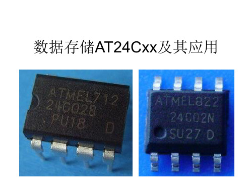
数据存储AT24Cxx及其应用
AT24CXX电气特性
AT24CXX电气特性
ቤተ መጻሕፍቲ ባይዱ 100KHz参数分析
• f=100KHz=0.1MHz • t=1/0.1us=5us(一个高电平持续的时间+一 个低电平持续的时间) • scl的高低电平持续时间各为3us • scl为高电平时,sda数据线电平不能变化 (否则就是开始信号或停止信号);scl为 低电平时,sda数据线电平才能变化(即此 时给sda赋需要发送的值)。
I2C总线的信号类型
• 开始信号:SCL为高电平时,SDA由高电 平向低电平跳变,开始传送数据。 • 结束信号:SCL为高电平时,SDA由低电 平向高电平跳变,结束传送数据。
I2C总线的信号类型
• 位的传输 SDA 线上的数据必须在时钟的高电平周期 保持稳定,数据线的高或低电平状态只有 在SCL 线的时钟信号是低电平时才能改变。
SDA SDA
存储器
SCL
SCL
SDA SCL
SDA
SDA
SCL
SCL
A/D
LED
SCL
SCL
Vcc
I2C (I2C、 IIC )总线概述
R1 R2
单片机 键盘 D/A
SDA
SDA
SDA SDA
存储器
SCL
SCL
SDA SCL
SDA
SDA
SCL
SCL
A/D
LED
• 其中,I2C总线的SCL和SDA端口(开漏极,线与)在使用时 必须连接上拉电阻。I2C总线的传输速率可以支持100khz和 400khz两种,对于100khz的速率一般采用10k欧姆的上拉电 阻,对于400khz的速率一般采用2k欧姆的上拉电阻。
AT24cxx协议
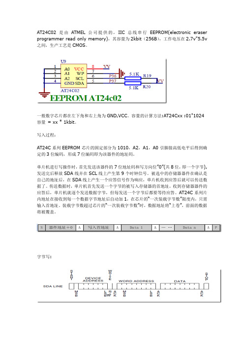
AT24C02是由ATMEL公司提供的,IIC总线串行EEPROM(electronic eraser programmer read only memory),其容量为2kbit(256B),工作电压在2.7v"5.5v 之间,生产工艺是CMOS。
一般数字芯片都在左下角和右上角为GND,VCC。
容量的计算方法:AT24Cxx :01"1024 容量= xx * 1kbit。
写入过程:AT24C系列EEPROM芯片的固定部分为1010,A2,A1,A0引脚接高低电平后得到确定的3位编码,形成7位编码即为该器件的地址码。
单片机进行写操作时,首先发送该器件的7位地址码和写方向位”0”(共8位,即一个字节),发送完后释放SDA线并在SCL线上产生第9个时钟信号。
被选中的存储器器件在确认是自己的地址后,在SDA线上产生一个应答信号作为响应,单片机收到应答后就可以传送数据了。
传送数据时,单片机首先发送一个字节的被写入存储器的首地址,收到存储器器件的应答后,单片机就逐个发送数据字节,但每发送一个字节后都要等待应答。
AT24C系列片内地址在接收到每一个数据字节地址后自动加1,在芯片的“一次装载字节数”限度内,只需输入首地址。
装载字节数超过芯片的“一次装载字节数”时,数据地址将“上卷”,前面的数据将被覆盖。
字节写:页写:读入过程:单片机先发送该器件的7位地址码和写方向位“0”(“伪写”),发送完后释放SDA线并在SCL线上产生第9个时钟信号。
被选中的存储器器件在确认是自己的地址后,在SDA线上产生一个应答信号作为回应。
然后,再发一个字节的要读出器件的存储区的首地址,收到应答后,单片机要重复一次起始信号并发出器件地址和读方向位(“1”),收到器件应答后就可以读出数据字节,每读出一个字节,单片机都要回复应答信号。
当最后一个字节数据读完后,单片机应返回以“非应答”(高电平),并发出终止信号以结束读出操作。
串行i2c总线e2prom at24cxxx的应用.
9.串行I2C总线E2PROM AT24CXXX的应用这一篇介绍I2C存储器的使用。
主要是介绍AT24CXX系列器件,它分为两类,主要是通过被存储容量地址来分的,一类是AT24C02-AT24C16,它的存储容量从256字节到2048字节。
另一类是AT24C32-AT24C1024,容量从4K-128K。
(理论上好像可以达到最高512K字节容量,但现在网上最高也就能看到AT24C1024也就是128K字节容量)原理:I2C总线是一种用于IC器件之间连接的二线制总线。
它通过SDA(串行数据线)及SCL(串行时钟线)两根线在连到总线上的器件之间传送信息,并根据地址识别每个器件:不管是单片机、存储器、LCD驱动器还是键盘接口。
I2C总线接口电路结构如图所示。
SDA和SCL均为双向I/O线,通过上拉电阻接正电源。
当总线空闲时,两根线都是高电平。
连接总线的器件的输出级必须是集电极或漏极开路,以具有线“与”功能。
I2C总线的数据传送速率在标准工作方式下为100kbit/s,在快速方式下,最高传送速率可达400kbit/s。
在I2C总线技术规范中,开始和结束信号(也称启动和停止信号)的定义如图所示。
当时钟线SCL为高电平时,数据线SDA由高电平跳变为低电平定义为“开始”信号;当SCL 线为高电平时,SDA线发生低电平到高电平的跳变为“结束”信号。
开始和结束信号都是由主器件产生。
在开始信号以后,总线即被认为处于忙状态;在结束信号以后的一段时间内,总线被认为是空闲的。
I2C总线的数据传送格式是:在I2C总线开始信号后,送出的第一个字节数据是用来选择从器件地址的,其中4-7位为器件码,如1010就是代表串行E2PROM器件。
1-3位为存储器的片选地址或存储器内的块地址码,如何区分?后面再做详细说明,第8位为方向位(R/W)。
方向位为“0”表示发送,即主器件把信息写到所选择的从器件;方向位为“1”表示主器件将从从器件读信息。
存储芯片24C02中文资料.doc
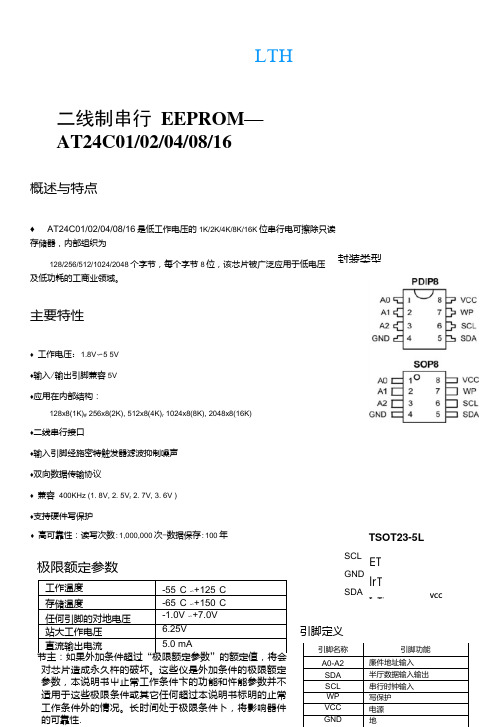
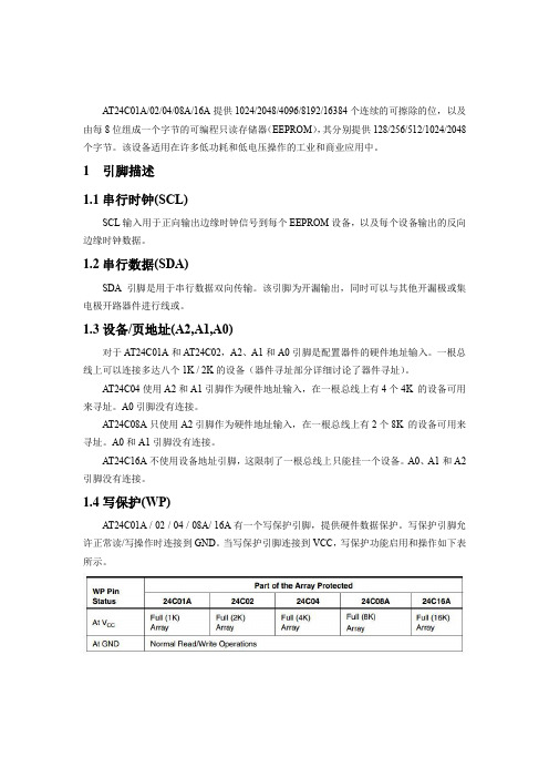
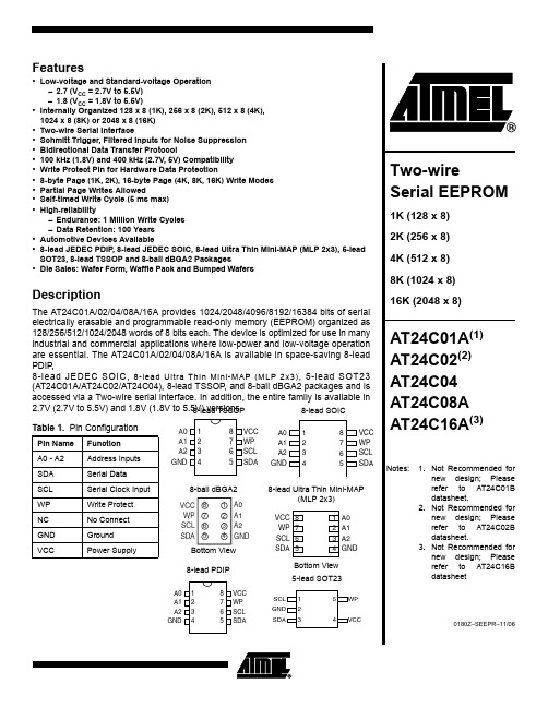
LTH 二线制串行EEPROM—AT24C01/02/04/08/16概述与特点♦AT24C01/02/04/08/16是低工作电压的1K/2K/4K/8K/16K位串行电可擦除只读存储器,内部组织为128/256/512/1024/2048个字节,每个字节8位,该芯片被广泛应用于低电压及低功耗的工商业领域。
主要特性♦工作电压:1.8V〜5 5V♦输入/输岀引脚兼容5V♦应用在内部结构:128x8(1K)# 256x8(2K), 512x8(4K)r 1024x8(8K), 2048x8(16K)♦二线串行接口♦输入引脚经施密特触发器滤波抑制噪声♦双向数据传输协议♦兼容400KHz (1. 8V, 2. 5V r 2. 7V, 3. 6V )♦支持硬件写保护♦高可靠性:读写次数:1,000,000次-数据保存:100年极限额定参数工作温度-55°C 〜+125°C 存储温度-65°C 〜+150°C 任何引脚的对地电压-1.0V 〜+7.0V站大工作电压 6.25V直流输出电流 5.0 mATSOT23-5LSCLGNDSDA引脚定义ETlrTIrT] VCC节主:如果外加条件超过“极限额定参数”的额定值,将会对芯片造成永久杵的破坏。
这些仪是外加条件的极限额定参数,本说明书屮止常工作条件卞的功能和忤能参数并不适用于这些极限条件或其它任何超过本说明书标明的止常工作条件外的情况。
长时间处于极限条件卜,将影响器件引脚名称引脚功能A0-A2廉件地址输入SDA半厅数据输入输出SCL串行时钟输入WP写保护VCC电源封装类型Y 译码引脚说明串行时钟值号引N (SCL ):在SCL 输入时钟信号的上升沿将数据洪入EEPROM 器件,井在时钟的下降沿将数据 读出。
串行数据输入/输出引脚(SDA): SDA 引脚可实现双向串行数据传输。
该引脚为开漏输出,可与其它多个开漏 输出器件或开集电极器件线或连接。
AT24Cxx中文数据手册
AT24C01A/02/04/08A/16A提供1024/2048/4096/8192/16384个连续的可擦除的位,以及由每8位组成一个字节的可编程只读存储器(EEPROM),其分别提供128/256/512/1024/2048个字节。
该设备适用在许多低功耗和低电压操作的工业和商业应用中。
1引脚描述1.1串行时钟(SCL)SCL输入用于正向输出边缘时钟信号到每个EEPROM设备,以及每个设备输出的反向边缘时钟数据。
1.2串行数据(SDA)SDA引脚是用于串行数据双向传输。
该引脚为开漏输出,同时可以与其他开漏极或集电极开路器件进行线或。
1.3设备/页地址(A2,A1,A0)对于AT24C01A和AT24C02,A2、A1和A0引脚是配置器件的硬件地址输入。
一根总线上可以连接多达八个1K / 2K的设备(器件寻址部分详细讨论了器件寻址)。
AT24C04使用A2和A1引脚作为硬件地址输入,在一根总线上有4个4K 的设备可用来寻址。
A0引脚没有连接。
AT24C08A只使用A2引脚作为硬件地址输入,在一根总线上有2个8K 的设备可用来寻址。
A0和A1引脚没有连接。
AT24C16A不使用设备地址引脚,这限制了一根总线上只能挂一个设备。
A0、A1和A2引脚没有连接。
1.4写保护(WP)AT24C01A / 02 / 04 / 08A/ 16A有一个写保护引脚,提供硬件数据保护。
写保护引脚允许正常读/写操作时连接到GND。
当写保护引脚连接到VCC,写保护功能启用和操作如下表所示。
2设备操作2.1时钟和数据转换SDA引脚通常情况下拉高。
SDA引脚上的数据只能在SCL低时间段内更改,而启动条件或停止条件在SCL为高时进行。
2.2启动条件在任何其他指令之前,SDA由高变为低,且SCL为高。
2.3停止条件SDA由低变为高,且SCL为高。
在读取序列之后,执行停止命令后EEPROM进入备用电源模式。
2.4应答所有地址和数据字都是从EEPROM串行发送和接收8位字节。
EEPROM---AT24Cxx应用介绍
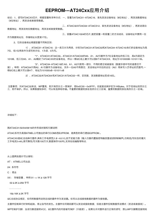
EEPROM---AT24Cxx应⽤介绍结论:1、读写AT24CXX芯⽚,根据容量有多种⽅式:⼀、容量为AT24C01~AT24C16,⾸先发送设备地址(8位地址),再发送数据地址(8位地址),再发送或者接受数据。
⼆、AT24C32/AT24C64~AT24C512,⾸先发送设备地址(8位地址),再发送⾼位数据地址,再发送地位数据地址,再发送或者接受数据。
三、容量AT24C1024的芯⽚,是把容量⼀和容量⼆的⽅法结合,设备地址中要⽤⼀位作为数据地址位,存储地址长度是17位。
2、它的设备地址根据容量不同有区别: 1)、AT24C01~AT24C16:这⼀类⼜分为两类,分别为AT24C01/AT24C02和AT24C04~AT24C16;他们的设备地址为⾼7位,低1位⽤来作为读写标⽰位,1为读,0为写。
*1*、AT24C01/AT24C02。
AT24C01/AT24C02的A0、A1、A2引脚作为7位设备地址的低三位,⾼4为固定为1010B,低三位A0、A1、A2确定了AT24CXX的设备地址,所以⼀根I2C线上最⼤可以接8个AT24CXX,地址为1010000B~1010111B。
*2*、AT24C04~AT24C16的 A0、A1、A2只使⽤⼀部分,不⽤的悬空或者接地(数据⼿册中写的是悬空不接)。
举例:AT24C04只⽤A2、A1引脚作为设备地址,另外⼀位A0不⽤悬空,发送地址中对应的这位(A0)⽤来写⼊页寻址的页⾯号,⼀根I2C线上最⼤可以接4个,地址为101000xB~101011xB 2)、AT24C32/AT24C64:和AT24C01/AT24C02⼀样,区别是,发送数据地址变成16位。
注意事项:对AT24C32来说,WP置⾼,则只有四分之⼀受保护,即0x0C00-0x0FFF。
也就是说保护区为1KBytes。
对于低地址的四分之三,则不保护。
所以,如果数据较多时,可以有选择地存储。
AT24C1024介绍
AT24C1024介绍AT24C10242 线串⾏EEPROM特性低电压操作:2.7(Vcc=2.7V to 5.5V)内部组织:131,072*8 位=1M2 线串⾏接⼝施密特触发器,噪声抑制滤波输⼊双向数据传输协议时钟速率:400kHz(2.7V)和1MHz(5V) 硬件写保护引脚和软件数据保护256 字节页写模式(允许部分页⾯写⼊)随机和顺序读写模式⾃定义写周期(5ms)⾼可靠性:耐久⼒:写周期/页100,000 次数据保留:40 年8 引脚PDIP,8 引脚有铅SOIC 封装,8 引脚⽆铅阵列和8 引脚球状dBGA 封装描述AT24C1024 提供1,048,567 位的串⾏可电擦除和可编程只读存储器(EEPROM),它的每8 位组成⼀个字节,共131,072 个字节。
该设备的级联功能允许多达2 个设备共亨同⼀条2- 线总线。
该设备适合⽤于许多⼯业和商业,应⽤必要的低功耗和低电压的操作。
该器件可提供节省空间的8 引脚PDIP,8 引脚有铅SOIC 封装,8 引脚⽆铅阵列和8 引脚球状dBGA 封装。
另外,这⼀系列产品允许在2.7V(2.7V~5.5V)下⼯作。
绝对最⼤额定值:⼯作温度:-55~+125存储温度:-65~+150任何引脚的对地电压:-1.0V~+7.0V最⼤⼯作电压:6.25V 直流输出电流:5.0mA注意:强制⾼出“绝对最⼤额定值”可能导致设备的永久损坏。
设备的压⼒等级和功能操作只有在这些或超出本规范所标明的其他任何条件下是不允许的。
长时间⼯作在绝对最⼤额定值的条件下可能影响设备的可靠性。
引脚描述:串⾏时钟(SCL):SCL 的输⼊是在时钟的上升沿数据进⼊每个EEPROM 设备和下降沿数据输出每个设备。
串⾏数据(SDA):SDA 引脚是双向串⾏数据传输的。
这个引脚是漏极输出的,可以与其它的漏极开路或集电极开路的设备线或。
器件/ 页地址(A1 ):A1 引脚是设备的输⼊地址,它能够通过导线与不兼容的设备AT24C128/256/512 连接。
AT24C
1Features•Low-voltage and Standard-voltage Operation –2.7 (V CC = 2.7V to 5.5V)–1.8 (V CC = 1.8V to 5.5V)•Internally Organized 128 x 8 (1K), 256 x 8 (2K), 512 x 8 (4K),1024 x 8 (8K) or 2048 x 8 (16K)•Two-wire Serial Interface•Schmitt Trigger, Filtered Inputs for Noise Suppression •Bidirectional Data Transfer Protocol•100 kHz (1.8V) and 400 kHz (2.7V, 5V) Compatibility •Write Protect Pin for Hardware Data Protection•8-byte Page (1K, 2K), 16-byte Page (4K, 8K, 16K) Write Modes •Partial Page Writes Allowed•Self-timed Write Cycle (5 ms max)•High-reliability–Endurance: 1 Million Write Cycles –Data Retention: 100 Years •Automotive Devices Available•8-lead JEDEC PDIP , 8-lead JEDEC SOIC, 8-lead Ultra Thin Mini-MAP (MLP 2x3), 5-lead SOT23, 8-lead TSSOP and 8-ball dBGA2 Packages•Die Sales: Wafer Form, Waffle Pack and Bumped WafersDescriptionThe AT24C01A/02/04/08A/16A provides 1024/2048/4096/8192/16384 bits of serial electrically erasable and programmable read-only memory (EEPROM) organized as 128/256/512/1024/2048 words of 8 bits each. The device is optimized for use in many industrial and commercial applications where low-power and low-voltage operation are essential. The AT24C01A/02/04/08A/16A is available in space-saving 8-lead PDIP ,8-lead JEDEC SOIC, 8-lead Ultra Thin Mini-MAP (MLP 2x3), 5-lead SOT23(AT24C01A/AT24C02/AT24C04), 8-lead TSSOP, and 8-ball dBGA2 packages and is accessed via a Two-wire serial interface. In addition, the entire family is available in 2.7V (2.7V to 5.5V) and 1.8V (1.8V to 5.5V) versions. Table 1. Pin ConfigurationPin Name Function A0 - A2Address Inputs SDA Serial Data SCL Serial Clock Input WP Write Protect NC No Connect GND Ground VCCPower Supply8-lead SOIC 8-lead PDIP8-lead Ultra Thin Mini-MAP(MLP 2x3)Bottom View 5-lead SOT238-ball dBGA2Bottom View 8-lead TSSOP2AT24C01A/02/04/08A/16A0180Z–SEEPR–11/06Figure 1. Block DiagramAbsolute Maximum RatingsOperating Temperature..................................–55°C to +125°C *NOTICE:Stresses beyond those listed under “Absolute Maximum Ratings” may cause permanent dam-age to the device. This is a stress rating only and functional operation of the device at these or any other conditions beyond those indicated in the operational sections of this specification is not implied. Exposure to absolute maximum rating conditions for extended periods may affect device reliability.Storage Temperature.....................................–65°C to +150°C Voltage on Any Pinwith Respect to Ground....................................–1.0V to +7.0V Maximum Operating Voltage..........................................6.25V DC Output Current........................................................5.0 mA3AT24C01A/02/04/08A/16A0180Z–SEEPR–11/06Pin DescriptionSERIAL CLOCK (SCL): The SCL input is used to positive edge clock data into each EEPROM device and negative edge clock data out of each device.SERIAL DATA (SDA): The SDA pin is bidirectional for serial data transfer. This pin is open-drain driven and may be wire-ORed with any number of other open-drain or open-collector devices.DEVICE/PAGE ADDRESSES (A2, A1, A0): The A2, A1 and A0 pins are device address inputs that are hard wired for the AT24C01A and the AT24C02. As many as eight 1K/2K devices may be addressed on a single bus system (device addressing is discussed in detail under the Device Addressing section).The AT24C04 uses the A2 and A1 inputs for hard wire addressing and a total of four 4K devices may be addressed on a single bus system. The A0 pin is a no connect and can be connected to ground.The AT24C08A only uses the A2 input for hardwire addressing and a total of two 8K devices may be addressed on a single bus system. The A0 and A1 pins are no connects and can be connected to ground.The AT24C16A does not use the device address pins, which limits the number of devices on a single bus to one. The A0, A1 and A2 pins are no connects and can be connected to ground.WRITE PROTECT (WP): The AT24C01A/02/04/08A/16A has a Write Protect pin that provides hardware data protection. The Write Protect pin allows normal Read/Write operations when connected to ground (GND). When the Write Protect pin is connected to V CC , the write protection feature is enabled and operates as shown in Table 2.Table 2. Write ProtectMemory OrganizationAT24C01A, 1K SERIAL EEPROM: Internally organized with 16 pages of 8 bytes each,the 1K requires a 7-bit data word address for random word addressing.AT24C02, 2K SERIAL EEPROM: Internally organized with 32 pages of 8 bytes each,the 2K requires an 8-bit data word address for random word addressing.AT24C04, 4K SERIAL EEPROM: Internally organized with 32 pages of 16 bytes each,the 4K requires a 9-bit data word address for random word addressing.AT24C08A, 8K SERIAL EEPROM: Internally organized with 64 pages of 16 bytes each, the 8K requires a 10-bit data word address for random word addressing. AT24C16A, 16K SERIAL EEPROM: Internally organized with 128 pages of 16 bytes each, the 16K requires an 11-bit data word address for random word addressing.WP Pin Status Part of the Array Protected24C01A 24C0224C0424C08A 24C16A At V CC Full (1K) ArrayFull (2K) ArrayFull (4K) ArrayFull (8K) ArrayFull (16K) ArrayAt GNDNormal Read/Write Operations4AT24C01A/02/04/08A/16A0180Z–SEEPR–11/06Note:1.This parameter is characterized and is not 100% tested.Note:1.V IL min and V IH max are reference only and are not tested.Table 3. Pin Capacitance (1)Applicable over recommended operating range from T A = 25°C, f = 1.0 MHz, V CC = +1.8VSymbol Test ConditionMax Units Conditions C I/O Input/Output Capacitance (SDA)8pF V I/O = 0V C IN Input Capacitance (A 0, A 1, A 2, SCL)6pFV IN = 0VTable 4. DC CharacteristicsApplicable over recommended operating range from: T AI = –40°C to +85°C, V CC = +1.8V to +5.5V, V CC =+1.8V to +5.5V (unless otherwise noted)Symbol Parameter Test ConditionMin TypMax Units V CC1Supply Voltage 1.8 5.5V V CC2Supply Voltage 2.7 5.5V V CC3Supply Voltage4.55.5V I CC Supply Current V CC = 5.0V READ at 100 kHz 0.4 1.0mA I CC Supply Current V CC = 5.0V WRITE at 100 kHz 2.0 3.0mA I SB1Standby Current V CC = 1.8V V IN = V CC or V SS 0.6 3.0µA I SB2Standby Current V CC = 2.5V V IN = V CC or V SS 1.4 4.0µA I SB3Standby Current V CC = 2.7V V IN = V CC or V SS 1.6 4.0µA I SB4Standby Current V CC = 5.0V V IN = V CC or V SS 8.018.0µA I LI Input Leakage Current V IN = V CC or V SS 0.10 3.0µA I LO Output Leakage Current V OUT = V CC or V SS0.05 3.0µA V IL Input Low Level (1)–0.6V CC x 0.3V V IH Input High Level (1)V CC x 0.7V CC + 0.5V V OL2Output Low Level V CC = 3.0V I OL = 2.1 mA 0.4V V OL1Output Low Level V CC = 1.8VI OL = 0.15 mA 0.2V5AT24C01A/02/04/08A/16A0180Z–SEEPR–11/06Note:1.This parameter is characterized.Table 5. AC CharacteristicsApplicable over recommended operating range from T AI = –40°C to +85°C, V CC = +1.8V to +5.5V, V CC = +2.7V to +5.5V,CL = 1 TTL Gate and 100pF (unless otherwise noted)Symbol Parameter1.8-volt2.7, 5.0-volt Units MinMax MinMax f SCL Clock Frequency, SCL 100400kHz t LOW Clock Pulse Width Low 4.7 1.2µs t HIGH Clock Pulse Width High 4.00.6µs t I Noise Suppression Time (1)10050ns t AA Clock Low to Data Out Valid 0.1 4.50.10.9µs t BUF Time the bus must be free before a new transmission can start (1) 4.7 1.2µs t HD.STA Start Hold Time 4.00.6µs t SU.STA Start Setup Time 4.70.6µs t HD.DAT Data In Hold Time 00µs t SU.DAT Data In Setup Time 200100ns t R Inputs Rise Time (1) 1.00.3µs t F Inputs Fall Time (1)300300ns t SU.STO Stop Setup Time 4.70.6µs t DH Data Out Hold Time 10050ns t WRWrite Cycle Time 55ms Endurance (1) 5.0V, 25°C, Byte Mode1M 1MWrite Cycles6AT24C01A/02/04/08A/16A0180Z–SEEPR–11/06Device OperationCLOCK and DATA TRANSITIONS: The SDA pin is normally pulled high with an exter-nal device. Data on the SDA pin may change only during SCL low time periods (see Figure 4 on page 7). Data changes during SCL high periods will indicate a start or stop condition as defined below.START CONDITION: A high-to-low transition of SDA with SCL high is a start condition which must precede any other command (see Figure 5 on page 8).STOP CONDITION: A low-to-high transition of SDA with SCL high is a stop condition.After a read sequence, the stop command will place the EEPROM in a standby power mode (see Figure 5 on page 8).ACKNOWLEDGE: All addresses and data words are serially transmitted to and from the EEPROM in 8-bit words. The EEPROM sends a zero to acknowledge that it has received each word. This happens during the ninth clock cycle.STANDBY MODE: The AT24C01A/02/04/08A/16A features a low-power standby mode which is enabled: (a) upon power-up and (b) after the receipt of the STOP bit and the completion of any internal operations.MEMORY RESET: After an interruption in protocol, power loss or system reset, any 2-wire part can be reset by following these steps:1.Clock up to 9 cycles.2.Look for SDA high in each cycle while SCL is high.3.Create a start condition.7AT24C01A/02/04/08A/16A0180Z–SEEPR–11/06Bus TimingFigure 2. SCL: Serial Clock, SDA: Serial Data I/O ®Write Cycle TimingFigure 3. SCL: Serial Clock, SDA: Serial Data I/ONote:1.The write cycle time t WR is the time from a valid stop condition of a write sequence to the end of the internal clear/write cycle.Figure 4.Data Validity8AT24C01A/02/04/08A/16A0180Z–SEEPR–11/06Figure 5. Start and Stop DefinitionFigure 6.Output Acknowledge9AT24C01A/02/04/08A/16A0180Z–SEEPR–11/06Device AddressingThe 1K, 2K, 4K, 8K and 16K EEPROM devices all require an 8-bit device address word following a start condition to enable the chip for a read or write operation (refer to Figure 7).The device address word consists of a mandatory one, zero sequence for the first four most significant bits as shown. This is common to all the EEPROM devices.The next 3 bits are the A2, A1 and A0 device address bits for the 1K/2K EEPROM.These 3 bits must compare to their corresponding hard-wired input pins.The 4K EEPROM only uses the A2 and A1 device address bits with the third bit being a memory page address bit. The two device address bits must compare to their corre-sponding hard-wired input pins. The A0 pin is no connect.The 8K EEPROM only uses the A2 device address bit with the next 2 bits being for memory page addressing. The A2 bit must compare to its corresponding hard-wired input pin. The A1 and A0 pins are no connect.The 16K does not use any device address bits but instead the 3 bits are used for mem-ory page addressing. These page addressing bits on the 4K, 8K and 16K devices should be considered the most significant bits of the data word address which follows.The A0, A1 and A2 pins are no connect.The eighth bit of the device address is the read/write operation select bit. A read opera-tion is initiated if this bit is high and a write operation is initiated if this bit is low.Upon a compare of the device address, the EEPROM will output a zero. If a compare is not made, the chip will return to a standby state.Write OperationsBYTE WRITE: A write operation requires an 8-bit data word address following the device address word and acknowledgment. Upon receipt of this address, the EEPROM will again respond with a zero and then clock in the first 8-bit data word. Following receipt of the 8-bit data word, the EEPROM will output a zero and the addressing device, such as a microcontroller, must terminate the write sequence with a stop condi-tion. At this time the EEPROM enters an internally timed write cycle, t WR , to the nonvolatile memory. All inputs are disabled during this write cycle and the EEPROM will not respond until the write is complete (see Figure 8 on page 11).PAGE WRITE: The 1K/2K EEPROM is capable of an 8-byte page write, and the 4K, 8K and 16K devices are capable of 16-byte page writes.A page write is initiated the same as a byte write, but the microcontroller does not send a stop condition after the first data word is clocked in. Instead, after the EEPROM acknowledges receipt of the first data word, the microcontroller can transmit up to seven (1K/2K) or fifteen (4K, 8K, 16K) more data words. The EEPROM will respond with a zero after each data word received. The microcontroller must terminate the page write sequence with a stop condition (see Figure 9 on page 11).The data word address lower three (1K/2K) or four (4K, 8K, 16K) bits are internally incremented following the receipt of each data word. The higher data word address bits are not incremented, retaining the memory page row location. When the word address,internally generated, reaches the page boundary, the following byte is placed at the beginning of the same page. If more than eight (1K/2K) or sixteen (4K, 8K, 16K) data words are transmitted to the EEPROM, the data word address will “roll over” and previ-ous data will be overwritten.10AT24C01A/02/04/08A/16A0180Z–SEEPR–11/06ACKNOWLEDGE POLLING: Once the internally timed write cycle has started and the EEPROM inputs are disabled, acknowledge polling can be initiated. This involves sending a start condition followed by the device address word. The read/write bit is representative of the operation desired. Only if the internal write cycle has completed will the EEPROM respond with a zero allowing the read or write sequence to continue.ReadOperationsRead operations are initiated the same way as write operations with the exception that the read/write select bit in the device address word is set to one. There are three read operations:current address read, random address read and sequential read.CURRENT ADDRESS READ: The internal data word address counter maintains the last address accessed during the last read or write operation, incremented by one. This address stays valid between operations as long as the chip power is maintained. The address “roll over” during read is from the last byte of the last memory page to the first byte of the first page.The address “roll over” during write is from the last byte of the current page to the first byte of the same page.Once the device address with the read/write select bit set to one is clocked in and acknowl-edged by the EEPROM, the current address data word is serially clocked out. The microcontroller does not respond with an input zero but does generate a following stop condi-tion (see Figure 10 on page 12).RANDOM READ: A random read requires a “dummy” byte write sequence to load in the data word address. Once the device address word and data word address are clocked in and acknowledged by the EEPROM, the microcontroller must generate another start condition.The microcontroller now initiates a current address read by sending a device address with the read/write select bit high. The EEPROM acknowledges the device address and serially clocks out the data word. The microcontroller does not respond with a zero but does generate a fol-lowing stop condition (see Figure 11 on page 12).SEQUENTIAL READ: Sequential reads are initiated by either a current address read or a ran-dom address read. After the microcontroller receives a data word, it responds with an acknowledge. As long as the EEPROM receives an acknowledge, it will continue to increment the data word address and serially clock out sequential data words. When the memory address limit is reached, the data word address will “roll over” and the sequential read will con-tinue. The sequential read operation is terminated when the microcontroller does not respond with a zero but does generate a following stop condition (see Figure 12 on page 12).11AT24C01A/02/04/08A/16A0180Z–SEEPR–11/06Figure 7. Device AddressFigure 8. Byte WriteFigure 9. Page Write(* = DON’T CARE bit for 1K)12AT24C01A/02/04/08A/16A0180Z–SEEPR–11/06Figure 10. Current Address ReadFigure 11. Random Read(* = DON’T CARE bit for 1K)Figure 12.Sequential Read13AT24C01A/02/04/08A/16A0180Z–SEEPR–11/06Notes:1.This device is not recommended for new design. Please refer to AT24C01B datasheet. For2.7V devices used in the 4.5V to5.5V range, please refer to performance values in the AC and DC characteristics table.2.“U” designates Green Package + RoHS compliant.3.“H” designates Green Package + RoHS compliant, with NiPdAu Lead Finish.4.Available in waffle pack and wafer form; order as SL788 for inkless wafer form. Bumped die available upon request. Pleasecontact Serial EEPROM Marketing.AT24C01A Ordering Information (1)Ordering CodePackage Operation RangeAT24C01A-10PU-2.7(2)AT24C01A-10PU-1.8(2)AT24C01A-10SU-2.7(2)AT24C01A-10SU-1.8(2)AT24C01A-10TU-2.7(2)AT24C01A-10TU-1.8(2)AT24C01A-10TSU-1.8(2)AT24C01AU3-10UU-1.8(2)AT24C01AY1-10YU-1.8(2) (Not recommended for new design)AT24C01AY6-10YH-1.8(3)8P38P38S18S18A28A25TS18U318Y18Y6Lead-free/Halogen-free/Industrial Temperature (–40°C to 85°C)AT24C01A-W1.8-11(4)Die SaleIndustrial Temperature (–40°C to 85°C)Package Type8P38-lead, 0.300" Wide, Plastic Dual Inline Package (PDIP)8S18-lead, 0.150" Wide, Plastic Gull Wing Small Outline (JEDEC SOIC)8A28-lead, 4.4 mm Body, Plastic Thin Shrink Small Outline Package (TSSOP)8Y18-lead, 4.90 mm x 3.00 mm Body, Dual Footprint, Non-leaded, Miniature Array Package (MAP)8Y68-lead, 2.00 x 3.00 mm Body, 0.50 mm Pitch, Ultra Thin Mini-MAP , Dual No Lead Package (DFN), (MLP 2x3 mm)5TS15-lead, 2.90 mm x 1.60 mm Body, Plastic Thin Shrink Small Outline Package (SOT23)8U3-18-ball, die Ball Grid Away Package (dBGA2)Options–2.7Low-voltage (2.7V to 5.5V)–1.8Low-voltage (1.8V to 5.5V)14AT24C01A/02/04/08A/16A0180Z–SEEPR–11/06Notes:1.This device is not recommended for new design. Please refer to AT24C02B datasheet. For2.7V devices used in the 4.5V to5.5V range, please refer to performance values in the AC and DC characteristics table.2.“U” designates Green Package + RoHS compliant.3.Available in waffle pack and wafer form; order as SL719 for wafer form. Bumped die available upon request. Please contactSerial EEPROM Marketing.AT24C02 Ordering Information (1)Ordering Code Package Operation RangeAT24C02-10PU-2.7(2)AT24C02-10PU-1.8(2)AT24C02N-10SU-2.7(2)AT24C02N-10SU-1.8(2)AT24C02-10TU-2.7(2)AT24C02-10TU-1.8(2)AT24C02Y1-10YU-1.8(2)AT24C02-10TSU-1.8(2)AT24C02U3-10UU-1.8(2)8P38P38S18S18A28A28Y15TS18U3-1Lead-free/Halogen-free/Industrial Temperature (–40°C to 85°C)AT24C02-W2.7-11(3)Die SaleIndustrial Temperature (–40°C to 85°C)Package Type8P38-lead, 0.300" Wide, Plastic Dual Inline Package (PDIP)8S18-lead, 0.150" Wide, Plastic Gull Wing Small Outline (JEDEC SOIC)8A28-lead, 4.4 mm Body, Plastic Thin Shrink Small Outline Package (TSSOP)8Y18-lead, 4.90 mm x 3.00 mm Body, Dual Footprint, Non-leaded, Miniature Array Package (MAP)5TS15-lead, 2.90 mm x 1.60 mm Body, Plastic Thin Shrink Small Outline Package (SOT23)8U3-18-ball, die Ball Grid Away Package (dBGA2)Options–2.7Low-voltage (2.7V to 5.5V)–1.8Low-voltage (1.8V to 5.5V)15AT24C01A/02/04/08A/16A0180Z–SEEPR–11/06Notes:1.For2.7V devices used in the 4.5V to 5.5V range, please refer to performance values in the AC and DC characteristics table.2.“U” designates Green Package + RoHS compliant.3.“H” designates Green Package + RoHS compliant, with NiPdAu Lead Finish.4.Available in waffle pack and wafer form; order as SL788 for inkless wafer form. Bumped die available upon request. Please contact Serial EEPROM Marketing.AT24C04 Ordering Information (1)Ordering CodePackage Operation RangeAT24C04-10PU-2.7(2)AT24C04-10PU-1.8(2)AT24C04N-10SU-2.7(2)AT24C04N-10SU-1.8(2)AT24C04-10TU-2.7(2)AT24C04-10TU-1.8(2)AT24C04Y1-10YU-1.8(2) (Not recommended for new design)AT24C04Y6-10YH-1.8(3)AT24C04-10TSU-1.8(2)AT24C04U3-10UU-1.8(2)8P38P38S18S18A28A28Y18Y65TS18U3-1Lead-free/Halogen-free/Industrial Temperature (–40°C to 85°C)AT24C04-W1.8-11(4)Die SaleIndustrial Temperature (–40°C to 85°C)Package Type8P38-lead, 0.300" Wide, Plastic Dual Inline Package (PDIP)8S18-lead, 0.150" Wide, Plastic Gull Wing Small Outline (JEDEC SOIC)8A28-lead, 4.4 mm Body, Plastic Thin Shrink Small Outline Package (TSSOP)8Y18-lead, 4.90 mm x 3.00 mm Body, Dual Footprint, Non-leaded, Miniature Array Package (MAP)8Y68-lead, 2.00 x 3.00 mm Body, 0.50 mm Pitch, Ultra Thin Mini-MAP , Dual No Lead Package (DFN), (MLP 2x3 mm)5TS15-lead, 2.90 mm x 1.60 mm Body, Plastic Thin Shrink Small Outline Package (SOT23)8U3-18-ball, die Ball Grid Away Package (dBGA2)Options–2.7Low-voltage (2.7V to 5.5V)–1.8Low-voltage (1.8V to 5.5V)16AT24C01A/02/04/08A/16A0180Z–SEEPR–11/06Notes:1.For2.7V devices used in the 4.5V to 5.5V range, please refer to performance values in the AC and DC characteristics table.2.“U” designates Green Package + RoHS compliant.3.“H” designates Green Package + RoHS compliant, with NiPdAu Lead Finish.4.Available in waffle pack and wafer form; order as SL788 for inkless wafer form. Bumped die available upon request. Please contact Serial EEPROM Marketing.AT24C08A Ordering Information (1)Ordering CodePackage Operation RangeAT24C08A-10PU-2.7(2)AT24C08A-10PU-1.8(2)AT24C08AN-10SU-2.7(2)AT24C08AN-10SU-1.8(2)AT24C08A-10TU-2.7(2)AT24C08A-10TU-1.8(2)AT24C08AY1-10YU-1.8(2) (Not recommended for new design)AT24C08AY6-10YH-1.8(3)AT24C08AU2-10UU-1.8(28P38P38S18S18A28A28Y18Y68U2-1Lead-free/Halogen-free/Industrial Temperature (−40°C to 85°C)AT24C08A-W1.8-11(4)Die SaleIndustrial Temperature (–40°C to 85°C)Package Type8P38-pin, 0.300" Wide, Plastic Dual Inline Package (PDIP)8S18-lead, 0.150" Wide, Plastic Gull Wing Small Outline (JEDEC SOIC)8A28-lead, 4.4 mm Body, Plastic Thin Shrink Small Outline Package (TSSOP)8Y18-lead, 4.90 mm x 3.00 mm Body, Dual Footprint, Non-leaded, Miniature Array Package (MAP)8Y68-lead, 2.00 x 3.00 mm Body, 0.50 mm Pitch, Ultra Thin Mini-MAP , Dual No Lead Package (DFN), (MLP 2x3 mm)8U2-18-ball, die Ball Grid Array Package (dBGA2)Options−2.7Low Voltage (2.7V to 5.5V)−1.8Low Voltage (1.8V to 5.5V)17AT24C01A/02/04/08A/16A0180Z–SEEPR–11/06Notes:1.This device is not recommended for new design. Please refer to AT24C16B datasheet. For2.7V devices used in the 4.5V to5.5V range, please refer to performance values in the AC and DC characteristics table.2.“U” designates Green Package + RoHS compliant.3.“H” designates Green Package + RoHS compliant, with NiPdAu Lead Finish.4.Available in waffle pack and wafer form; order as SL788 for inkless wafer form. Bumped die available upon request. Pleasecontact Serial EEPROM Marketing.AT24C16A Ordering Information (1)Ordering CodePackage Operation RangeAT24C16A-10PU-2.7(2)AT24C16A-10PU-1.8(2)AT24C16AN-10SU-2.7(2)AT24C16AN-10SU-1.8(2)AT24C16A-10TU-2.7(2)AT24C16A-10TU-1.8(2)AT24C16AY1-10YU-1.8(2) (Not recommended for new design)AT24C16AY6-10YH-1.8(3)AT24C16AU2-10UU-1.8(2)8P38P38S18S18A28A28Y18Y68U2-1Lead-free/Halogen-free/Industrial Temperature (−40°C to 85°C)AT24C16A-W1.8-11(3)Die SaleIndustrial Temperature (−40°C to 85°C)Package Type8P38-pin, 0.300" Wide, Plastic Dual Inline Package (PDIP)8S18-lead, 0.150" Wide, Plastic Gull Wing Small Outline (JEDEC SOIC)8A28-lead, 0.170" Wide, Thin Shrink Small Outline Package (TSSOP)8Y18-lead, 4.90 mm x 3.00 mm Body, Dual Footprint, Non-leaded, Miniature Array Package (MAP)8Y68-lead, 2.00 x 3.00 mm Body, 0.50 mm Pitch, Ultra Thin Mini-MAP , Dual No Lead Package (DFN), (MLP 2x3 mm)8U2-18-ball, die Ball Grid Array Package (dBGA2)Options−2.7Low Voltage (2.7V to 5.5V)−1.8Low Voltage (1.8V to 5.5V)18AT24C01A/02/04/08A/16A0180Z–SEEPR–11/06Packaging Information8P3 – PDIP19AT24C01A/02/04/08A/16A0180Z–SEEPR–11/068S1 – JEDEC SOIC20AT24C01A/02/04/08A/16A0180Z–SEEPR–11/068A2 – TSSOP21AT24C01A/02/04/08A/16A0180Z–SEEPR–11/068Y1 – MAP22AT24C01A/02/04/08A/16A0180Z–SEEPR–11/068Y6 − Mini-MAP (MLP 2x3 mm)23AT24C01A/02/04/08A/16A0180Z–SEEPR–11/065TS1 – SOT2324AT24C01A/02/04/08A/16A0180Z–SEEPR–11/068U2 – dBGA225AT24C01A/02/04/08A/16A0180Z–SEEPR–11/068U3-1 – dBGA20180Z–SEEPR–11/06Disclaimer: The information in this document is provided in connection with Atmel products. No license, express or implied, by estoppel or otherwise,to any intellectual property right is granted by this document or in connection with the sale of Atmel products. EXCEPT AS SET FORTH IN ATMEL’S TERMS AND CONDI-TIONS OF SALE LOCATED ON ATMEL’S WEB SITE, ATMEL ASSUMES NO LIABILITY WHATSOEVER AND DISCLAIMS ANY EXPRESS, IMPLIED OR STATUTORY WARRANTY RELATING TO ITS PRODUCTS INCLUDING, BUT NOT LIMITED TO, THE IMPLIED WARRANTY OF MERCHANTABILITY, FITNESS FOR A PARTICULAR PURPOSE, OR NON-INFRINGEMENT. IN NO EVENT SHALL ATMEL BE LIABLE FOR ANY DIRECT, INDIRECT, CONSEQUENTIAL, PUNITIVE, SPECIAL OR INCIDEN-TAL DAMAGES (INCLUDING, WITHOUT LIMITATION, DAMAGES FOR LOSS OF PROFITS, BUSINESS INTERRUPTION, OR LOSS OF INFORMATION) ARISING OUT OF THE USE OR INABILITY TO USE THIS DOCUMENT, EVEN IF ATMEL HAS BEEN ADVISED OF THE POSSIBILITY OF SUCH DAMAGES. Atmel makes no representations or warranties with respect to the accuracy or completeness of the contents of this document and reserves the right to make changes to specifications and product descriptions at any time without notice. Atmel does not make any commitment to update the information contained herein. Unless specifically provided otherwise, Atmel products are not suitable for, and shall not be used in, automotive applications. Atmel’s products are not intended, authorized, or warranted for use as components in applications intended to support or sustain life.Atmel CorporationAtmel Operations2325 Orchard Parkway San Jose, CA 95131, USA Tel: 1(408) 441-0311Fax: 1(408) 487-2600Regional HeadquartersEuropeAtmel SarlRoute des Arsenaux 41Case Postale 80CH-1705 Fribourg SwitzerlandTel: (41) 26-426-5555Fax: (41) 26-426-5500AsiaRoom 1219Chinachem Golden Plaza 77 Mody Road Tsimshatsui East Kowloon Hong KongTel: (852) 2721-9778Fax: (852) 2722-1369Japan9F, Tonetsu Shinkawa Bldg.1-24-8 ShinkawaChuo-ku, Tokyo 104-0033JapanTel: (81) 3-3523-3551Fax: (81) 3-3523-7581Memory2325 Orchard Parkway San Jose, CA 95131, USA Tel: 1(408) 441-0311Fax: 1(408) 436-4314Microcontrollers2325 Orchard Parkway San Jose, CA 95131, USA Tel: 1(408) 441-0311Fax: 1(408) 436-4314La Chantrerie BP 7060244306 Nantes Cedex 3, France Tel: (33) 2-40-18-18-18Fax: (33) 2-40-18-19-60ASIC/ASSP/Smart CardsZone Industrielle13106 Rousset Cedex, France Tel: (33) 4-42-53-60-00Fax: (33) 4-42-53-60-011150 East Cheyenne Mtn. Blvd.Colorado Springs, CO 80906, USA Tel: 1(719) 576-3300Fax: 1(719) 540-1759Scottish Enterprise Technology Park Maxwell BuildingEast Kilbride G75 0QR, Scotland Tel: (44) 1355-803-000Fax: (44) 1355-242-743RF/AutomotiveTheresienstrasse 2Postfach 353574025 Heilbronn, Germany Tel: (49) 71-31-67-0Fax: (49) 71-31-67-23401150 East Cheyenne Mtn. Blvd.Colorado Springs, CO 80906, USA Tel: 1(719) 576-3300Fax: 1(719) 540-1759Biometrics/Imaging/Hi-Rel MPU/High Speed Converters/RF DatacomAvenue de Rochepleine BP 12338521 Saint-Egreve Cedex, France Tel: (33) 4-76-58-30-00Fax: (33) 4-76-58-34-80Literature Requests/literature© 2006 Atmel Corporation. All rights reserved. Atmel ®, logo and combinations thereof, Everywhere You Are ® and others, are registered trade-marks or trademarks of Atmel Corporation or its subsidiaries. Other terms and product names may be trademarks of others.。
- 1、下载文档前请自行甄别文档内容的完整性,平台不提供额外的编辑、内容补充、找答案等附加服务。
- 2、"仅部分预览"的文档,不可在线预览部分如存在完整性等问题,可反馈申请退款(可完整预览的文档不适用该条件!)。
- 3、如文档侵犯您的权益,请联系客服反馈,我们会尽快为您处理(人工客服工作时间:9:00-18:30)。
串行EEPROM AT24CXX芯片资料
AT24CXX是美国ATMEL公司的低功耗CMOS串行EEPROM,典型的型号有
AT24C01A/02/04/08/16等5种,它们的存储容量分别是
1024/2048/4096/8192/16384位;也就是128/256/512/1024/2048字节;使用电压级别有5V,2.7V,2.5V,1.8V;本文主要介绍常用的AT24C02即256字节存储器的使用;它具有工作电压宽(2.5~5.5V)、擦写次数多(大于10000次)、写入速度快(小于10ms)等特点。
外行如图:
AT24C02的1、2、3脚是三条地址线,用于确定芯片的硬件地址(实验板中直接接地只有一块器件);第8脚和第4脚分别为正、负电源。
第5脚SDA
为串行数据输入/输出,数据通过这条双向I2C总线串行传送,SDA和SCL都需要和正电源间各接一个5.1K的电阻上拉。
第7脚为WP写保护端,接地时允许芯片执行一般的读写操作。
接电源端时不允许对器件写。
24C02中带有片内地址寄存器。
每写入或读出一个数据字节后,该地址寄存器自动加1,以实现对下一个存储单元的读写。
所有字节均以单一操作方式读取。
为降低总的写入时间,一次操作可写入多达8个字节的数据。
;这是将0100H地址中以下的8个数据写到24C02的01H为首址单元中去的汇编程序可直接在实验板上实验。
ORG 0000H
SCL BIT P3.7;定义24C02的串行时钟线
SDA BIT P3.6;定义24C02的串行数据线
LJMP START
START:LCALL STAR;调用
MOV R2,#08H;一个数据有8位
MOV DPTR,#0100H;定义源数据的位置LOOP:MOV A,#00H
MOVC A,@A+DPTR
LCALL SDATA
LCALL ACK
JC LOOP
INC DPTR
DJNZ R2,LOOP
LCALL STOP;调用停止子程序STAR:SETB SDA
SETB SCL
NOP
NOP
NOP
NOP
CLR SDA
NOP
NOP
NOP
NOP
CLR SCL
RET
SDATA:MOV R0,#08H
LOOP0:RLC A
MOV SDA,C
NOP
NOP
SETB SCL
NOP
NOP
NOP
CLR SCL
DJNZ R0,LOOP0 RET
ACK:SETB SDA NOP
NOP
SETB SCL NOP
NOP
NOP
NOP
MOV C,SDA CLR SCL
RET
STOP:CLR SDA NOP
NOP
NOP
NOP
SETB SCL NOP
NOP
NOP
NOP
SETB SDA
NOP
NOP
NOP
RET
ORG 0100H
DB 0A0H,10H,01H,02H,03H,04H,05H,06H
END
读写子程序如下:
;写串行E2PROM子程序XEPR
; R3=10100000(命令1010+器件3位地址+读/写。
器件地址一个芯片,是000); (R4)=片内字节地址
; (R1)=欲写数据存放地址指针
; (R7)=连续写字节数n
XEPR: MOV P3,#0FFH
CLR SDA ;发开始信号
MOV A,R3 ;送器件地址
ACALL SUBS
MOV A,R4 ;送片内字节地址
ACALL SUBS
AIN: MOV A,@R1
ACALL SUBS ;调发送单字节子程序INC R1
DJNZ R7,AIN;连续写n个字节
CLR SDA ;SDA置0, 准备送停止信号
ACALL DELAY ;延时以满足传输速率要求
SETB SCL ;发停止信号
ACALL DELAY
SETB SDA
RET
SUBS: MOV R0,#08H ;发送单字节子程序
LOOP: CLR SCL
RLC A
MOV SDA,C
NOP
SETB SCL
ACALL DELAY
DJNZ R0,LOOP ;循环8次送8个bit
CLR SCL
ACALL DELAY
SETB SCL
REP: MOV C,SDA
JC REP ;判应答到否,未到则等待
CLR SCL
RET
DELAY: NOP
NOP
RET
;读串行E2PROM子程序DEPR
;(R1)=欲读数据存放地址指针
;; R3=10100001(命令1010+器件3位地址+读/写。
器件地址一个芯片,是000);(R4)=片内字节地址
;(R7)=连续读字节数
DEPR: MOV P3,#0FFH
CLR SDA ;发开始信号
MOV A,R3 ;送器件地址
ACALL SUBS ;调发送单字节子程序
MOV A,R4 ;送片内字节地址
ACALL SUBS
MOV P3,#0FFH
CLR PSDA ;再发开始信号
MOV A,R3
SETB ACC.0 ;发读命令
ACALL SUBS
MORE: ACALL SUBR
MOV @R1,A
INC R1
DJNZ R7,MORE
CLR P1.0
ACALL DELAY
SETB SCL
ACALL DELAY
SETB SDA ;送停止信号
RET
SUBR: MOV R0,#08H ;接受单字节子程序LOOP2: SETB SCL
ACALL DELAY
MOV C,SDA
RLC A
CLR SCL
ACALL DELAY
DJNZ R0,LOOP2
CJNE R7,#01H,LOW
SETB SDA ;若是最后一个字节置A=1
AJMP SETOK
LOW: CLR SDA ;否则置A=0
SETOK: ACALL DELAY
SETB SCL
ACALL DELAY
CLR SCL
ACALL DELAY
SETB SDA ;应答毕,SDA置1
RET
程序中多处调用了DELAY子程序(仅两条NOP指令),这是为了满足I2C总线上数据传送速率的要求,只有当SDA数据线上的数据稳定下来之后才能进行读写(即SCL线发出正脉冲)。
另外,在读最后一数据字节时,置应答信号为“1”,表示读操作即将完成。
以上是介绍AT24C02的单个字节的读写操作程序,初学者在能熟练运用后可以再学习“整个页的读写”。