HI3256中文资料
Holtek 32-Bit 单片机 HT32F12365 HT32F12366 HT32F22366

HT32F12365/HT32F12366/HT32F22366产品规格书带Arm® Cortex®-M3内核以及1 MSPS ADC、USART、UART、SPI、I2C、I2S、MCTM、GPTM、BFTM、PDMA、SCI、CRC、RTC、WDT、AES、EBI、CSIF和USB 2.0 FS 高达256KB Flash和128KB SRAM的 Holtek 32-Bit单片机版本: V1.30 日期: 2020-09-16目录目录1 简介 (6)2 特性 (7)内核 (7)片上存储器 (7)Flash 存储器控制器 – FMC (7)复位控制单元 – RSTCU (7)时钟控制单元 – CKCU (8)电源管理 – PWRCU (8)外部中断/事件控制器 – EXTI (8)模数转换器 – ADC (8)模拟比较器 – CMP (9)I/O 端口 – GPIO (9)马达控制定时器 – MCTM (9)通用功能定时器 – GPTM (10)基本功能定时器 – BFTM (10)看门狗定时器 – WDT (10)实时时钟 – RTC ................................................................................................................................10内部集成电路 – I 2C . (11)串行外设接口 – SPI (11)通用同步异步收发器 – USART (11)通用异步收发器 – UART (12)智能卡接口 – SCI .............................................................................................................................12内置音频接口 – I 2S (12)循环冗余校验 – CRC (13)外设直接访问内存 – PDMA (13)外部总线接口 – EBI (13)通用串行总线设备控制器 – USB (14)高级加密标准– AES (14)安全数字输入/输出 – SDIO (14)CMOS 传感器接口 – CSIF (仅用于HT32F22366) (14)调试支持 (15)封装和工作温度 (15)3 概述 (16)单片机信息 (16)方框图 (17)目录存储器映射 (18)时钟结构 (21)4 引脚图 (22)5 电气特性 (32)极限参数 (32)建议直流特性 (32)片上LDO稳压器特性 (32)功耗 (33)复位和电源监控特性 (34)外部时钟特性 (35)内部时钟特性 (36)PLL特性 (36)USB PLL特性 (36)存储器特性 (37)I/O端口特性 (37)A/D转换器特性 (38)比较器特性 (39)GPTM/MCTM特性 (40)I2C特性 (41)SPI特性 (42)I2S特性 (44)SDIO特性 (45)CSIF特性 (46)USB特性 (47)6 封装信息 (48)SAW Type 46-pin QFN (6.5mm×4.5mm×0.75mm) 外形尺寸 (49)48-pin LQFP (7mm×7mm) 外形尺寸 (50)64-pin LQFP (7mm×7mm) 外形尺寸 (51)100-pin LQFP (14mm×14mm) 外形尺寸 (52)表列表表列表表1. 特性及外设列表 (16)表2. 寄存器映射 (19)表3. 46-pin QFN ,48/64/100-pin LQFP 封装引脚图 (26)表4. 引脚描述 (29)表5. 极限参数 (32)表6. 建议直流工作条件 (32)表7. LDO 特性 (32)表8. 功耗特性 ..........................................................................................................................................................33表9. V DD 电源复位特性 . (34)表10. LVD/BOD 特性 (34)表11. 外部高速时钟 (HSE) 特性 (35)表12. 外部低速时钟 (LSE) 特性 (35)表13. 内部高速时钟 (HSI) 特性 (36)表14. 内部低速时钟 (LSI) 特性 (36)表15. PLL 特性 (36)表16. USB PLL 特性 (36)表17. Flash 存储器特性 (37)表18. I/O 端口特性 (37)表19. A/D 转换器特性 (38)表20. 比较器特性 (39)表21. GPTM/MCTM 特性.......................................................................................................................................40表22. I 2C 特性 . (41)表23. SPI 特性 (42)图11. SPI 时序图 – SPI 从机模式,CPHA = 1 ......................................................................................................43表24. I 2S 特性 . (44)表25. SDIO 特性 (45)表26. USB 直流电气特性 (46)表27. USB 直流电气特性 (47)表28. USB 交流电气特性 (47)图列表图列表图1. 方框图 (17)图2. 存储器映射 (18)图3. 时钟结构图 (21)图4. 46-pin QFN引脚图 (22)图5. 48-pin LQFP引脚图 (23)图6. 64-pin LQFP引脚图 (24)图7. 100-pin LQFP引脚图 (25)图8. A/D转换器采样网络模板 (39)图9. I2C时序图 (41)图10. SPI时序图 – SPI主机模式 (43)图12. I2S主机模式时序图 (44)图13. I2S从机模式时序图 (45)图14. SDIO默认模式 (46)图15. SDIO高速模式 (46)图16. USB信号上升时间、下降时间和交叉点电压(V CRS)定义 (47)1 简介1 简介该系列的Holtek 单片机是一款基于Arm ®Cortex ®-M3处理器内核的32-bit 高性能低功耗单片机。
HI5662EVAL2;中文规格书,Datasheet资料
CLK
QIIN+
8
8
QD0-QD7
D
Q
QIIN-
VROUT VRIN
HI5662
IIN+
8
8
ID0-ID7
D
Q
IIN-
CLK CLOCK
OUT CLK Q-CHANNEL DIGITAL
DATA OUTPUT (QD0 - QD9)
I-CHANNEL DIGITAL DATA OUTPUT (ID0 - ID9)
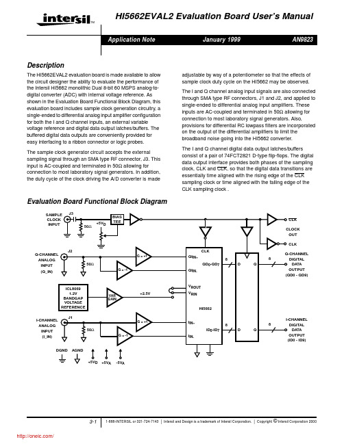
The HI5662 monolithic A/D converter has been designed with separate analog and digital supply and ground pins to keep digital noise out of the analog signal path. The evaluation board provides separate low impedance analog and digital ground planes on layer 2. Since the analog and digital ground planes are connected together at a single point where the power supplies enter the board, DO NOT tie them together back at the power supplies.
/
3-1
1-888-INTERSIL or 321-724-7143 | Intersil and Design is a trademark of Intersil Corporation. | Copyright © Intersil Corporation 2000
集特海光系列
■ 产品特点• 采用2U 19英寸标准机架式机箱• 双路国产申威3231处理器,高速DLI 总线互联, 双向峰值带宽为168.75GB/s 。
• 标准化BMC 模块:支持无缝更换升级模块; • 支持启动介质调整、SOL 、KVM 等功能; • 支持带外升级CPU 固件基于海光平台的单路服务器准系统,该系统 4U 高度,支持 1 颗海光 7100/7200系列 CPU ,最多支持 16 根内存。
本系统使用通用主板,主板名称 G2SERO-B ,可支持 24/36 个 SATA/SAS 硬盘,其中 24 盘位简称 4U24,36 盘位简称 4U36。
■ 应用场景网络安全金融服务运营商能源电力数据处理24盘位36盘位■ 机箱参数项目ASH401-S24REASH401-S36RECPU支持 DDR4 RDIMM/LRDIMM 服务器内存;内存频率支持2133/2400/2666MHz ;支持 8 个DDR4 通道,每个通道支持 2 个 DIMM ,总共支持 16 个DDR4 插槽;支持单条容量为 16GB ,32GB ,64GB ,128GB 整机最大支持2TB 内存容量。
注:为了使系统更稳定,建议使用兼容性列表内存前置支持 24/36 块 3.5 或2.5 英寸热插拔硬盘 后置支持 2 块 2.5 英寸热插拔硬盘 网络功能 支持2个RJ45千兆网口 管理接口 1 个 RJ45 IPMI 管理网口显示功能 Aspeed® AST2500 64MB,由自定义高密度连接器扩展 1 个标准 VGA 接口 M.2 支持 1 个 M.2 接口 外部端口 前置端口:2 个 USB3.0后置端口:1 个 VGA 、2 个 USB3.0、1 个管理网口、2 个 RJ45 数据网口、1个 COM 口 扩展插槽最多支持 10 个 PCIE 扩展插槽(6 个 PCIe 3.0 x8;4 个 PCIe 3.0 x16)电源支持AC 220V 550W 、800W 、1300W 、1600W 冗余电源(根据实际功率适配)支持高压直流240V ~336V 550W 、800W 、1300W 冗余电源 支持低压直流-48V 550W 、800W 、1300W 冗余电源系统风扇 系统支持4个8038温控风扇(选配8056温控风扇) 尺寸695mm*433.4mm*176.5mm (长*宽*高)■ 订购信息名称料号描述GDC-2000 806-001-250101 申威3231处理器*2/32核/2.4G/128GECCDDR4/512GSSD GDC-2000 806-001-250102 申威3231处理器*2/32核/2.4G/256GECCDDR4/512GSSD GDC-2000806-001-250103申威3231处理器*2/32核/2.4G/512GECCDDR4/512GSSD集 特 国 产 系 列集 特 国 产 系 列■ 产品特点• 单个SP3 Socket ,支持海光7100/7200系列处理器 • 总共支持 16 个 DDR4 插槽;整机最大支持 2TB • 单板上面有10组 PCIE 3.0扩展插槽• 1 个 M.2 Key M SSD 插槽,只支持2280 尺寸及PCIe3.0X4信号• 集成了2个千兆网口 ,采用 I350-AM2芯片GME-5001是一款单路 CPU 标准 E-ATX 服务器主板,支持海光 7100、7200 系列处理器。
XCR3256XL_03中文资料

• Optimized for 3.3V systems - Ultra low power operation - 5V tolerant I/O pins with 3.3V core supply - Advanced 0.35 micron five layer metal EEPROM process - Fast Zero Power™ (FZP) CMOS design technology - 3.3V PCI electrical specification compatible outputs (no internal clamp diode on any input or I/O)
Symbol
Parameter
Test Conditions
Min.
Max. Unit
VOH(2) Output High voltage
VCC = 3.0V to 3.6V, IOH = –8 mA
2.4
-
VCC = 2.7V to 3.0V, IOH = –8 mA
LM2576中文资料

LM2576中文资料编辑:D z3w.C o m文章来源:网络我们无意侵犯您的权益,如有侵犯请[联系我们]L M2576中文资料L M2576外形图片L M2576/L M2576H V的特性:1)有3.3V、5V、12V、15V和可调电压输出多种系列;中2)输出电压可调范围1.23V-37V (H V型号的可达57V),负载电压的输出容差最大为±4%;3)最少只需要4个外围组件,可达3A的输出大电流应用电路4)较寛的输入电压范围,H V型号甚至可达40V~60V;5)内部振荡器产生52K H z固定频率;6)可用T T L电平关闭输出,低功耗待机模式,典型待机电流为50μA;7)B U C K式降压器,较高的转换效率;8)过热和过流保护;9)可实现B u c k-B o o s t式正-负电压转换器。
L M2576/L M2576H V引脚功能说明:1)V I N—输入电压端,为减小输入瞬间电压和给调节器提供开关电流,此接脚应接旁路电容C I N;2)O U T P U T—稳压输出端,输出高电压为(V I N-V S AT),输出低电压为-0.5V。
3)G N D—电路地;4)F E E D B A C K—反馈端;电子5)O N/O F F—控制端,高电平有效,待机静态电流仅为75μA图1L M2576内部方框电路图L M2576/L M2576H V外围组件的选择:1)输入电容C I N:要选择低E S R的铝或钽电容作为旁路电容,防止在输入端出现大的瞬间电压。
还有,当你的输入电压波动较大,输出电流有较高,容量一定要选用大些,470μF--10000μF都是可行的选择;电容的电流均方根值至少要为直流负载电流的1/2;基于安全考虑,电容的额定耐压值要为最大输入电压的1.5倍。
千万不要选用陶瓷电容,会造成严重的噪音干扰!N i c h i c o n的铝电解电容不错。
2)肖特基二极管:首选肖特基二极管,因为此类二极管开关速度快、正向压降低、反向恢复时间短,千万不要选用1N4000/1N5400之类的普通整流二极管!3)储能电感:可以看d a t a s h e e t中的电感选择曲线,要求有高的通流量和对应的电感值,也就是说,电感的直流通流量直接影响输出电流。
LPD3256

LPD3256数据手册内建PWM 功能、256 阶灰度调节的LED 智能型灯光驱动芯片LPD3256 芯片是专门为LED 驱动应用设计的芯片,可以应用与LED 显示系统,特别是多离。
散点的级连应用。
LPD3256 提供3 个恒定电流驱动输出,驱动最大电流可达50mA。
LPD3256 芯片内部包括串行移位寄存器和输出寄存器,经串行移位寄存器,串行输入转换为3bit 的并行输出,并把该输出作为输出寄存器的输入,实现芯片级连。
串行移位寄存器和输出寄存器由不同的时钟信号控制,并且都是在诗中信号的上升沿有效。
LPD3256 将控制信号驱动后输出,该输出颗作为后一级电路的输入信号。
LPD3256 工作电压为5V,芯片采用DIP14 或者SOP14 封装。
特点• RGB 三路驱动输出.• 支持恒流/恒压双模式.• 内置1.2MHz 振荡器,支持256 级PWM 输出.• 双线传输结构,需要MCU 少量接口.• 简化外围配套,控制简单,可扩充性好.• 信号输出有放大和整形功能,级联能力强.• IC 脚位抗击静电能力强,即使简易型工厂生产也不容易被损坏.• 通道间和芯片间温度特性和一致性好,亮度偏差小.• 采用独特的IN-RUSH 电流反馈结构,兼容恒压/恒流双模式.• 负载电流直接流过采样电阻.• 直接反馈,采样精度高,一致性好.• 反馈端接地,可以转为恒压驱动模式输出.• CMOS 工艺,最高LED 灯电压可达6V 以上,每路电流可达50mA.• 简化外围配套、降低使用成本.扩充性功能强大.• 驱动一个LED 时可以设置成恒流,也可以设置成恒压驱动.• 在灯电压>6V 时,可设置成外挂三极管驱动模式恒流恒压模式.• 在>6V 高电压供电环境下,可使用简单的稳压管或电阻分压把供电电压降到合适范围内即可工作.• MCU 接口简单,控制便利• 只需占用MCU 的SPI 口或两根GPIO 口线,传输数据量仅为常规方案的1/5-1/3 ,可以使用较低的传输速率.• MCU 将灰度数据移出后,芯片自动按设定的占空比连续输出(FREE-RUN 模式),可以减少甚至不用MCU 缓冲.• 在新数据更新之前,不再需要不停重复刷新数据,可以腾出MCU 时间处理其他事物.• 可使用低成本MCU完成本来可能需要高成本的MCU+CPLD/FPGA架构才能做到的效果• 独特传输协议,可实现较长的级联能力• 输入控制信号频率范围可以从100KHz 到25MHz 的宽范围.• 采用DATA 和DCLK 两根信号线,减低线材连接成本.• 输出端极性反转功能,可以用做「PWM 信号产生器」,可以实现大功率LED 之256 256 级灰度控制• 每级输出时时序上DATA 自动与DCLKO 逐级对齐,不会随级数累积引起偏移误动作.• 内置的时钟再生机制,使DCLK 不会随级联增多改变占空比.• 级联信号采用推挽式强驱动电路,级联间距可达8 米@2MHZ芯片功能框图图1 LPD3256 芯片功能框图芯片封装和管脚说明图2 DIP14 封装图3 SOP14 封装芯片功能时序图图4 LPD3256 时序图交流特性测试电路图5 LPD3256 交流特性测试电路交流特性(VCC=5V, TA=25℃)(VCC=3.3V, TA=25℃)应用系统●LED 装饰照明系统●室内外信息视频显示系统●PWM 信号生成器●LCD TV LED RGB 背光控制器级连应用电路图6 LPD3256 级连应用电路特性曲线图7 输出电流-电源关系曲线图8 反馈电压-温度关系曲线图9 输出电流-输出电压关系曲线图10 输出电流-温度关系曲线图11 CKI-CKO 延时关系曲线(上升沿VCC=3.3V)图12 CKI-CKO 延时关系曲线(下降沿VCC=3.3V)图13 CKI-CKO 延时关系曲线(上升沿VCC=5V)图14 CKI-CKO 延时关系曲线(下降沿VCC=5V)封装。
{售后服务}某某某最新浪潮服务器产品介绍

{售后服务}某某某最新浪潮服务器产品介绍目录1.浪潮NP3020M2服务器22.浪潮NP5020M3服务器53.浪潮NP5540M3服务器84.浪潮NP5580M3服务器125.浪潮NF5140M3服务器166.浪潮NF5240M3服务器217.浪潮NF5270M3服务器248浪潮NF5280M3服务器279.浪潮NF8560M2服务器3010.浪潮NF8520服务器3311.浪潮TS850服务器3612.浪潮NX5760M3刀片服务器3813.浪潮NX5440M3刀片服务器4214.浪潮天梭TS15.浪潮天梭TS16.浪潮天梭TS17.浪潮安全服务器NF5285P25118.浪潮英信SA52245419.浪潮英信SA52455620.浪潮英信SA52435821.浪潮英信SA5212L6122.浪潮英信SA5212S6323.浪潮天梭TS8650G36624.浪潮云海Smartcloud集装箱数据中心6725.浪潮睿捷服务器套件6926.浪潮海量存储系统软件-业务连续保护模块(BCP)71服务器产品介绍1.浪潮NP3020M2服务器产品概述浪潮英信NP3020M2是一款专为中小型应用设计的单路入门级服务器产品,采用全新的平台架构,相比与浪潮上一代产品性能提升40%,可从容的应对各种新业务带来的压力,同时还具有出色的扩展性,能够伴随着业务的增长而增长。
针对中小型应用的特点,NP3020M2具有出色的静音和低辐射设计,更适合办公室环境使用,是中小型信息化建设中入门级服务器的首选。
产品特点1、支持英特尔最新XeonE3-1200系列处理器,大幅提升后的处理器主频,带来更少的延迟和更高计算性能;2、采用支持纠错代码(ECC)的内存,提供比台式机更高水平的数据完整性、可靠性和系统正常运行时间,有效提供数据容错功能,降低系统宕机概率,从容面对不断上涨的业务;3、良好的散热设计,更好的保证机箱内部气流的通畅,确保关键部件正常工作,避免因局部散热不利造成的系统宕机隐患;4、360°静音设计,通过风扇及机箱的优化设计削弱噪音源,智能调控散热能力,从而大幅降低系统噪音,人性化设计全面贯穿健康理念;5、多达6个PCI扩展槽,支持传统PCI及高速PCI-E2.0X16,保护用户现有的IT 设备投资,使用户短期的投资获得长期的超值回报;6、拥有8块硬盘的扩展空间,可选SATA、SAS存储配置,为客户提供更强大的数据存储选择,并提供充足的未来扩展空间产品规格型号NP3020M2处理器英特尔®至强®处理器E3-1200系列,英特尔®奔腾®处理器G850\G860\G620,英特尔®酷睿®处理器I3-2100系列高速缓存3M/8M,随处理器型号不同而不同芯片组英特尔®C202芯片组内存4个内存插槽,支持DDR3ECCunbuffered1066/1333MHz,支持双通道读取硬盘控制器集成6口SATA控制器RAID支持Intelhostraid0,1,10,5(仅windows系统,不支持windows2000及之前版本)硬盘数量标配支持2块SATA硬盘,通过扩展配件最大可支持到8块SATA硬盘I/O扩展槽2个PCI32bit/33MHz;1个PCI-Ex8;2个PCI-Ex1;1个PCI-Ex16集成I/O端口前置:2个USB接口后置:1个标准VGA接口,2个PS/2接口,1个串口,2个RJ45网络接口内置:1个串口,1个USB接口网络控制器支持高性能双千兆网卡,支持网络唤醒、网络冗余、负载均衡等网络高级特性电源300W单电显卡主板集成显示控制器光驱标准DVD光驱软驱可选USB接口的虚拟软驱管理功能支持浪潮睿捷V5.0服务器管理、部署软件支持操作系统MicrosoftServer2003(SP1/SP2)(X32/X64) MicrosoftServer2008(X32、X64) WindowsXPProfessional32bit/64bitWindowsVista32bit/64bit不同配置下操作系统支持能力不同,详情请咨询浪潮公司工作环境温度5℃~35℃电源电压180V~264V(单电)50HZ,90V~264V(双电)50HZ国际认证ISO9001国际质量管理体系ISO14001国际环境管理体系机箱200mm(W)x435mm(H)x510mm(D)参考重量25kg2.浪潮NP5020M3服务器产品概述浪潮英信NP5020M3是浪潮专为中小型企业、政府、教育等客户量身打造的一款双路塔式服务器,完美的静音设计紧凑小巧的内部结构和外观非常特别适合需要小型机箱的零售店或小型办公室环境,采用最新的平台架构及处理器,相对于浪潮上一代产品整体性能提升40%,特别适合像电子政务、电子邮件、文件、打印、OA、ERP、CRM、多媒体教学、中小型数据库、中小型工作站、大型网络的子网系统等。
IMP3256

- Ballast control and half-bridge driver in one IC - Programmable preheat frequency - Programmable preheat time - Internal ignition ramp- Programmable over-current threshold - Programmable run frequency - Programmable dead time - DC bus under-voltage reset - Shutdown pin with hysteresis- Internal 15.6V zener clamp diode on Vcc - Micropower startup (150µA) - Latch immunity and ESD protection - Also available LEAD-FREE (PbF)The 3256 incorporates a high voltage half-bridge gate driver with a programmable oscillator and state diagram to form a complete ballast control IC. The 3256 features include programmable preheat and run frequencies, programmable preheat time, pro-grammable dead-time, and programmable over-current protection. Comprehensive protection features such as protection from failure of a lamp to strike,filament failures, as well as an automatic restart function, have been included in the design. The 3256 is available in both 14 lead PDIP and 14 lead SOIC packages.Key FeaturesGeneral DescriptionTypical ApplicationR BUS R SUPPLYD CP2M1M2C VCC2C VCC1R TR PHC T C VDCC CPHD BOOT NCVCC VDCRTRPH CT CPHVB HO VS C BLO CS SDCOM C CSR CSC SNUBR1L RESC CPD CP1C ELCAP1D RECT2C ELCAP1D RECT1C FILTERF1L FILTERC RES3256PackagesAbsolute Maximum Ratings14 Lead PDIP 14 Lead SOIC (narrow body)Absolute maximum ratings indicate sustained limits beyond which damage to the device may occur. All voltage pa-rameters are absolute voltages referenced to COM, all currents are defined positive into any lead. The thermal resis-tance and power dissipation ratings are measured under board mounted and still air conditions.SymbolDefinitionM i n .Ma x . UnitsV B High side floating supply voltage-0.3 625V V S High side floating supply offset voltage V B - 25 V B + 0.3 V HO High side floating output voltage V S - 0.3 V B + 0.3 V LO Low side output voltage-0.3 V CC + 0.3 I OMAX Maximum allowable output current (HO, LO) due to external power transistor miller effect -500 500 mA V VDC VDC pin voltage -0.3 V CC + 0.3 V V CT CT pin voltage -0.3 V CC + 0.3 I CPH CPH pin current -5 5 mA I RPH RPH pin current -5 5 V RPH RPH pin voltage -0.3 V CC + 0.3 V I RT RT pin current -5 5 mA V RT RT pin voltage-0.3 V CC + 0.3 V V CS Current sense pin voltage -0.3 5.5 I CS Current sense pin current -5 5 mA I SD Shutdown pin current -5 5 I CC Supply current (note 1)-20 20 dV/dt Allowable offset voltage slew rate-50 50 V/ns P D Package power dissipation @ T A ≤ +25°C PD = (T JMAX -T A )/Rth JA(14 pin PDIP)— 1.70 W (14 pin SOIC) — 1.00 Rth JA Thermal resistance, junction to ambient(14 pin PDIP)— 70 /W (14 pin SOIC)— 120 T J Junction temperature -55 150 ℃ T S Storage temperature-55 150 T LLead temperature (soldering, 10 seconds)—300Note 1: This IC contains a zener clamp structure between the chip V CC and COM which has a nominal breakdown voltage of 15.6V. Please note that this supply pin should not be driven by a DC, low impedance power source greater than the VCLAMP specified in the Electrical Characteristics section.Recommended Operating ConditionsBlock DiagramV CCS1S2 40K CT RDT S3RPH CPHVDCSDCompDriverVBHO VSLORR RRRV TH Schmitt1Soft StartFault LogicHigh- Side DriverLow- Side DriverCS 1.3VUnder- Voltage DetectComp5.1V5.1V 10K5.1VFor proper operation the device should be used within the recommended conditions. Symbol Definition M i n . Ma x . Units V Bs High side floating supply voltage V CC - 0.7 V CLAMPV V BSMIN Minimum required V BS voltage for proper HO functionality 5 VCC V S Steady state high side floating supply offset voltage -1 600 V CC Supply voltage V CCUV+ V CLAMP I CC Supply current note 2 10 mA C T CT lead capacitance 220 — pF I SD Shutdown lead current -1 1 mA I CS Current sense lead current -1 1 T J Junction temperature -40 125℃ I SDLK SD pin leakage current (@V SD =6V)— 125 µAI CSLKCS pin leakage current (@V CS =3V)— 25 Note 2: Enough current should be supplied into the V CC lead to keep the internal 15.6V zener clamp diode on this lead regulating its voltage, V CLAMP .Electrical CharacteristicV CC = V BS = V BIAS = 14V +/- 0.25V, V VDC = Open, R T = 39.0kΩ, R PH = 100.0kΩ, C T = 470 pF, V CPH = 0.0V, V CS =0.0V, V SD = 0.0V, C LO, HO = 1000pF, T A = 25oC unless otherwise specified.Symbol Definition Min.T yp.Max.Units T est Conditions Supply CharacteristicsV CCUV+V CC supply undervoltage positive going threshold10.511.512.5V V CC rising from0VV CCUV-V CC supply undervoltage negative going threshold8.59.510.5V CC falling from14V V UVHYS V CC supply undervoltage lockout hysteresis 1.5 2.0 3.0I QCCUV UVLO mode quiescent current50120200µA V CC=11VI QCCFL T Fault-mode quiescent current—200470SD=5.1V,or CS>1.3VI QCC Quiescent V CC supply current— 1.8 2.2mA CT connected toCOM VCC=14V,RT=15k WI QCC50K V CC supply current,f=50kHz— 1.0 1.5RT=33kΩCT=470pF VPCH=14VV CLAMP V CC zener clamp voltage14.515.616.5V I CC=5mA Floating Supply CharacteristicsI QBS0Quiescent V BS supply current-505µA V HO=V S(CT=0V)I QBS1Quiescent V BS supply current—3050 V HO=V B(CT=14V) I LK Offset supply leakage current——50µA V B=V S=600VElectrical Characteristic (Continued)V CC = V BS = V BIAS = 14V +/- 0.25V, V VDC = Open, R T = 39.0kΩ, R PH = 100.0kΩ, C T = 470 pF, V CPH = 0.0V, V CS = 0.0V, V SD = 0.0V, C LO, HO = 1000pF, T A = 25℃unless otherwise specified.Symbol Definition M i n.T y p.Max.Units T est ConditionsOscillator,Ballast Control, I/O Characteristicsfosc Oscillator frequency455055kHz R T=33K, V VDC=5VV CPH=Open (Guaranteed by design)fosc Oscillator frequency90100110KHz R T=15k,R PH=100KC T=470pFd Oscillator duty cycle—45—%V CT+Upper CT ramp voltage threshold—8.3—V Vcc=14V V CT-Lower CT ramp voltage threshold— 4.8—V CTFL T Fault-mode CT pin voltage—0—mV SD>5.1V or CS>1.3V only CT CAP should beconnected to CTt DLO LO output deadtime— 1.5—usect DHO HO output deadtime— 1.5—usecRDT Internal deadtime resistor—3—KΩPreheat CharacteristicsI CPH CPH pin charging current 3.6 4.3 5.2u A V CPH=10V,CT=10V,VDC=5VV CPHFL T Fault-mode CPH pin voltage—0—mV SD>5.1V or CS>1.3V RPH CharacteristicsI RPHLK Open circuit RPH pin leakage current—0.1—u A CT=10VV RPHFL T Fault-mode RPH pin voltage —0—mV SD>5.1V or CS>1.3VRT CharacteristicsI R TLK Open circuit RT pin leakage current—0.1—uA CT=10VV R TFL T Fault-mode RT pin voltage —0—mV SD>5.1V or CS>1.3VProtection CharacteristicsV SDTH+Rising shutdown pin threshold voltage— 5.1—VV SDHYS Shutdown pin threshold hysteresis—450—mVV CSTH Over-current sense threshold voltage 1.1 1.25 1.44Vt CS Over-current sense propogation delay—160—nsec Delay from CS to LOV CSPW Over-current sense minimum pulse width—135—nsec V CS pulse amplitude =VCSTH+100mVR VDC DC bus sensing resistor7.51014KΩV CPH>12V,V CT=0VV DC=7VV CPHVDC CPH to VDC offset voltage10.310.911.4V V CPH=open,V VDC=0V Gate Driver Output CharacteristicsV OL Low-level output voltage—0105mV Io=0V OH High-level output voltage—0100V BIAS-V o,Io=0 tr Turn-on rise time—110150ns C LO=C HO=1nF tf Turn-off fall time—55100State DiagramPower Turned OnUVLO Mode 1/2-Bridge Off I QCC ؆ 120µA CPH = 0VCT = 0V (Oscillator Off)VCC > 11.5V (UV+) andSD < 5.1VVCC < 9.5V(VCC Fault or Power Down) orSD > 5.1V(Lamp Fault or Lamp Removal)PREHEAT Mode1/2-Bridge oscillating @ fPH RPH // RTCPH Charging @ ICPH = 5 µA CS Enabled @ CPH > 7.5V RVDC to COM = 12.6k Ω @ CPH > 7.5VCPH > 10V(End of PREHEAT Mode)Ignition Ramp ModeRPH Open f PH ramps to f RUN CPH chargingRUN Mode RPH = Open1/2-Bridge Oscillating @ fRUNCS > 1.3V (Lamp Fault)CS > 1.3V(Failure to Strike Lamp)FAULT Mode Fault Latch Set 1/2-Bridge Off IQCC ؆ 180µA CPH = 0V VCC = 15.6VCT = 0V (Oscillator Off)CS > 1.3V(Lamp Removal) orSD > 5.1V orVCC < 9.5V (UV-) (Power Turned Off)Typical Performance Characteristics Timing DiagramsNormal operationTypical Performance Characteristics Timing DiagramsNormal operationTypical Performance Characteristics(Continued)DT (µS)C T (p F )Graph 1. CT vs Dead Time (3256)Frequency (KHz)I C C (m A )Graph 2. ICC vs Frequency (3256)V CPH (V)F r e q u e n c y (K H z )Graph 3. Frequency vs V CPH(3256)VDC(V)F r e q u e n c y (K H z )Graph 4. Frequency vs VDC (3256)Typical Performance Characteristics(Continued)V CPH (V)I C P H (p F )Graph 5. I CPH vs V CPH(3256)RT(K Ω)F r e q u e n c y (K H z )Graph 6. Frequency vs RT (3256)V CC (V)I Q C C (m A )Graph 7. IQCC vs V CC (3256)UVLO HysteresisV SS (V)I Q B S (µA )Graph 8. I QBS vs V CC vs Temp(3256)Typical Performance Characteristics(Continued)C S +(V )Temperature °CGraph 9. V CSTH+vs Temperature (3256)Temperature °CR D T (K Ω)Graph 10. RDT vs Temperature (3256)Temperature °CR V D C (K Ω)Graph 11. R VDC+ vs Temperature (3256)Temperature °CU V +,U V -(V )Graph 12. UV+, UV- vs Temperature (3256)Typical Performance Characteristics(Continued)S D +,S D -(V )Temperature °CGraph 13. SD+, SD- vs Temperature (3256)Temperature °CI L K ( µA )Graph 14. ILK vs Temperature (3256)V CC (V)I Q C C ( m A )Graph 15. IQCC vs VCC vs Temperature (3256)V CC (V)I Q C C ( m A )Graph 16. I QCC vs V CC vs Temperature (3256) Internal Zener Diode CurveTypical Performance Characteristics(Continued)V CC (V)I Q C C ( m A )Graph 17. I QCC vs V CC vs Temperature (3256) V CCUV+V CC (V)I Q C C ( µA )Graph 18. I QCC vs V CC vs Temperature (3256) V CCUV+V CC (V)F r e q u e n c y (k H z )Graph 19 F OSC vs V CC vs Temperature (3256) V CPH= 0VF r e q u e n c y (k H z )Temp°(C)Graph 20. FOSC vs Temperature (3256)V CPH = 0VTypical Performance Characteristics(Continued)I C P H ( µA )V CC (V)V CC (V)I C P H ( µA )Graph 21. I CPH vs V CC vs Temperature (3256) V CPH = V CCGraph 22. I CPH vs V CC vs Temperature (3256) V CPH= 0VV CC (V)t D E A D (L O ) ( µS e c )V CC (V)t R I S E (H O ) (n S e c )Graph 23. t DEAD vs V CC vs Temperature (3256) C T = 1nFGraph 24. t RISE(HO) vs V CC vs Temperature (3256)Typical Performance Characteristics(Continued)V CC (V)t F A L L (H O )(n S e c )V CC (V)t R I S E (L O )(n S e c )Graph 25. t FALL(HO) vs V CC vs Temperature (3256)Graph 26. t RISE(LO) vs V CCvs Temperature (3256)V CC (V)t F A L L (H O )(n S e c )Graph 27. t FALL(LO) vs V CC vs Temperature (3256)Functional DescriptionUnder-voltage Lock-Out Mode (UVLO)The under-voltage lock-out mode (UVLO) is defined as the state the IC is in when VCC is below the turn-on threshold of the IC. To identify the different modes of the IC, refer to the State Diagram shown on page 6 of this document. The 3256 undervoltage lock-out is designed to maintain an ultra low supply current of less than 200uA, and to guarantee the IC is fully functional before the high and low side output drivers are activated. Figure 1 shows an efficient supply voltage using the start-up current of the 3256 together with a charge pump from the ballast output stage (RSUPPLY, CVCC, DCP1 and DCP2).3256Figure 1, Start-up and supply circuitry.The start-up capacitor (CVCC) is charged by current through supply resistor (RSUPPLY) minus the start-up current drawn by the IC. This resistor is chosen to provide 2X the maximum start-up current to guarantee ballast start-up at low line input voltage. Once the capacitor voltage on VCC reaches the start-up threshold, and the SD pin is below 4.5 volts, the IC turns on and HO and LO begin to oscillate. The capacitor begins to discharge due to the increase in IC operating current (Figure 2).Functional Description (Continued)Figure 2, Supply capacitor (CVCC) voltage.During the discharge cycle, the rectified current from the charge pump charges the capacitor above the IC turn-off threshold. The charge pump and the internal 15.6V zener clamp of the IC take over as the supply voltage. The start-up capacitor and snubber capacitor must be selected such that enough supply current is available over all ballastoperating conditions. A bootstrap diode (DBOOT) and supply capacitor (CBOOT) comprise the supply voltage for the high side driver circuitry. To guarantee that the high-side supply is charged up before the first pulse on pin HO, the first pulse from the output drivers comes from the LO pin. During undervoltage lock-out mode, the high- and low-side driver outputs HO and LO are both low, pin CT is connected internally to COM to disable the oscillator, and pin CPH is con-nected internally to COM for resetting the preheat time.Preheat Mode (PH)The preheat mode is defined as the state the IC is in when the lamp filaments are being heated to their correct emission temperature. This is necessary for maximizing lamp life and reducing the required ignition voltage. The 3256 enters preheat mode when VCC exceeds the UVLO positive-going threshold. HO and LO begin to oscillate at the preheat frequency with 50% duty cycle and with a dead-time which is set by the value of the external timing capacitor, CT, and internal deadtime resistor, RDT. Pin CPH is disconnected from COM and an internal 4µA current source (Figure 3)Functional Description (Continued)3256Figure 3, Preheat circuitry.charges the external preheat timing capacitor on CPH linearly. The over-current protection on pin CS is disabled during preheat. The preheat frequency is determined by the parallel combination of resistors RT and RPH, together with timing capacitor CT. CT charges and discharges between 1/3 and 3/5 of VCC (see Timing Diagram, page 7). CT is charged exponentially through the parallel combination of RT and RPH connected internally to VCC through MOSFET S1. The charge time of CT from 1/3 to 3/5 VCC is the on-time of the respective output gate driver, HO or LO. Once CT exceeds 3/5 VCC, MOSFET S1 is turned off, disconnecting RT and RPH from VCC. CT is then discharged exponentially through an internal resistor, RDT, through MOSFET S3 to COM. The discharge time of CT from 3/5 to 1/3 VCC is the dead-time (both off) of the output gate drivers, HO and LO. The selected value of CT together with RDT therefore program the desired dead-time (see Design Equations, page 19, Equations 1 and 2). Once CT discharges below 1/3 VCC, MOSFET S3 is turned off, disconnecting RDT from COM, and MOSFET S1 is turned on, connecting RT and RPH again to VCC. The frequency remains at the preheat frequency until the voltage on pin CPH exceeds 13V and the IC enters Ignition Mode. During the preheat mode, both the over-current protection and the DC bus under-voltage reset are en-abled when pin CPH exceeds 7.5V.Ignition Mode (IGN)The ignition mode is defined as the state the IC is in when a high voltage is being established across the lamp necessary for igniting the lamp. The 3256 enters ignition mode when the voltage on pin CPH exceeds 13V.Functional Description (Continued)3256Figure 4, Ignition circuitry.Pin CPH is connected internally to the gate of a p-channel MOSFET (S4) (see Figure 4) that connects pin RPH with pin RT. As pin CPHexceeds 13V, the gate-to-source voltage of MOSFET S4 begins to fall below the turn-on threshold of S4. As pin CPH continues to ramp towards VCC, switch S4 turns off slowly. This results in resistor RPH being disconnected smoothly from resistor RT, which causes the operating frequency to ramp smoothly from the preheat frequency, through the ignition frequency, to the final run frequency. The over-current threshold on pin CS will protect the bal-last against a non-strike or open-filament lamp fault con-dition.The voltage on pin CS is defined by the lower half-bridge MOSFET current flowing through the external current sensing resistor RCS. The resistor RCS therefore programs the maximum allowable peak ignition current (and there-fore peak ignition voltage) of the ballast output stage. The peak ignition current must not exceed the maximum al-lowable current ratings of the output stage MOSFETs. Should this voltage exceed the internal threshold of 1.3V, the IC will enter FAULT modeand both gate driver outputs HO and LO will be latched low.Run Mode (RUN)Once the lamp has successfully ignited, the ballast enters run mode. The run mode is defined as the state the IC is in when the lamp arc is established and the lamp is being driven to a given power level. The run mode oscillating frequency is determined by the timing resistor RT and timing capacitor CT (see Design Equations, page 19, Equations 3 and 4). Should hard-switching occur at the half-bridge at any time due to an openfilament or lamp removal, the voltage across the current sensing resistor, RCS, will exceed the internal threshold of 1.3 volts and the IC will enter FAULT mode. Both gate driver outputs, HO and LO, will be latched low.Functional Description (Continued)DC Bus Under-voltage ResetShould the DC bus decrease too low during a brown-out line condition or over-load condition, the resonant output stage to the lamp can shift near or below resonance. This can produce hardswitching at the half-bridge which can damage the half-bridge switches. To protect against this, pin VDC measures the DC bus voltage and pulls down on pin CPH linearly as the voltage on pin VDC decreases 10.9V below VCC. This causesthe p-channel MOSFET S4 (Figure 4) to close as the DC bus decreases and the frequency to shift higher to a safe operating point above resonance. The DC bus level at which the fre-quency shifting occurs is set by the external RBUS resistor andinternal RVDC resistor. By pulling down on pin CPH, the ignition ramp is also reset. Therefore, should the lamp extin-guish due to very low DC bus levels, the lamp will be auto-matically ignited as the DC bus increases again. The internal RVDC resistor is connected between pin VDC and COM when CPH exceeds 7.5V (during preheat mode).Fault Mode (FAULT)Should the voltage at the current sensing pin, CS, exceed 1.3 volts at any time after the preheat mode, the IC enters fault mode and both gate driver outputs, HO and LO, are latched in the 'low' state. CPH is discharged to COM for resetting the preheat time, and CT is discharged to COM for disabling the oscillator. To exit fault mode, VCC must be recycled back below the UVLO negativegoing turn-off threshold, or, the shutdown pin, SD, must be pulled above 5.1 volts. Either of these will force the IC to enter UVLO mode (see State Dia-gram, page 6). Once VCC is above the turnon threshold and SD is below 4.5 volts, the IC will begin oscillating again in the preheat mode. Design EquationsNote: The results from the following design equations can differ slightly from experimental measurements due to IC tolerances, component tolerances, and os-cillator over- and under-shoot due to internal com-parator response time.Step 1: Program Dead-timeThe dead-time between the gate driver outputs HO and LO is programmed with timing capacitor CT and an internal dead-time resistor RDT. The dead-time is the discharge time of capacitor CT from 3/5VCC to1/3VCC and is given as:[Seconds](1)or[Farads] (2)Step 2: Program Run FrequencyThe final run frequency is programmed with timing resistor RT and timing capacitor CT. The charge timeof capacitor CT from 1/3VCC to 3/5VCC determines the on-time of HO and LO gate driver outputs. The run frequency is therefore given as:[Hertz] (3)[Ohms] (4)orStep 3: Program Preheat FrequencyThe preheat frequency is programmed with timing resistors RT and RPH, and timing capacitor CT. The timing resistors are connected in parallel internally for the duration of the preheat time. The preheat frequency is therefore given as:Functional Description(Continued)[Hertz](5)or[Ohms](6)Step 4: Program Preheat TimeThe preheat time is defined by the time it takesfor the capacitor on pin CPH to charge up to 13 volts (assuming Vcc = 15 volts). An internal current source of 4.3µA flows out of pin CPH. The preheat time is therefore given as:[Seconds ](7)or[Farads](8) Step 5: Program Maximum Ignition CurrentThe maximum ignition current is programmed with the external resistor RCS and an internal threshold of 1.25volts. This threshold determines the overcurrent limit of the ballast, which can be exceeded when the frequencyramps down towards resonance during ignition and thelamp does not[Amps Peak](9)or[Ohms](10) Design Example: 42W-QUAD BIAX CFLNote: The results from the following design example can differ slightly from experimental results due to IC toler-ances, component tolerances, and oscillator over- and under-shoot due to internal comparator response time.Step 1: Program Dead-timeThe dead-time is chosen to be 0.8µs. Using Equation (2) gives the following result:Step 2: Program Run FrequencyThe run frequency is chosen to be 43kHz. Using Equation (4) gives the following result:Step 3: Program Preheat FrequencyThe preheat frequency is chosen such that the lamp filaments are adequately heated within the preheat time. A preheat frequency of 70kHz was chosen. Using Equation (6) gives the following result:Functional Description (Continued) Step 4: Program Preheat TimeThe preheat time of 500ms seconds was chosen. Using Equa-tion (8) gives the following result:Step 5: Program Ignition CurrentThe maximum ignition current is given by the maximum ig-nition voltage and is chosen as 2.0Apk. Using Equation (10)gives the following result:ResultsA fully-functional ballast was designed, built and tested using the calculated values. The values were then adjusted slightly in order to fulfill various ballast parameters (Table 1). The ballast was designed using the 'Typical Application Schematic' given on page 1.parameterDescriptionValueFph Preheat frequency68khz Vph Lamp preheat voltage460vpp Tph Preheat time700ms Rw:Rc Filament preheat ratio4:1 Vign Maximum lgnition voltage1500vpp Tign Lgnition ramp time50ms Frun Running frequency47.5khz Vrun Running lamp voltage180vpk pin Running ballast input power42w Table 1, 42W-Quad Biax Ballast Measured Results Waveform 1. Lamp filament voltage during preheatWaveform 2. Lamp voltage during preheat,ignition and run modesWaveform3, Half-bridge and current sensevoltage during run modeFunctional Description (Continued)Waveform 4, Lamp voltage and currentsense pin during a failure-to-strike lampfault condition.Mechanical Dimensions14-Lead PDIP14-Lead SOIC (narrow body)Bill Of Materialsitem qty Manufacturer1 12 13 14 25 26 17 18 29 1 10 1 11 2 12 1 13 1 14 1 15 2 16 1 17 1 18 1 19 2 20 1 21 1 22 1 23 1 241Total 30DesignatorF1 CFILTER LFILTER DRECT1,DRECT2 CE-CAP1,CELCAP2LRES CCP DCP1,DCP2 CRES CSNUM M1,M2 RCS R1 CCS CBOOT,CVCC1CVCC2 DBOOT IC1 RSUPPLY,RBUSRT CT RPH CPH CVDCescrignator Fuse Filter capacitor Filter inductor Rectifier diode Electrolytic capacitor Resonant inductor Charge pump capacitor Charge pump diodes Resonant capacitor Snubber capacitor Half-bridge MOSFET Current sense resistor Limint resistor Filter resistor Supply capacitor Supply capacitor Bootstrap diode Ballast control ICResistor Timing resistor Timing capacitor Preheat resistor Preheat capacitorcapacitorValue 0.1µF/400V 330µH/0.5A 1N4007 47µF /250V 1.25mH /1.5A 470pF/1kV 1N4148 6.8nF/1kV 470pF/1kV IRF730 0.75R/0.5W 1K/0.25W 470pF/16V 0.1µF/25V 2.2µF/25V 10DF6 1M/0.25W 39K/0.25W 470pF/25V 75K/0.25W 0.22µF/25V 0.01µF/25VPart NO.LEADFREE PART MARKING INFORMATIONISO 9001 RegisteredDaily Silver IMP Microelectronics Co.,Ltd 7 keda Road ,Hi-Tech Park, NingBo,Zhejiang,P.R.C Post Code:315040Tel:(086)-574-87906358Fax:(086)-574-87908866Email:sales@ The IMP logo is a registered trademark of Daily Silver IMP. All other company and product names are trademarks of their respective owners@2010 Daily Silver IMP Printed in chinaRevision: CIssue Date: 12th.Mar.2010Type: ProductOrdering InformationMARKING CODE Lead Free Released Non-Lead Free ReleasedAssembly site code Per SCOP 200-002Lot Code(Prod mode - 4 digit SPN code)Part numberDate codeIMPIMP logoBasic Part (Non-Lead Free) 14-Lead PDIP 3256 order 3256 14-Lead SOIC 3256S order 3256SLeadfree Part14-Lead PDIP 3256 order 3256PbF 14-Lead SOIC 3256S order 3256SPbF。
- 1、下载文档前请自行甄别文档内容的完整性,平台不提供额外的编辑、内容补充、找答案等附加服务。
- 2、"仅部分预览"的文档,不可在线预览部分如存在完整性等问题,可反馈申请退款(可完整预览的文档不适用该条件!)。
- 3、如文档侵犯您的权益,请联系客服反馈,我们会尽快为您处理(人工客服工作时间:9:00-18:30)。
Supply Voltage (AVCC , DVCC1, DVCC2) . . . . . . . . . . -0.5V to +7.0V (DGND3) . . . . . . . . . . . . . . . . . . . . . . . . . . . . . . . . -0.5V to +7.0V (DVEE3) . . . . . . . . . . . . . . . . . . . . . . . . . . . . . . . . . -7.0V to +0.5V (DGND3 - DVEE3) . . . . . . . . . . . . . . . . . . . . . . . . . -0.5V to +7.0V Analog Input Voltage (VIN). . . . . . . . . . . . . . . . . VRT - 2.7V to AVCC Reference Input Voltage (VRT). . . . . . . . . . . . . . . . . +2.7V to AVCC (VRB) . . . . . . . . . . . . . . . . . . . . . . . . . . . . . . . .VIN - 2.7V to AVCC (|VRT - VRB|) . . . . . . . . . . . . . . . . . . . . . . . . . . . . . . . . . . . +2.5V Digital Input Voltage PECL/ECL . . . . . . . . . . . . . . . . . . . DVEE3 - 0.5 to DGND3 + 0.5 TTL . . . . . . . . . . . . . . . . . . . . . . . . . DGND3 - 0.5 to DVCC1 + 0.5 VID (|***/E - ***N/E| (Note 2)) . . . . . . . . . . . . . . . . . . . . . . . . . 2.7V
• Magnetic Recording (PRML)
Pinout
RESETN/E RESET/E RESETN/T
HI3256 (LQFP) TOP VIEW
SELECT1 INV CLKOUT DVCC2 DGND2
PBD7
PBD6 PBD5
DVEE3 VRB AGND VRM1 AVCC VIN VRM2 AVCC VRM3 AGND VRAD7
15 13
AGND
SELECT1 DGND1
DGND2
2
元器件交易网
HI3256
Absolute Maximum Ratings
TA = 25oC
Thermal Information
Thermal Resistance (Typical, Note 1) θJA (oC/W) LQFP Package . . . . . . . . . . . . . . . . . . . . . . . . . . . . . 65 Maximum Junction Temperature . . . . . . . . . . . . . . . . . . . . . . 150oC Maximum Storage Temperature Range . . . . . . . . . . -65oC to 150oC Maximum Lead Temperature (Soldering 10s) . . . . . . . . . . . . .300oC (Lead Tips Only)
元器件交易网
HI3256
Data Sheet June 1999 File Number 4642.1
8-Bit, 120MSPS, Flash A/D Converter
The HI3256 is an 8-bit, high-speed, flash analog-to-digital converter optimized for high speed, low power, and ease of use. With a 120MSPS encode rate capability and full-power analog bandwidth of 250MHz, this component is ideal for applications requiring the highest possible dynamic performance. To minimize system cost and power dissipation, only a +5V power supply is required. The HI3256 clock input interfaces directly to TTL, ECL or PECL logic and will operate with singleended inputs. The user may select 16-bit demultiplexed output or 8-bit single channel digital outputs. The demultiplexed mode interleaves the data through two 8-bit channels at 1/2 the clock rate. Operation in demultiplexed mode reduces the speed and cost of external digital interfaces, while allowing the A/D converter to be clocked to the full 120MSPS conversion rate. Fabricated with an advanced Bipolar process, the HI3256 is provided in a space-saving 48-lead LQFP surface mount plastic package and is specified over the -20oC to 75oC temperature range.
PAD3
元器件交易网
HI3256 Block Diagram
AVCC 5 VRT 11 R1 R/2 R/2 1 R 39 PBD6 2 R 63 VRM3 9 R 64 R 35 PBD2 65 6 BITS R 126 R 127 VRM2 VIN 7 6 R 129 6 BITS R 191 VRM1 4 R LATCHB TTLOUT 192 R 193 R 254 R 255 R/2 VRB CLK/T CLK/E CLKN/E 2 R/2 21 PAD0 (LSB) DELAY 16 SELECT2 17 VOCLP 18 PS 14 D RESETN/T RESETN/E RESET/E 46 48 47 3 10 45 29 20 32 41 1 DVEE3 Q SELECT1 Q 43 CLKOUT 6 BITS 23 PAD2 22 PAD1 26 PAD5 25 PAD4 24 PAD3 27 PAD6 R 128 ENCODER 6-BIT LATCH AND ENCODER 34 PBD1 33 P1D0 (LSB) 8 BITS 6 BITS 38 PBD5 LATCHA TTLOUT 37 PBD4 36 PBD3 (MSB) 40 PBD7 8 INV 44 DVCC1 30 DVCC2 19 31 42 DGND3 12
26 11 25 12 13 14 15 16 17 18 19 20 21 22 23 24
CLK/T SELECT2
DVCC2
CLKN/E
DGND2 PAD0 PAD1
VOCLP
CLK/E
PS
PAD2
1
CAUTION: These devices are sensitive to electrostatic discharge; follow proper IC Handling Procedures. 1-888-INTERSIL or 321-724-7143 | Copyright © Intersil Corporation 1999
Applications
• LCD/PDP Monitors and Projectors (RGB Video) • Digital Oscilloscopes • Digital Communications (QPSK, QAM)
Ordering Information
PART NUMBER HI3256JCQ TEMP. RANGE (oC) -20 to 75 PACKAGE 48 Ld LQFP PKG. NO. Q48.7x7-S
1 2 3 4 5 6 7 8 9 10
48 47 46 45 44 43 42 41 40 39 38 37 36 35 34 33 32 31 30 29 28 27
PBD4
PBD3 PBD2 PBD1 PBD0 DGND2 DVCC2 DVCC1 DGND1 PAD7 PAD6 PAD5 PAD4
Features
• Differential Linearity Error. . . . . . . . . . . . . . . . . . ±0.5 LSB • Integral Linearity Error . . . . . . . . . . . . . . . . . . . . ±0.5 LSB • Low Input Capacitance . . . . . . . . . . . . . . . . . . . . . . . 10pF • Wide Analog Input Bandwidth . . . . . . . . . . . . . . . 250MHz • Low Power Consumption . . . . . . . . . . . . . . . . . . . 500mW • Output Voltage Control Function (VOCLP pin) • 1:2 Demultiplexed Output Pin • Internal 1/2 Frequency Divider Circuit (w/Reset Function) • CLK/2 Clock Output • Compatible with PECL, ECL and TTL Digital Input Levels • Direct Replacement for Sony CXA3256R