74AC14
74LCX14中文资料

1/8September 2001s 5V TOLERANT INPUTS sHIGH SPEED :t PD = 5.0ns (MAX.) at V CC = 3VsPOWER DOWN PROTECTION ON INPUTS AND OUTPUTSsSYMMETRICAL OUTPUT IMPEDANCE:|I OH | = I OL = 24mA (MIN) at V CC = 3Vs PCI BUS LEVELS GUARANTEED AT 24 mA sBALANCED PROPAGATION DELAYS:t PLH ≅ t PHLsOPERATING VOLTAGE RANGE:V CC (OPR) = 2.0V to 3.6V (1.5V Data Retention)sPIN AND FUNCTION COMPATIBLE WITH 74 SERIES 14sLATCH-UP PERFORMANCE EXCEEDS 500mA (JESD 17)sESD PERFORMANCE:HBM > 2000V (MIL STD 883 method 3015); MM > 200VDESCRIPTIONThe 74LCX14 is a low voltage CMOS HEX SCHMITT INVERTER fabricated with sub-micron silicon gate and double-layer metal wiring C 2MOS technology. It is ideal for low power and high speed 3.3V applications. It can be interfaced to 5V signal environment for inputsIt has same speed performance at 3.3V than 5V AC/ACT family, combined with a lower power consumption.Pin configuration and function are the same as those of the 74LCX04 but the 74LCX14 has hysteresis between the positive and negative input threshold typically of 0.8V.This together with its schmitt trigger function allows it to be used on line receivers with slow rise/fall input signals.All inputs and outputs are equipped with protection circuits against static discharge, giving them 2KV ESD immunity and transient excess voltage.74LCX14LOW VOLTAGE CMOS HEX SCHMITT INVERTERWITH 5V TOLERANT INPUTSPIN CONNECTION AND IEC LOGIC SYMBOLSORDER CODESPACKAGE TUBE T & R SOP 74LCX14M74LCX14MTR TSSOP74LCX14TTR74LCX142/8INPUT AND OUTPUT EQUIVALENT CIRCUITPIN DESCRIPTIONTRUTH TABLEABSOLUTE MAXIMUM RATINGSAbsolute Maximum Ratings are those values beyond which damage to the device may occur. Functional operation under these conditions is not implied1) I O absolute maximum rating must be observed 2) V O < GNDPIN No SYMBOL NAME AND FUNCTION 1, 3, 5, 9 ,11,131A to 6A Data Inputs 2, 4, 6, 8, 10,121Y to 6Y Data Outputs 7GND Ground (0V)14V CCPositive Supply VoltageA Y L H HLSymbol ParameterValue Unit V CC Supply Voltage -0.5 to +7.0V V I DC Input Voltage-0.5 to +7.0V V O DC Output Voltage (V CC = 0V)-0.5 to +7.0V V O DC Output Voltage (High or Low State) (note 1)-0.5 to V CC + 0.5V I IK DC Input Diode Current- 50mA I OK DC Output Diode Current (note 2)- 50mA I O DC Output Current± 50mA I CC DC Supply Current per Supply Pin ± 100mA I GND DC Ground Current per Supply Pin ± 100mA T stg Storage Temperature -65 to +150°C T LLead Temperature (10 sec)300°C74LCX143/8RECOMMENDED OPERATING CONDITIONS1) Truth Table guaranteed: 1.5V to 3.6VDC SPECIFICATIONSDYNAMIC SWITCHING CHARACTERISTICS1) Number of outputs defined as "n". Measured with "n-1" outputs switching from HIGH to LOW or LOW to HIGH. The remaining output is measured in the LOW state.Symbol ParameterValue Unit V CC Supply Voltage (note 1) 2.0 to 3.6V V I Input Voltage0 to 5.5V V O Output Voltage (V CC = 0V)0 to 5.5V V O Output Voltage (High or Low State)0 to V CC V I OH , I OL High or Low Level Output Current (V CC = 3.0 to 3.6V)± 24mA I OH , I OL High or Low Level Output Current (V CC = 2.7V)± 12mA T opOperating Temperature-55 to 125°CSymbolParameterTest ConditionValueUnitV CC (V)-40 to 85 °C -55 to 125 °C Min.Max.Min.Max.V T+Positive Input threshold3.0 1.2 2.2 1.2 2.2V V T-Negative Input threshold3.00.6 1.50.6 1.5V V H Hysteresis Voltage 3.00.4 1.20.4 1.2V V OHHigh Level Output Voltage2.7 to3.6I O =-100 µA V CC -0.2V CC -0.2V2.7I O =-12 mA 2.2 2.23.0I O =-18 mA 2.4 2.4I O =-24 mA 2.22.2V OLLow Level Output Voltage2.7 to3.6I O =100 µA 0.20.2V 2.7I O =12 mA 0.40.43.0I O =16 mA 0.40.4I O =24 mA 0.550.55I I Input Leakage Current2.7 to3.6V I = 0 to 5.5V ± 5± 5µA I off Power Off Leakage Current0V I or V O = 5.5V 1010µA I CC Quiescent Supply Current2.7 to3.6V I = V CC or GND 1010µA V I or V O = 3.6 to 5.5V ± 10± 10∆I CCI CC incr. per Input2.7 to3.6V IH = V CC - 0.6V500500µA SymbolParameterTest ConditionValue UnitV CC (V)T A = 25 °C Min.Typ.Max.V OLP Dynamic Low Level Quiet Output (note 1)3.3C L = 50pFV IL = 0V, V IH = 3.3V0.8V V OLV-0.874LCX144/8AC ELECTRICAL CHARACTERISTICS1) Skew is defined as the absolute value of the difference between the actual propagation delay for any two outputs of the same device switch-ing in the same direction, either HIGH or LOW (t OSLH = | t PLHm - t PLHn |, t OSHL = | t PHLm - t PHLn |)2) Parameter guaranteed by designCAPACITIVE CHARACTERISTICS1) C PD is defined as the value of the IC’s internal equivalent capacitance which is calculated from the operating current consumption without load. (Refer to Test Circuit). Average operating current can be obtained by the following equation. I CC(opr) = C PD x V CC x f IN + I CC /6 (per gate)TEST CIRCUITL R L = 500Ω or equivalentR T = Z OUT of pulse generator (typically 50Ω)SymbolParameterTest ConditionValueUnitV CC (V)C L (pF)R L (Ω)t s = t r (ns)-40 to 85 °C -55 to 125 °C Min.Max.Min.Max.t PLH t PHL Propagation Delay Time2.750500 2.5 6.5 6.5ns3.0 to 3.6 1.55.0 1.55.0t OSLH t OSHLOutput To Output Skew Time (note1, 2)3.0 to 3.6505002.51.01.0ns SymbolParameterTest ConditionValue UnitV CC (V)T A = 25 °C Min.Typ.Max.C IN Input Capacitance3.3V IN = 0 to V CC 6pF C PDPower Dissipation Capacitance (note 1)3.3f IN = 10MHz V IN = 0 or V CC48pF74LCX145/8WAVEFORM : PROPAGATION DELAY(f=1MHz; 50% duty cycle)74LCX14Information furnished is believed to be accurate and reliable. However, STMicroelectronics assumes no responsibility for the consequences of use of such information nor for any infringement of patents or other rights of third parties which may result from its use. No license is granted by implication or otherwise under any patent or patent rights of STMicroelectronics. Specifications mentioned in this publication are subject to change without notice. This publication supersedes and replaces all information previously supplied. STMicroelectronics products are not authorized for use as critical components in life support devices or systems without express written approval of STMicroelectronics.© The ST logo is a registered trademark of STMicroelectronics© 2000 STMicroelectronics - Printed in Italy - All Rights ReservedSTMicroelectronics GROUP OF COMPANIESAustralia - Brazil - China - Finland - France - Germany - Hong Kong - India - Italy - Japan - Malaysia - Malta - MoroccoSingapore - Spain - Sweden - Switzerland - United Kingdom© 8/8。
74系列芯片功能总汇
74系列芯片功能总汇1.基本逻辑门芯片:-74LS00:四输入与非门-74LS02:四输入与门-74LS04:六反相器门-74LS08:四输入与门-74LS32:四输入或门2.触发器芯片:-74LS74:双D触发器-74LS76:双JK触发器3.移位寄存器芯片:-74LS95:四位并行存储器-74LS164:八位串行输入并行输出移位寄存器4.计数器芯片:-74LS90:十进制计数器-74LS93:二进制计数器-74LS191:四位并行访问计数器5.译码器/编码器芯片:-74LS138:三到八译码器-74LS148:八到三译码器-74LS151:八输入多路选择器6.多路开关芯片:-74LS151:八输入多路选择器-74LS153:双四输入多路选择器-74LS157:四输入数据选择/多功能门7.模拟开关芯片:-74LS240:八位双向缓冲器-74LS541:八位缓冲/驱动器8.显示驱动芯片:-74LS47:BCD-七段LED显示驱动器9.存储器芯片:-74LS85:四位二进制比较器-74LS86:四输入异或门-74LS138:三到八译码器10.时序逻辑芯片:-74LS121:单稳态多谐振荡器-74LS123:可编程多谐振荡器-74LS125:四路三态缓冲器11.数据选择器/复用器芯片:-74LS151:八输入多路选择器-74LS153:双四输入多路选择器12.数据驱动器芯片:-74LS244:八位缓冲/驱动器13.时钟频率分频器芯片:-74LS390:双五位二进制分频器14.辅助功能芯片:-74LS368:八位全通滤波器-74LS393:双四位二进制计数器15.存储器扩展芯片:-74LS670:四位四进制加法器-74LS688:八位比较器/译码器16.控制器芯片:-74LS592:八位可移位输入存储器-74LS595:八位移位存储器这些仅仅是74系列芯片中的一小部分,并且还有许多其他功能的芯片未被列举出来。
SN74AC14DRG4资料

IMPORTANT NOTICETexas Instruments Incorporated and its subsidiaries(TI)reserve the right to make corrections,modifications,enhancements, improvements,and other changes to its products and services at any time and to discontinue any product or service without notice. Customers should obtain the latest relevant information before placing orders and should verify that such information is current and complete.All products are sold subject to TI’s terms and conditions of sale supplied at the time of order acknowledgment.TI warrants performance of its hardware products to the specifications applicable at the time of sale in accordance with TI’s standard warranty.Testing and other quality control techniques are used to the extent TI deems necessary to support this warranty.Except where mandated by government requirements,testing of all parameters of each product is not necessarily performed.TI assumes no liability for applications assistance or customer product design.Customers are responsible for their products and applications using TI components.To minimize the risks associated with customer products and applications,customers should provide adequate design and operating safeguards.TI does not warrant or represent that any license,either express or implied,is granted under any TI patent right,copyright,mask work right,or other TI intellectual property right relating to any combination,machine,or process in which TI products or services are rmation published by TI regarding third-party products or services does not constitute a license from TI to use such products or services or a warranty or endorsement e of such information may require a license from a third party under the patents or other intellectual property of the third party,or a license from TI under the patents or other intellectual property of TI. Reproduction of information in TI data books or data sheets is permissible only if reproduction is without alteration and is accompanied by all associated warranties,conditions,limitations,and notices.Reproduction of this information with alteration is an unfair and deceptive business practice.TI is not responsible or liable for such altered documentation.Resale of TI products or services with statements different from or beyond the parameters stated by TI for that product or service voids all express and any implied warranties for the associated TI product or service and is an unfair and deceptive business practice.TI is not responsible or liable for any such statements.TI products are not authorized for use in safety-critical applications(such as life support)where a failure of the TI product would reasonably be expected to cause severe personal injury or death,unless officers of the parties have executed an agreement specifically governing such use.Buyers represent that they have all necessary expertise in the safety and regulatory ramifications of their applications,and acknowledge and agree that they are solely responsible for all legal,regulatory and safety-related requirements concerning their products and any use of TI products in such safety-critical applications,notwithstanding any applications-related information or support that may be provided by TI.Further,Buyers must fully indemnify TI and its representatives against any damages arising out of the use of TI products in such safety-critical applications.TI products are neither designed nor intended for use in military/aerospace applications or environments unless the TI products are specifically designated by TI as military-grade or"enhanced plastic."Only products designated by TI as military-grade meet military specifications.Buyers acknowledge and agree that any such use of TI products which TI has not designated as military-grade is solely at the Buyer's risk,and that they are solely responsible for compliance with all legal and regulatory requirements in connection with such use.TI products are neither designed nor intended for use in automotive applications or environments unless the specific TI products are designated by TI as compliant with ISO/TS16949requirements.Buyers acknowledge and agree that,if they use anynon-designated products in automotive applications,TI will not be responsible for any failure to meet such requirements. Following are URLs where you can obtain information on other Texas Instruments products and application solutions:Products ApplicationsAmplifiers Audio /audioData Converters Automotive /automotiveDSP Broadband /broadbandInterface Digital Control /digitalcontrolLogic Military /militaryPower Mgmt Optical Networking /opticalnetworkMicrocontrollers Security /securityLow Power /lpw Telephony /telephonyWirelessVideo&Imaging /videoWireless /wirelessMailing Address:Texas Instruments,Post Office Box655303,Dallas,Texas75265Copyright©2007,Texas Instruments IncorporatedPACKAGING INFORMATIONOrderable Device Status(1)PackageType PackageDrawingPins PackageQtyEco Plan(2)Lead/Ball Finish MSL Peak Temp(3)5962-87624012A ACTIVE LCCC FK201TBD POST-PLATE N/A for Pkg Type 5962-8762401CA ACTIVE CDIP J141TBD A42SNPB N/A for Pkg Type 5962-8762401DA ACTIVE CFP W141TBD A42N/A for Pkg Type 5962-8762401VCA ACTIVE CDIP J141TBD A42SNPB N/A for Pkg Type 5962-8762401VDA ACTIVE CFP W141TBD A42N/A for Pkg Type SN74AC14D ACTIVE SOIC D1450Green(RoHS&no Sb/Br)CU NIPDAU Level-1-260C-UNLIMSN74AC14DBLE OBSOLETE SSOP DB14TBD Call TI Call TISN74AC14DBR ACTIVE SSOP DB142000Green(RoHS&no Sb/Br)CU NIPDAU Level-1-260C-UNLIMSN74AC14DBRE4ACTIVE SSOP DB142000Green(RoHS&no Sb/Br)CU NIPDAU Level-1-260C-UNLIMSN74AC14DBRG4ACTIVE SSOP DB142000Green(RoHS&no Sb/Br)CU NIPDAU Level-1-260C-UNLIMSN74AC14DE4ACTIVE SOIC D1450Green(RoHS&no Sb/Br)CU NIPDAU Level-1-260C-UNLIMSN74AC14DG4ACTIVE SOIC D1450Green(RoHS&no Sb/Br)CU NIPDAU Level-1-260C-UNLIMSN74AC14DR ACTIVE SOIC D142500Green(RoHS&no Sb/Br)CU NIPDAU Level-1-260C-UNLIMSN74AC14DRE4ACTIVE SOIC D142500Green(RoHS&no Sb/Br)CU NIPDAU Level-1-260C-UNLIMSN74AC14DRG4ACTIVE SOIC D142500Green(RoHS&no Sb/Br)CU NIPDAU Level-1-260C-UNLIMSN74AC14N ACTIVE PDIP N1425Pb-Free(RoHS)CU NIPDAU N/A for Pkg TypeSN74AC14NE4ACTIVE PDIP N1425Pb-Free(RoHS)CU NIPDAU N/A for Pkg TypeSN74AC14NSR ACTIVE SO NS142000Green(RoHS&no Sb/Br)CU NIPDAU Level-1-260C-UNLIMSN74AC14NSRE4ACTIVE SO NS142000Green(RoHS&no Sb/Br)CU NIPDAU Level-1-260C-UNLIMSN74AC14NSRG4ACTIVE SO NS142000Green(RoHS&no Sb/Br)CU NIPDAU Level-1-260C-UNLIMSN74AC14PW ACTIVE TSSOP PW1490Green(RoHS&no Sb/Br)CU NIPDAU Level-1-260C-UNLIMSN74AC14PWE4ACTIVE TSSOP PW1490Green(RoHS&no Sb/Br)CU NIPDAU Level-1-260C-UNLIMSN74AC14PWG4ACTIVE TSSOP PW1490Green(RoHS&no Sb/Br)CU NIPDAU Level-1-260C-UNLIM SN74AC14PWLE OBSOLETE TSSOP PW14TBD Call TI Call TISN74AC14PWR ACTIVE TSSOP PW142000Green(RoHS&no Sb/Br)CU NIPDAU Level-1-260C-UNLIMSN74AC14PWRE4ACTIVE TSSOP PW142000Green(RoHS&no Sb/Br)CU NIPDAU Level-1-260C-UNLIMSN74AC14PWRG4ACTIVE TSSOP PW142000Green(RoHS&no Sb/Br)CU NIPDAU Level-1-260C-UNLIM SNJ54AC14FK ACTIVE LCCC FK201TBD POST-PLATE N/A for Pkg Type 9-Oct-2007Orderable Device Status (1)Package Type Package DrawingPins Package Qty Eco Plan (2)Lead/Ball Finish MSL Peak Temp (3)SNJ54AC14J ACTIVE CDIP J 141TBD A42SNPB N /A for Pkg Type SNJ54AC14WACTIVECFPW141TBDA42N /A for Pkg Type(1)The marketing status values are defined as follows:ACTIVE:Product device recommended for new designs.LIFEBUY:TI has announced that the device will be discontinued,and a lifetime-buy period is in effect.NRND:Not recommended for new designs.Device is in production to support existing customers,but TI does not recommend using this part in a new design.PREVIEW:Device has been announced but is not in production.Samples may or may not be available.OBSOLETE:TI has discontinued the production of the device.(2)Eco Plan -The planned eco-friendly classification:Pb-Free (RoHS),Pb-Free (RoHS Exempt),or Green (RoHS &no Sb/Br)-please check /productcontent for the latest availability information and additional product content details.TBD:The Pb-Free/Green conversion plan has not been defined.Pb-Free (RoHS):TI's terms "Lead-Free"or "Pb-Free"mean semiconductor products that are compatible with the current RoHS requirements for all 6substances,including the requirement that lead not exceed 0.1%by weight in homogeneous materials.Where designed to be soldered at high temperatures,TI Pb-Free products are suitable for use in specified lead-free processes.Pb-Free (RoHS Exempt):This component has a RoHS exemption for either 1)lead-based flip-chip solder bumps used between the die and package,or 2)lead-based die adhesive used between the die and leadframe.The component is otherwise considered Pb-Free (RoHS compatible)as defined above.Green (RoHS &no Sb/Br):TI defines "Green"to mean Pb-Free (RoHS compatible),and free of Bromine (Br)and Antimony (Sb)based flame retardants (Br or Sb do not exceed 0.1%by weight in homogeneous material)(3)MSL,Peak Temp.--The Moisture Sensitivity Level rating according to the JEDEC industry standard classifications,and peak solder temperature.Important Information and Disclaimer:The information provided on this page represents TI's knowledge and belief as of the date that it is provided.TI bases its knowledge and belief on information provided by third parties,and makes no representation or warranty as to the accuracy of such information.Efforts are underway to better integrate information from third parties.TI has taken and continues to take reasonable steps to provide representative and accurate information but may not have conducteddestructive testing or chemical analysis on incoming materials and chemicals.TI and TI suppliers consider certain information to be proprietary,and thus CAS numbers and other limited information may not be available for release.In no event shall TI's liability arising out of such information exceed the total purchase price of the TI part(s)at issue in this document sold by TI to Customer on an annual basis.9-Oct-2007TAPE AND REEL BOXINFORMATIONDevicePackage Pins SiteReel Diameter (mm)Reel Width (mm)A0(mm)B0(mm)K0(mm)P1(mm)W (mm)Pin1Quadrant SN74AC14DBR DB 14SITE 41330168.2 6.6 2.51216Q1SN74AC14DR D 14SITE 2733016 6.59.0 2.1816Q1SN74AC14DR D 14SITE 4133016 6.59.0 2.1816Q1SN74AC14NSR NS 14SITE 41330168.210.5 2.51216Q1SN74AC14PWRPW14SITE 41330127.05.61.6812Q14-Oct-2007DevicePackage Pins Site Length (mm)Width (mm)Height (mm)SN74AC14DBR DB 14SITE 41346.0346.033.0SN74AC14DR D 14SITE 27342.9336.628.58SN74AC14DR D 14SITE 41346.0346.033.0SN74AC14NSR NS 14SITE 41346.0346.033.0SN74AC14PWRPW14SITE 41346.0346.029.04-Oct-2007。
74AC14 六角施密特触发器
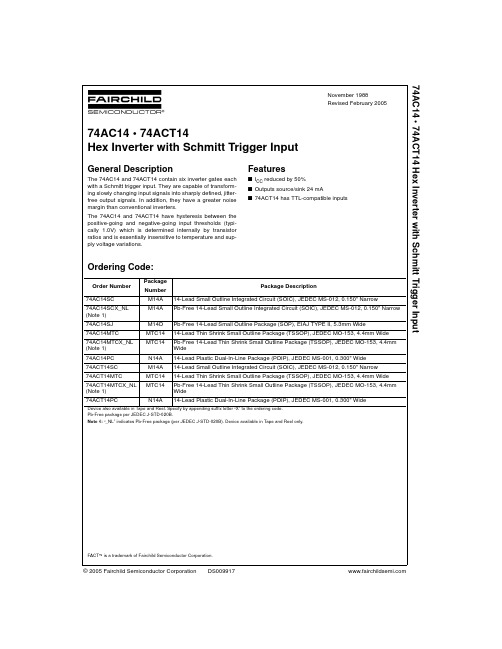
© 2005 Fairchild Semiconductor Corporation DS009917November 1988Revised February 200574AC14 • 74ACT14 Hex Inverter with Schmitt Trigger Input74AC14 • 74ACT14Hex Inverter with Schmitt Trigger InputGeneral DescriptionThe 74AC14 and 74ACT14 contain six inverter gates each with a Schmitt trigger input. They are capable of transform-ing slowly changing input signals into sharply defined, jitter-free output signals. In addition, they have a greater noise margin than conventional inverters.The 74AC14 and 74ACT14 have hysteresis between the positive-going and negative-going input thresholds (typi-cally 1.0V) which is determined internally by transistor ratios and is essentially insensitive to temperature and sup-ply voltage variations.Featuress I CC reduced by 50%s Outputs source/sink 24 mAs 74ACT14 has TTL-compatible inputsOrdering Code:Device also available in Tape and Reel. Specify by appending suffix letter “X” to the ordering code.Pb-Free package per JEDEC J-STD-020B.Note 1: “_NL” indicates Pb-Free package (per JEDEC J-STD-020B). Device available in Tape and Reel only.FACT ¥ is a trademark of Fairchild Semiconductor Corporation.Order Number Package Package DescriptionNumber 74AC14SC M14A 14-Lead Small Outline Integrated Circuit (SOIC), JEDEC MS-012, 0.150" Narrow 74AC14SCX_NL (Note 1)M14A Pb-Free 14-Lead Small Outline Integrated Circuit (SOIC), JEDEC MS-012, 0.150" Narrow 74AC14SJ M14D Pb-Free 14-Lead Small Outline Package (SOP), EIAJ TYPE II, 5.3mm Wide74AC14MTC MTC1414-Lead Thin Shrink Small Outline Package (TSSOP), JEDEC MO-153, 4.4mm Wide 74AC14MTCX_NL (Note 1)MTC14Pb-Free 14-Lead Thin Shrink Small Outline Package (TSSOP), JEDEC MO-153, 4.4mm Wide74AC14PC N14A 14-Lead Plastic Dual-In-Line Package (PDIP), JEDEC MS-001, 0.300" Wide 74ACT14SC M14A 14-Lead Small Outline Integrated Circuit (SOIC), JEDEC MS-012, 0.150" Narrow 74ACT14MTC MTC1414-Lead Thin Shrink Small Outline Package (TSSOP), JEDEC MO-153, 4.4mm Wide 74ACT14MTCX_NL (Note 1)MTC14Pb-Free 14-Lead Thin Shrink Small Outline Package (TSSOP), JEDEC MO-153, 4.4mm Wide74ACT14PCN14A14-Lead Plastic Dual-In-Line Package (PDIP), JEDEC MS-001, 0.300" Wide 274A C 14 • 74A C T 14Logic SymbolIEEE/IECPin DescriptionsConnection DiagramFunction TablePin Names Description I n Inputs O nOutputsInput Output A O L H HL74AC14 • 74ACT14Absolute Maximum Ratings (Note 2)Recommended Operating ConditionsNote 2: Absolute maximum ratings are those values beyond which damage to the device may occur. The databook specifications should be met, with-out exception, to ensure that the system design is reliable over its power supply, temperature, and output/input loading variables. Fairchild does not recommend operation of FACT ¥ circuits outside databook specifications.DC Electrical Characteristics for ACNote 3: All outputs loaded; thresholds on input associated with output under test.Note 4: Maximum test duration 2.0 ms, one output loaded at a time.Note 5: I IN and I CC @ 3.0V are guaranteed to be less than or equal to the respective limit @ 5.5V V CC .Supply Voltage (V CC ) 0.5V to 7.0VDC Input Diode Current (I IK )V I 0.5V 20 mA V I V CC 0.5V 20 mADC Input Voltage (V I )0.5V to V CC 0.5VDC Output Diode Current (I OK )V O 0.5V 20 mA V O V CC 0.5V 20 mADC Output Voltage (V O ) 0.5V to V CC 0.5VDC Output Source or Sink Current (I O )r 50 mA DC V CC or Ground Current per Output Pin (I CC or I GND )r 50 mAStorage Temperature (T STG ) 65q C to 150q CJunction Temperature (T J )PDIP140q CSupply Voltage (V CC )AC 2.0V to 6.0V ACT4.5V to5.5V Input Voltage (V I )0V to V CC Output Voltage (V O )0V toV CCOperating Temperature (T A )40q C to 85q CSymbol ParameterV CC T A 25q C T A 40q C to 85q C UnitsConditions(V)Typ Guaranteed LimitsV OHMinimum HIGH Level 3.0 2.99 2.9 2.9V I OUT 50 P AOutput Voltage4.5 4.49 4.4 4.45.5 5.495.4 5.43.0 2.56 2.46V I OH 124.5 3.86 3.76I OH 24 mA5.54.86 4.76I OH 24 mA (Note 3)V OLMaximum LOW Level 3.00.0020.10.1VI OUT 50 P AOutput Voltage4.50.0010.10.15.50.0010.10.13.00.360.44VI OL 124.50.360.44I OL 24 mA5.50.360.44I OL 24 mA (Note 3)I IN (Note 5)Maximum Input Leakage Current 5.5r 0.1r 1.0P A V I V CC , GND V tMaximum Positive 3.0 2.2 2.2T A Worst CaseThreshold4.5 3.2 3.2V5.5 3.9 3.9V tMinimum Negative 3.00.50.5T A Worst CaseThreshold4.50.90.9V5.5 1.1 1.1V H(MAX)Maximum Hysteresis3.0 1.2 1.2T A Worst Case4.5 1.4 1.4V5.51.6 1.6V H(MIN)Minimum Hysteresis3.00.30.3T A Worst Case4.50.40.4V5.50.50.5I OLD Minimum Dynamic 5.575mA V OLD 1.65V Max I OHD Output Current (Note 4) 5.5 75mA V OHD 3.85V Min I CC Maximum Quiescent 5.52.020.0P AV IN V CC (Note 5)Supply Currentor GND 474A C 14 • 74A C T 14AC Electrical Characteristics for ACNote 6: Voltage Range 3.3 is 3.3V r 0.3VVoltage Range 5.0 is 5.0V r 0.5VDC Electrical Characteristics for ACTNote 7: All outputs loaded; thresholds on input associated with output under test.Note 8: Maximum test duration 2.0 ms, one output loaded at a time.Symbol ParameterV CCT A 25q C T A 40q C to 85q CUnits(V)C L 50 pFC L 50 pF (Note 6)Min Typ Max Min Max t PLH Propagation Delay 3.3 1.59.513.5 1.515.0ns 5.0 1.57.010.0 1.511.0t PHLPropagation Delay3.3 1.57.511.5 1.513.0ns 5.01.56.08.51.59.5Symbol ParameterV CC T A 25q C T A 40q C to 85q C Units Conditions(V)Typ Guaranteed LimitsV IH Minimum HIGH Level 4.5 1.5 2.0 2.0V V OUT 0.1V Input Voltage5.5 1.5 2.0 2.0or V CC 0.1V V IL Maximum LOW Level 4.5 1.50.80.8V V OUT 0.1V Output Voltage 5.5 1.50.80.8or V CC 0.1V V OHMinimum HIGH Level 4.5 4.49434 4.4VI OUT 50P A Output Voltage5.5 5.495.4 5.4VV IN V IL or V IH4.5 3.86 3.76I OH 24 mA5.54.864.76I OH 24 mA (Note 7)V OLMaximum LOW Level 4.50.0010.10.1VI OUT 50 P A Output Voltage5.50.0010.10.1V V IN V IL or V IH4.50.360.44I OL 24 mA5.50.360.44I OL 24 mA (Note 7)I IN Maximum Input Leakage Current 5.5r 0.1r 1.0P A V I V CC , GND V H(MAX)Maximum Hysteresis 4.5 1.4 1.4V T A Worst Case 5.5 1.6 1.6V H(MIN)Minimum Hysteresis 4.50.40.4V T A Worst Case 5.50.50.5V t Maximum Positive 4.5 2.0 2.0V T A Worst Case Threshold 5.5 2.0 2.0V t Minimum Negative 4.50.80.8V T A Worst Case Threshold5.50.80.8I CCT Maximum I CC /Input 5.50.61.5mA V I V CC2.1V I OLD Minimum Dynamic 5.575mA V OLD 1.65V Max I OHD Output Current (Note 8) 5.5 75mA V OHD 3.85V Min I CCMaximum Quiescent 5.52.020.0P AV IN V CC Supply Currentor GND74AC14 • 74ACT14AC Electrical Characteristics for ACTNote 9: Voltage Range 5.0 is 5.0V r 0.5VCapacitanceSymbol Parameter V CCT A 25q C T A 40q C to 85q CUnits(V)C L 50 pFC L 50 pF (Note 9)Min Typ Max Min Max t PLH Propagation Delay 5.0 3.08.010.0 3.011.0ns Data to Output t PHLPropagation Delay 5.03.08.010.03.011.0ns Data to OutputSymbol ParameterTyp Units ConditionsC IN Input Capacitance4.5pF V CC OPEN C PDPower Dissipation Capacitance for AC25.0pFV CC 5.0Vfor ACT80 674A C 14 • 74A C T 14Physical Dimensions inches (millimeters) unless otherwise noted14-Lead Small Outline Integrated Circuit (SOIC), JEDEC MS-012, 0.150" NarrowPackage Number M14A74AC14 • 74ACT14Physical Dimensionsinches (millimeters) unless otherwise noted (Continued)Pb-Free 14-Lead Small Outline Package (SOP), EIAJ TYPE II, 5.3mm WidePackage Number M14D 874A C 14 • 74A C T 14Physical Dimensions inches (millimeters) unless otherwise noted (Continued)14-Lead Thin Shrink Small Outline Package (TSSOP), JEDEC MO-153, 4.4mm WidePackage Number MTC14974AC14 • 74ACT14 Hex Inverter with Schmitt Trigger InputPhysical Dimensions inches (millimeters) unless otherwise noted (Continued)14-Lead Plastic Dual-In-Line Package (PDIP), JEDEC MS-001, 0.300" WidePackage Number N14AFairchild does not assume any responsibility for use of any circuitry described, no circuit patent licenses are implied and Fairchild reserves the right at any time without notice to change said circuitry and specifications.LIFE SUPPORT POLICYFAIRCHILD ’S PRODUCTS ARE NOT AUTHORIZED FOR USE AS CRITICAL COMPONENTS IN LIFE SUPPORT DEVICES OR SYSTEMS WITHOUT THE EXPRESS WRITTEN APPROVAL OF THE PRESIDENT OF FAIRCHILD SEMICONDUCTOR CORPORATION. As used herein:1.Life support devices or systems are devices or systems which, (a) are intended for surgical implant into the body, or (b) support or sustain life, and (c) whose failure to perform when properly used in accordance with instructions for use provided in the labeling, can be rea-sonably expected to result in a significant injury to the user.2. A critical component in any component of a life support device or system whose failure to perform can be rea-sonably expected to cause the failure of the life support device or system, or to affect its safety or effectiveness.。
74系列芯片功能介绍

74LS112A 74F112、74ALS112 74S112、74HC112双J-K负沿触发器
(带预置和清除端)
功能表
74LS113A 74S113 74F113、74ALS113 74HC113双J-K负沿触发器
(带预置)
功能表
74LS114A 74F114 74ALS114 74F114 74HC114双J-K负沿触发器
端)
功能表
7480门输入全加器
功能表
7482 2位二进制全加器
执行两个2位二进制的加法,每一位都有和(艺)输出,由第二位产
生最后的进位(C2)。
功能表
7483A、74LS83A、74HC83、74C834位二进制全加器(带超前进位) 功能表
执行两个4位二进制数加法,每位有一个和(艺)输出,最后的进位
74C20双四输入与非门
Y=/ABCD
7421、74F21、74ALS21、74LS21、74HC21双四输入与门
Y=ABCD
7422、74H22 74LS22、74S22、74ALS22 74HC22双四输入与非 门(OC
Y二/ABCD是74XX20的集电极开路型。
7423可扩展双4输入或非门(带选通端)
复位/计数功能表7491A、74L91、74LS91、74HC918位移位寄存器
7492A、74LS92、74HC92十二分频计数器 二分频和六分频;有复位输入。
7493A、74L93、74LS93、74HC93、74C934位二进制计数器 二分频和六分频;有复位输入。
功能表
7494 4位寄存器 执行右移操作,用作串入串出寄存器或双源并串转换器。 预置功能表(位A,所有的典型)7495A、74LS95B、74HC95、74C954位并行存取移位寄存器 具有并行和串行输入、 并行输出、 模式控制和二个时钟输入; 有三种 运算方式,并行写入、右移(方向从QA向QD、左移(方向从QD向QA)。
74HC14 pdf

IMPORTANT NOTICETexas Instruments and its subsidiaries (TI) reserve the right to make changes to their products or to discontinue any product or service without notice, and advise customers to obtain the latest version of relevant information to verify, before placing orders, that information being relied on is current and complete. All products are sold subject to the terms and conditions of sale supplied at the time of order acknowledgement, including those pertaining to warranty, patent infringement, and limitation of liability.TI warrants performance of its semiconductor products to the specifications applicable at the time of sale in accordance with TI’s standard warranty. Testing and other quality control techniques are utilized to the extent TI deems necessary to support this warranty. Specific testing of all parameters of each device is not necessarily performed, except those mandated by government requirements.CERTAIN APPLICATIONS USING SEMICONDUCTOR PRODUCTS MAY INVOLVE POTENTIAL RISKS OF DEATH, PERSONAL INJURY, OR SEVERE PROPERTY OR ENVIRONMENTAL DAMAGE (“CRITICAL APPLICATIONS”). TI SEMICONDUCTOR PRODUCTS ARE NOT DESIGNED, AUTHORIZED, OR WARRANTED TO BE SUITABLE FOR USE IN LIFE-SUPPORT DEVICES OR SYSTEMS OR OTHER CRITICAL APPLICATIONS. INCLUSION OF TI PRODUCTS IN SUCH APPLICATIONS IS UNDERSTOOD TO BE FULLY AT THE CUSTOMER’S RISK.In order to minimize risks associated with the customer’s applications, adequate design and operating safeguards must be provided by the customer to minimize inherent or procedural hazards.TI assumes no liability for applications assistance or customer product design. TI does not warrant or represent that any license, either express or implied, is granted under any patent right, copyright, mask work right, or other intellectual property right of TI covering or relating to any combination, machine, or process in which such semiconductor products or services might be or are used. TI’s publication of information regarding any third party’s products or services does not constitute TI’s approval, warranty or endorsement thereof.Copyright © 1998, Texas Instruments Incorporated。
MC74ACT14DR2G中文资料

MC74AC14, MC74ACT14 Hex Inverter Schmitt TriggerThe MC74AC14/74ACT14 contains six logic inverters which accept standard CMOS Input signals (TTL levels for MC74ACT14) and provide standard CMOS output levels. They are capable of transforming slowly changing input signals into sharply defined, jitter−free output signals. In addition, they have a greater noise margin then conventional inverters.The MC74AC14/74ACT14 has hysteresis between the positive−going and negative−going input thresholds (typically 1.0 V) which is determined internally by transistor ratios and is essentially insensitive to temperature and supply voltage variations.Features•Schmitt Trigger Inputs•Outputs Source/Sink 24 mA•′ACT14 Has TTL Compatible Inputs•Pb−Free Packages are AvailableMAXIMUM RATINGSRating Symbol ValueUnit DC Supply Voltage (Referenced to GND)V CC−0.5 to +7.0V DC Input Voltage (Referenced to GND)V in−0.5 to V CC +0.5V DC Output Voltage (Referenced to GND)V out−0.5 to V CC +0.5V DC Input Current, per Pin I in±20mA DC Output Sink/Source Current, per Pin I out±50mA DC V CC or GND Current per Output Pin I CC±50°C Storage Temperature T stg−65 to +150mJ Stresses exceeding Maximum Ratings may damage the device. Maximum Ratings are stress ratings only. Functional operation above the Recommended Operating Conditions is not implied. Extended exposure to stresses above the Recommended Operating Conditions may affect device reliability.SOEIAJ−14SUFFIX MCASE 965TSSOP−14SUFFIX DTCASE 948GSOIC−14SUFFIX DCASE 751APDIP−14SUFFIX NCASE 646See detailed ordering and shipping information in the package dimensions section on page 4 of this data sheet.ORDERING INFORMATIONSee general marking information in the device marking section on page 5 of this data sheet.DEVICE MARKING INFORMATION(Top View)Figure 1. Pinout: 14−Lead PackagesConductorsFUNCTION TABLEInputAOutputOLHHLRECOMMENDED OPERATING CONDITIONSSymbol Parameter Min Typ Max UnitV CC Supply Voltage′AC 2.0 5.0 6.0V ′ACT 4.5 5.0 5.5V in, V out DC Input Voltage, Output Voltage (Ref. to GND)0−V CC Vt r, t f Input Rise and Fall Time (Note 1)′AC Devices except Schmitt InputsV CC @ 3.0 V−150−V CC @ 4.5 V−40−ns/VV CC @ 5.5 V−25−t r, t f Input Rise and Fall Time (Note 2)′ACT Devices except Schmitt InputsV CC @ 4.5 V−10−ns/VV CC @ 5.5 V−8.0−T J Junction Temperature (PDIP)−−140°C T A Operating Ambient Temperature Range−402585°CI OH Output Current − High−−−24mAI OL Output Current − Low−−24mA1.V in from 30% to 70% V CC; see individual Data Sheets for devices that differ from the typical input rise and fall times.2.V in from 0.8 V to 2.0 V; see individual Data Sheets for devices that differ from the typical input rise and fall times.DC CHARACTERISTICSSymbol Parameter V CC(V)74AC74ACUnit Conditions T A = +25°C T A = −40°C to +85°CTyp Guaranteed LimitsV OH Minimum High Level Output Voltage 3.0 2.99 2.9 2.9I OUT = −50 m A4.5 4.49 4.4 4.4V5.5 5.49 5.4 5.4V *V IN = V IL or V IH3.0− 2.56 2.46−12 mA4.5− 3.86 3.76I OH−24 mA5.5− 4.86 4.76−24 mA V OL Maximum Low Level Output Voltage 3.00.0020.10.1I OUT = 50 m A4.50.0010.10.1V5.50.0010.10.1V *V IN = V IL or V IH3.0−0.360.4412 mA4.5−0.360.44I OL24 mA5.5−0.360.4424 mAI IN Maximum Input Leakage Current5.5−±0.1±1.0m A V I = V CC, GNDI OLD†Minimum Dynamic Output Current 5.5−−75mA V OLD = 1.65 V MaxI OHD 5.5−−−75mA V OHD = 3.85 V MinI CC Maximum Quiescent Supply Current 5.5− 4.040m A V IN = V CC or GND *All outputs loaded; thresholds on input associated with output under test.†Maximum test duration 2.0 ms, one output loaded at a time.NOTE:I IN and I CC @ 3.0 V are guaranteed to be less than or equal to the respective limit @ 5.5 V V CC.AC CHARACTERISTICS(For Figures and Waveforms − See Section 3 of the ON Semiconductor FACT Data Book, DL138/D)Symbol Parameter V CC*(V)74AC74ACUnitFigureNo.T A = +25°C C L = 50 pFT A = −40°C to+85°C C L = 50 pFMin Typ Max Min Maxt PLH Propagation Delay 3.3 1.59.513.5 1.515.0ns3−5 5.0 1.57.010.0 1.511.0t PHL Propagation Delay 3.3 1.57.511.5 1.513.0ns3−5 5.0 1.5 6.08.5 1.59.5*Voltage Range 3.3 V is 3.3 V ±0.3 V. Voltage Range 5.0 V is 5.0 V ±0.5 V.INPUT CHARACTERISTICS (unless otherwise specified)Symbol Parameter V CC(V)74AC74ACT Test ConditionsMaximum Positive Threshold 3.0 2.2V t+ 4.5 3.2 2.0V T A = Worst Case5.5 3.9Minimum Negative Threshold 3.00.5V t− 4.50.90.8V T A = Worst Case5.5 1.13.0 1.2V h(max)Maximum Hysteresis 4.5 1.4 1.2V T A = Worst Case5.5 1.63.00.3V h(min)Minimum Hysteresis 4.50.40.4V T A = Worst Case5.50.5DC CHARACTERISTICSSymbol Parameter V CC(V)74ACT74ACTUnit Conditions T A = +25°C T A = −40°C to +85°CTyp Guaranteed LimitsV OH Minimum High Level Output Voltage 4.5 4.49 4.4 4.4V I OUT = −50 m A5.5 5.49 5.4 5.4*V IN = V IL or V IH4.5− 3.86 3.76V I OH−24 mA5.5− 4.86 4.76−24 mAV OL Maximum Low Level Output Voltage 4.50.0010.10.1V I OUT = 50 m A5.50.0010.10.1*V IN = V IL or V IH4.5−0.360.44VI OL 24 mA5.5−0.360.4424 mAI IN Maximum Input Leakage Current5.5−±0.1±1.0m A V I = V CC, GNDD I CCT Additional Max. I CC/Input 5.50.6− 1.5mA V I = V CC−2.1 VI OLD†Minimum Dynamic Output Current 5.5−−75mA V OLD = 1.65 V MaxI OHD 5.5−−−75mA V OHD = 3.85 V MinI CC Maximum Quiescent Supply Current 5.5− 4.040m A V IN = V CC or GND *All outputs loaded; thresholds on input associated with output under test.†Maximum test duration 2.0 ms, one output loaded at a time.AC CHARACTERISTICS(For Figures and Waveforms − See Section 3 of the ON Semiconductor FACT Data Book, DL138/D)Symbol Parameter V CC*(V)74ACT74ACTUnitFigureNo.T A = +25°C C L = 50 pFT A = −40°C to+85°C C L = 50 pFMin Typ Max Min Maxt PLH Propagation Delay 5.0 1.5−11.5 1.012.5ns3−5 t PHL Propagation Delay 5.0 1.5−10.0 1.011.0ns3−5 *Voltage Range 5.0 V is 5.0 V ±0.5 V.CAPACITANCESymbol Parameter Value Typ Unit Test ConditionsC IN Input Capacitance 4.5pF V CC = 5.0 VC PD Power Dissipation Capacitance25pF V CC = 5.0 VORDERING INFORMATIONDevicePackage Shipping †MC74AC14N PDIP −1425 Units / RailMC74AC14NG PDIP −14(Pb −Free)MC74ACT14N PDIP −14MC74ACT14NG PDIP −14(Pb −Free)MC74AC14D SOIC −1455 Units / Rail MC74AC14DG SOIC −14(Pb −Free)MC74AC14DR2SOIC −142500 / Tape & Reel MC74AC14DR2G SOIC −14(Pb −Free)MC74ACT14D SOIC −1455 Units / Rail MC74ACT14DG SOIC −14(Pb −Free)MC74ACT14DR2SOIC −142500 / Tape & Reel MC74ACT14DR2G SOIC −14(Pb −Free)MC74AC14DTR2TSSOP −14*MC74AC14DTR2G TSSOP −14*MC74ACT14DTR2TSSOP −14*MC74ACT14DTR2G TSSOP −14*MC74AC14MEL SOEIAJ −142000 / Tape & ReelMC74AC14MELG SOEIAJ −14(Pb −Free)MC74ACT14MEL SOEIAJ −14MC74ACT14MELGSOEIAJ −14(Pb −Free)†For information on tape and reel specifications, including part orientation and tape sizes, please refer to our Tape and Reel Packaging Specifications Brochure, BRD8011/D.*This package is inherently Pb −Free.MARKING DIAGRAMSSOEIAJ −1474AC14ALYWG TSSOP −14SOIC −14AC 14ALYW G G A =Assembly Location WL, L =Wafer LotYY, Y =YearWW, W =Work Week G or G = Pb −Free Package(Note: Microdot may be in either location)PDIP −14MC74AC14N AWLYYWWG 11411411474ACT14ALYWG ACT 14ALYW G GMC74ACT14N AWLYYWWG 114114114PACKAGE DIMENSIONSPDIP−14CASE 646−06ISSUE PPACKAGE DIMENSIONSSOIC −14CASE 751A −03ISSUE HNOTES:1.DIMENSIONING AND TOLERANCING PER ANSI Y14.5M, 1982.2.CONTROLLING DIMENSION: MILLIMETER.3.DIMENSIONS A AND B DO NOT INCLUDE MOLD PROTRUSION.4.MAXIMUM MOLD PROTRUSION 0.15 (0.006)PER SIDE.5.DIMENSION D DOES NOT INCLUDE DAMBAR PROTRUSION. ALLOWABLE DAMBAR PROTRUSION SHALL BE 0.127(0.005) TOTAL IN EXCESS OF THE D DIMENSION AT MAXIMUM MATERIAL CONDITION.DIM MIN MAX MIN MAX INCHESMILLIMETERS A 8.558.750.3370.344B 3.80 4.000.1500.157C 1.35 1.750.0540.068D 0.350.490.0140.019F 0.40 1.250.0160.049G 1.27 BSC 0.050 BSC J 0.190.250.0080.009K 0.100.250.0040.009M 0 7 0 7 P 5.80 6.200.2280.244R0.250.500.0100.019____DIMENSIONS: MILLIMETERS*For additional information on our Pb −Free strategy and soldering details, please download the ON Semiconductor Soldering and Mounting Techniques Reference Manual, SOLDERRM/D.PACKAGE DIMENSIONSTSSOP −14CASE 948G −01ISSUE BDIM MIN MAX MIN MAX INCHESMILLIMETERS A 4.90 5.100.1930.200B 4.30 4.500.1690.177C −−− 1.20−−−0.047D 0.050.150.0020.006F 0.500.750.0200.030G 0.65 BSC 0.026 BSC H 0.500.600.0200.024J 0.090.200.0040.008J10.090.160.0040.006K 0.190.300.0070.012K10.190.250.0070.010L 6.40 BSC 0.252 BSC M0 8 0 8 NOTES:1.DIMENSIONING AND TOLERANCING PER ANSI Y14.5M, 1982.2.CONTROLLING DIMENSION: MILLIMETER.3.DIMENSION A DOES NOT INCLUDE MOLD FLASH, PROTRUSIONS OR GATE BURRS.MOLD FLASH OR GATE BURRS SHALL NOT EXCEED 0.15 (0.006) PER SIDE.4.DIMENSION B DOES NOT INCLUDE INTERLEAD FLASH OR PROTRUSION.INTERLEAD FLASH OR PROTRUSION SHALL NOT EXCEED 0.25 (0.010) PER SIDE.5.DIMENSION K DOES NOT INCLUDE DAMBAR PROTRUSION. ALLOWABLE DAMBARPROTRUSION SHALL BE 0.08 (0.003) TOTAL IN EXCESS OF THE K DIMENSION AT MAXIMUM MATERIAL CONDITION.6.TERMINAL NUMBERS ARE SHOWN FOR REFERENCE ONLY .7.DIMENSION A AND B ARE TO BEDETERMINED AT DATUM PLANE −W −.____14X0.360.65PITCHSOLDERING FOOTPRINT**For additional information on our Pb −Free strategy and soldering details, please download the ON Semiconductor Soldering and Mounting Techniques Reference Manual, SOLDERRM/D.PACKAGE DIMENSIONSSOEIAJ −14M SUFFIX CASE 965−01ISSUE AON Semiconductor and are registered trademarks of Semiconductor Components Industries, LLC (SCILLC). SCILLC reserves the right to make changes without further notice to any products herein. SCILLC makes no warranty, representation or guarantee regarding the suitability of its products for any particular purpose, nor does SCILLC assume any liability arising out of the application or use of any product or circuit, and specifically disclaims any and all liability, including without limitation special, consequential or incidental damages.“Typical” parameters which may be provided in SCILLC data sheets and/or specifications can and do vary in different applications and actual performance may vary over time. All operating parameters, including “Typicals” must be validated for each customer application by customer’s technical experts. SCILLC does not convey any license under its patent rights nor the rights of others. SCILLC products are not designed, intended, or authorized for use as components in systems intended for surgical implant into the body, or other applications intended to support or sustain life, or for any other application in which the failure of the SCILLC product could create a situation where personal injury or death may occur. Should Buyer purchase or use SCILLC products for any such unintended or unauthorized application, Buyer shall indemnify and hold SCILLC and its officers, employees, subsidiaries, affiliates,and distributors harmless against all claims, costs, damages, and expenses, and reasonable attorney fees arising out of, directly or indirectly, any claim of personal injury or death associated with such unintended or unauthorized use, even if such claim alleges that SCILLC was negligent regarding the design or manufacture of the part. SCILLC is an Equal Opportunity/Affirmative Action Employer. This literature is subject to all applicable copyright laws and is not for resale in any manner.PUBLICATION ORDERING INFORMATION。
74LVC1G14单芯片阈值稳定器反转器数据表说明书

74LVC1G14Single Schmitt-trigger inverterRev. 15 — 8 June 2018Product data sheet1General descriptionThe 74LVC1G14 provides the inverting buffer function with Schmitt-trigger input. It iscapable of transforming slowly changing input signals into sharply defined, jitter-freeoutput signals.The input can be driven from either 3.3 V or 5 V devices. This feature allows the useof this device in a mixed 3.3 V and 5 V environment. Schmitt-trigger action at the inputmakes the circuit tolerant for slower input rise and fall time.This device is fully specified for partial power-down applications using I OFF. The I OFFcircuitry disables the output, preventing the damaging backflow current through thedevice when it is powered down.2Features and benefits•Wide supply voltage range from 1.65 V to 5.5 V•High noise immunity•Complies with JEDEC standard:–JESD8-7 (1.65 V to 1.95 V)–JESD8-5 (2.3 V to 2.7 V)–JESD8-B/JESD36 (2.7 V to 3.6 V).•±24 mA output drive (V CC = 3.0 V)•CMOS low power consumption•Latch-up performance exceeds 250 mA•Direct interface with TTL levels•Unlimited rise and fall times•Input accepts voltages up to 5 V•Multiple package options•ESD protection:–HBM: ANSI/ESDA/JEDEC JS-001 Class 2 exceeds 2000 V–MM: JESD22-A115-A exceeds 200 V.•Specified from -40 °C to +85 °C and -40 °C to +125 °C.3Applications•Wave and pulse shaper•Astable multivibrator•Monostable multivibratorSingle Schmitt-trigger inverter 4Ordering information5Marking[1]The pin 1 indicator is located on the lower left corner of the device, below the marking code.Single Schmitt-trigger inverter6Functional diagram7Pinning information7.1Pinning74LVC1G14n.c.V CCA GNDY001aab65512354Figure 4. Pin configuration SOT353-1 and SOT75374LVC1G14A 001aae976n.c.GNDn.c.V CC YT ransparent top view231546Figure 5. Pin configuration SOT886, SOT891, SOT1115and SOT1202n.c.V CCGND13254AY aaa-003024Transparent top view 74LVC1G14Figure 6. Pin configuration SOT1226 (X2SON5)aaa-028401Transparent top view74LVC1G14V CC4Y3A 1GND 2Figure 7. Pin configuration SOT1269-2 (X2SON4)7.2Pin descriptionSingle Schmitt-trigger inverter8Functional description[1][1]H = HIGH voltage level; L = LOW voltage level9Limiting valuesTable 5. Limiting valuesIn accordance with the Absolute Maximum Rating System (IEC 60134). Voltages are referenced to GND (ground = 0 V).[1]The input and output voltage ratings may be exceeded if the input and output current ratings are observed.[2]For TSSOP5 and SC-74A packages: above 87.5 °C the value of P tot derates linearly with 4.0 mW/K.For XSON6 and X2SON5 package: above 118 °C the value of P tot derates linearly with 7.8 mW/K.[3]For X2SON4 packages: above 57 °C the value of P tot derates linearly with 1.7 mW/K.Single Schmitt-trigger inverter 10Recommended operating conditions11Static characteristicsTable 7. Static characteristicsAt recommended operating conditions; voltages are referenced to GND (ground = 0 V).Single Schmitt-trigger inverter[1]All typical values are measured at maximum V CC and T amb = 25 °C.Table 8. Transfer characteristicsVoltages are referenced to GND (ground = 0 V); for test circuit see Figure 9.[1]Typical values are measured at T amb = 25 °C and V CC = 1.8 V, 2.5 V, 2.7 V, 3.3 V and 5.0 V respectively.Single Schmitt-trigger inverter 12Dynamic characteristicsTable 9. Dynamic characteristicsVoltages are referenced to GND (ground = 0 V); for test circuit see Figure 9.[1]Typical values are measured at T amb = 25 °C and V CC = 1.8 V, 2.5 V, 2.7 V, 3.3 V and 5.0 V respectively.[2]t pd is the same as t PLH and t PHL.[3]C PD is used to determine the dynamic power dissipation (P D in μW).P D = C PD x V CC2 x f i + (C L x V CC2 x f o) where:f i = input frequency in MHz;f o = output frequency in MHz;C L = output load capacitance in pF;V CC = supply voltage in V.12.1Waveform and test circuitSingle Schmitt-trigger inverterSingle Schmitt-trigger inverter12.2Waveforms transfer characteristics13Application informationThe slow input rise and fall times cause additional power dissipation, this can becalculated using the following formula:P add = f i x (t r x ΔI CC(AV) + t f x ΔI CC(AV)) x V CC where:•P add = additional power dissipation (μW);•f i = input frequency (MHz);•t r = input rise time (ns); 10 % to 90 %;•t f = input fall time (ns); 90 % to 10 %;•ΔI CC(AV) = average additional supply current (μA).Average ΔI CC(AV) differs with positive or negative input transitions, as shown in Figure 13.An example of a relaxation circuit using the 74LVC1G14 is shown in Figure 14.Single Schmitt-trigger inverteraaa-0219851234560.20.40.60.811.2V CC (V)KFigure 15. Typical K-factor for relaxation oscillatorSingle Schmitt-trigger inverter 14Package outlineSingle Schmitt-trigger inverterSingle Schmitt-trigger inverterSingle Schmitt-trigger inverterSingle Schmitt-trigger inverterSingle Schmitt-trigger inverterSingle Schmitt-trigger inverterSingle Schmitt-trigger inverterSingle Schmitt-trigger inverter 15Abbreviations16Revision historySingle Schmitt-trigger inverter 17Legal information17.1 Data sheet status[1]Please consult the most recently issued document before initiating or completing a design.[2]The term 'short data sheet' is explained in section "Definitions".[3]The product status of device(s) described in this document may have changed since this document was published and may differ in case of multipledevices. The latest product status information is available on the Internet at URL .17.2 DefinitionsDraft — The document is a draft version only. The content is still under internal review and subject to formal approval, which may result in modifications or additions. Nexperia does not give any representations or warranties as to the accuracy or completeness of information included herein and shall have no liability for the consequences of use of such information.Short data sheet — A short data sheet is an extract from a full data sheet with the same product type number(s) and title. A short data sheet is intended for quick reference only and should not be relied upon to contain detailed and full information. For detailed and full information see the relevant full data sheet, which is available on request via the local Nexperia sales office. In case of any inconsistency or conflict with the short data sheet, the full data sheet shall prevail.Product specification — The information and data provided in a Product data sheet shall define the specification of the product as agreed between Nexperia and its customer, unless Nexperia and customer have explicitly agreed otherwise in writing. In no event however, shall an agreement be valid in which the Nexperia product is deemed to offer functions and qualities beyond those described in the Product data sheet.17.3 DisclaimersLimited warranty and liability — Information in this document is believed to be accurate and reliable. However, Nexperia does not give any representations or warranties, expressed or implied, as to the accuracyor completeness of such information and shall have no liability for the consequences of use of such information. Nexperia takes no responsibility for the content in this document if provided by an information source outside of Nexperia. In no event shall Nexperia be liable for any indirect, incidental, punitive, special or consequential damages (including - without limitation -lost profits, lost savings, business interruption, costs related to the removal or replacement of any products or rework charges) whether or not such damages are based on tort (including negligence), warranty, breach of contract or any other legal theory. Notwithstanding any damages that customer might incur for any reason whatsoever, Nexperia's aggregate and cumulative liability towards customer for the products described herein shall be limited in accordance with the Terms and conditions of commercial sale of Nexperia.Right to make changes — Nexperia reserves the right to make changesto information published in this document, including without limitation specifications and product descriptions, at any time and without notice. This document supersedes and replaces all information supplied prior to the publication hereof.Suitability for use — Nexperia products are not designed, authorized or warranted to be suitable for use in life support, life-critical or safety-critical systems or equipment, nor in applications where failure or malfunctionof an Nexperia product can reasonably be expected to result in personal injury, death or severe property or environmental damage. Nexperia and its suppliers accept no liability for inclusion and/or use of Nexperia products in such equipment or applications and therefore such inclusion and/or use is at the customer’s own risk.Applications — Applications that are described herein for any of these products are for illustrative purposes only. Nexperia makes no representation or warranty that such applications will be suitable for the specified use without further testing or modification. Customers are responsible for the design and operation of their applications and products using Nexperia products, and Nexperia accepts no liability for any assistance with applications or customer product design. It is customer’s sole responsibility to determine whether the Nexperia product is suitable and fit for the customer’s applications and products planned, as well as for the planned application and use of customer’s third party customer(s). Customers should provide appropriate design and operating safeguards to minimize the risks associated with their applications and products. Nexperia does not accept any liability related to any default, damage, costs or problem which is based on any weakness or default in the customer’s applications or products, or the application or use by customer’s third party customer(s). Customer is responsible for doing all necessary testing for the customer’s applications and products using Nexperia products in order to avoid a default of the applications and the products or of the application or use by customer’s third party customer(s). Nexperia does not accept any liability in this respect.Limiting values — Stress above one or more limiting values (as defined in the Absolute Maximum Ratings System of IEC 60134) will cause permanent damage to the device. Limiting values are stress ratings only and (proper) operation of the device at these or any other conditions above thosegiven in the Recommended operating conditions section (if present) or the Characteristics sections of this document is not warranted. Constant or repeated exposure to limiting values will permanently and irreversibly affect the quality and reliability of the device.Terms and conditions of commercial sale — Nexperia products aresold subject to the general terms and conditions of commercial sale, as published at /profile/terms, unless otherwise agreed in a valid written individual agreement. In case an individual agreement is concluded only the terms and conditions of the respective agreement shall apply. Nexperia hereby expressly objects to applying the customer’s general terms and conditions with regard to the purchase of Nexperia products by customer.No offer to sell or license — Nothing in this document may be interpreted or construed as an offer to sell products that is open for acceptance orthe grant, conveyance or implication of any license under any copyrights, patents or other industrial or intellectual property rights.Export control — This document as well as the item(s) described herein may be subject to export control regulations. Export might require a prior authorization from competent authorities.Single Schmitt-trigger inverterNon-automotive qualified products — Unless this data sheet expressly states that this specific Nexperia product is automotive qualified, the product is not suitable for automotive use. It is neither qualified nor tested in accordance with automotive testing or application requirements. Nexperia accepts no liability for inclusion and/or use of non-automotive qualified products in automotive equipment or applications. In the event that customer uses the product for design-in and use in automotive applications to automotive specifications and standards, customer (a) shall use the product without Nexperia's warranty of the product for such automotive applications, use and specifications, and (b) whenever customer uses the product for automotive applications beyond Nexperia's specifications such use shall be solely at customer’s own risk, and (c) customer fully indemnifies Nexperia for any liability, damages or failed product claims resulting from customer design and use of the product for automotive applications beyond Nexperia's standard warranty and Nexperia's product specifications.Translations — A non-English (translated) version of a document is for reference only. The English version shall prevail in case of any discrepancy between the translated and English versions.17.4 TrademarksNotice: All referenced brands, product names, service names and trademarks are the property of their respective owners.74LVC1G14All information provided in this document is subject to legal disclaimers.© Nexperia B.V. 2018. All rights reserved. Product data sheet Rev. 15 — 8 June 201821 / 22Single Schmitt-trigger inverterContents1General description (1)2Features and benefits (1)3Applications (1)4Ordering information (2)5Marking (2)6Functional diagram (3)7Pinning information (3)7.1Pinning (3)7.2Pin description (3)8Functional description (4)9Limiting values (4)10Recommended operating conditions (5)11Static characteristics (5)12Dynamic characteristics (7)12.1Waveform and test circuit (7)12.2Waveforms transfer characteristics (9)13Application information (9)14Package outline (11)15Abbreviations (19)16Revision history (19)17Legal information (20)Please be aware that important notices concerning this document and the product(s)described herein, have been included in section 'Legal information'.© Nexperia B.V. 2018.All rights reserved.For more information, please visit: Forsalesofficeaddresses,pleasesendanemailto:***************************Date of release: 8 June 2018Document identifier: 74LVC1G14Mouser ElectronicsAuthorized DistributorClick to View Pricing, Inventory, Delivery & Lifecycle Information:N experia:74LVC1G14GS,13274LVC1G14GN,13274LVC1G14GF,13274LVC1G14GM,11574LVC1G14GM,132 74LVC1G14GV,12574LVC1G14GW,12574LVC1G14GX,12574LVC1G14GX4Z。
- 1、下载文档前请自行甄别文档内容的完整性,平台不提供额外的编辑、内容补充、找答案等附加服务。
- 2、"仅部分预览"的文档,不可在线预览部分如存在完整性等问题,可反馈申请退款(可完整预览的文档不适用该条件!)。
- 3、如文档侵犯您的权益,请联系客服反馈,我们会尽快为您处理(人工客服工作时间:9:00-18:30)。
© 1999 Fairchild Semiconductor Corporation DS009917November 1988Revised December 199974AC14 • 74ACT14 Hex Inverter with Schmitt Trigger Input74AC14 • 74ACT14Hex Inverter with Schmitt Trigger InputGeneral DescriptionThe 74AC14 and 74ACT14 contain six inverter gates each with a Schmitt trigger input. They are capable of transform-ing slowly changing input signals into sharply defined, jitter-free output signals. In addition, they have a greater noise margin than conventional inverters.The 74AC14 and 74ACT14 have hysteresis between the positive-going and negative-going input thresholds (typi-cally 1.0V) which is determined internally by transistor ratios and is essentially insensitive to temperature and sup-ply voltage variations.Featuress I CC reduced by 50%s Outputs source/sink 24 mAs 74ACT14 has TTL-compatible inputsOrdering Code:Device also available in Tape and Reel. Specify by appending suffix letter “X” to the ordering code.Logic SymbolIEEE/IECPin DescriptionsConnection DiagramFunction TableFACT is a trademark of Fairchild Semiconductor Corporation.Order Number Package NumberPackage Description74AC14SC M14A14-Lead Small Outline Integrated Circuit (SOIC), JEDEC MS-012, 0.150” Narrow Body 74AC14SJ M14D 14-Lead Small Outline Package (SOP), EIAJ TYPE II, 5.3mm Wide74AC14MTC MTC1414-Lead Thin Shrink Small Outline Package (TSSOP), JEDEC MS-153, 4.4mm Wide 74AC14PC N14A 14-Lead Plastic Dual-In-Line Package (PDIP), JEDEC MS-001, 0.300” Wide74ACT14SC M14A 14-Lead Small Outline Integrated Circuit (SOIC), JEDEC MS-012, 0.150” Narrow Body 74ACT14MTC MTC1414-Lead Thin Shrink Small Outline Package (TSSOP), JEDEC MS-153, 4.4mm Wide 74ACT14PCN14A14-Lead Plastic Dual-In-Line Package (PDIP), JEDEC MS-001, 0.300” WidePin Names Description I n Inputs O nOutputsInput Output A O L H HL 274A C 14 • 74A C T 14Absolute Maximum Ratings (Note 1)Recommended Operating ConditionsNote 1: Absolute maximum ratings are those values beyond which damage to the device may occur. The databook specifications should be met, with-out exception, to ensure that the system design is reliable over its power supply, temperature, and output/input loading variables. Fairchild does not recommend operation of FACT circuits outside databook specifications.DC Electrical Characteristics for ACNote 2: All outputs loaded; thresholds on input associated with output under test.Note 3: Maximum test duration 2.0 ms, one output loaded at a time.Note 4: I IN and I CC @ 3.0V are guaranteed to be less than or equal to the respective limit @ 5.5V V CC .Supply Voltage (V CC )−0.5V to +7.0VDC Input Diode Current (I IK )V I = −0.5V −20 mA V I = V CC + 0.5V +20 mADC Input Voltage (V I )−0.5V to V CC + 0.5VDC Output Diode Current (I OK )V O = −0.5V −20 mA V O = V CC + 0.5V +20 mADC Output Voltage (V O )−0.5V to V CC + 0.5VDC Output Source or Sink Current (I O )±50 mA DC V CC or Ground Current per Output Pin (I CC or I GND )±50 mAStorage Temperature (T STG )−65°C to +150°CJunction Temperature (T J )PDIP140°C Supply Voltage (V CC )AC 2.0V to 6.0V ACT4.5V to5.5V Input Voltage (V I )0V to V CC Output Voltage (V O )0V to V CCOperating Temperature (T A )−40°C to +85°CSymbol ParameterV CC T A = +25°C T A = −40°C to +85°C UnitsConditions(V)Typ Guaranteed LimitsV OHMinimum HIGH Level 3.0 2.99 2.92.9VI OUT = −50 µAOutput Voltage4.5 4.49 4.4 4.45.5 5.495.4 5.43.0 2.56 2.46VI OH = 124.5 3.86 3.76I OH = 24 mA 5.54.86 4.76I OH = 24 mA (Note 2)V OLMaximum LOW Level 3.00.0020.10.1VI OUT = 50 µAOutput Voltage4.50.0010.10.15.50.0010.10.13.00.360.44VI OL = 124.50.360.44I OL 24 mA5.50.360.44I OL = 24 mA (Note 2)I IN (Note 4)Maximum Input Leakage Current 5.5±0.1±1.0µA V I = V CC , GNDV t +Maximum Positive 3.0 2.2 2.2T A = Worst CaseThreshold4.5 3.2 3.2V5.5 3.9 3.9V t −Minimum Negative 3.00.50.5T A = Worst CaseThreshold4.50.90.9V5.5 1.1 1.1V H(MAX)Maximum Hysteresis3.0 1.2 1.2T A = Worst Case4.5 1.4 1.4V5.51.6 1.6V H(MIN)Minimum Hysteresis3.00.30.3T A = Worst Case4.50.40.4V5.50.50.5I OLD Minimum Dynamic 5.575mA V OLD = 1.65V Max I OHD Output Current (Note 3) 5.5−75mA V OHD = 3.85V Min I CC Maximum Quiescent 5.52.020.0µAV IN = V CC (Note 4)Supply Currentor GND74AC14 • 74ACT14AC Electrical Characteristics for ACNote 5: Voltage Range 3.3 is 3.3V ± 0.3VVoltage Range 5.0 is 5.0V ± 0.5VDC Electrical Characteristics for ACTNote 6: All outputs loaded; thresholds on input associated with output under test.Note 7: Maximum test duration 2.0 ms, one output loaded at a time.Symbol ParameterV CCT A = +25°C T A = −40°C to +85°CUnits(V)C L = 50 pFC L = 50 pF (Note 5)Min Typ Max Min Max t PLH Propagation Delay 3.3 1.59.513.5 1.515.0ns 5.0 1.57.010.0 1.511.0t PHLPropagation Delay3.3 1.57.511.5 1.513.0ns 5.01.56.08.51.59.5Symbol ParameterV CC T A = +25°C T A = −40°C to +85°C Units Conditions(V)Typ Guaranteed LimitsV IH Minimum HIGH Level 4.5 1.5 2.0 2.0V V OUT = 0.1V Input Voltage5.5 1.5 2.0 2.0or V CC − 0.1V V IL Maximum LOW Level 4.5 1.50.80.8V V OUT = 0.1V Output Voltage 5.5 1.50.80.8or V CC − 0.1V V OHMinimum HIGH Level 4.5 4.49434 4.4VI OUT = −50µA Output Voltage5.5 5.495.4 5.4VV IN = V IL or V IH4.5 3.86 3.76I OH = −24 mA5.54.86 4.76I OH = −24 mA (Note 6)V OLMaximum LOW Level 4.50.0010.10.1V I OUT = 50 µA Output Voltage5.50.0010.10.1VV IN = V IL or V IH4.50.360.44I OL = 24 mA5.50.360.44I OL = 24 mA (Note 6)I IN Maximum Input Leakage Current 5.5±0.1±1.0µA V I = V CC , GND V H(MAX)Maximum Hysteresis 4.5 1.4 1.4V T A = Worst Case 5.5 1.6 1.6V H(MIN)Minimum Hysteresis 4.50.40.4V T A = Worst Case 5.50.50.5V t +Maximum Positive 4.5 2.0 2.0V T A = Worst Case Threshold 5.5 2.0 2.0V t −Minimum Negative 4.50.80.8V T A = Worst Case Threshold5.50.80.8I CCT Maximum I CC /Input 5.50.6 1.5mA V I = V CC − 2.1V I OLD Minimum Dynamic 5.575mA V OLD = 1.65V Max I OHD Output Current (Note 7) 5.5−75mA V OHD = 3.85V Min I CCMaximum Quiescent 5.52.020.0µA V IN = V CC Supply Currentor GND 474A C 14 • 74A C T 14AC Electrical Characteristics for ACTNote 8: Voltage Range 5.0 is 5.0V ± 0.5VCapacitanceSymbol Parameter V CCT A = +25°C T A = −40°C to +85°CUnits(V)C L = 50 pFC L = 50 pF (Note 8)Min Typ Max Min Max t PLH Propagation Delay 5.0 3.08.010.0 3.011.0ns Data to Output t PHLPropagation Delay 5.03.08.010.03.011.0ns Data to OutputSymbol ParameterTyp Units ConditionsC IN Input Capacitance4.5pF V CC = OPEN C PDPower Dissipation Capacitance for AC25.0pFV CC = 5.0Vfor ACT8074AC14 • 74ACT14Physical Dimensionsinches (millimeters) unless otherwise noted14-Lead Small Outline Integrated Circuit (SOIC), JEDEC MS-012, 0.150” Narrow BodyPackage Number M14A 674A C 14 • 74A C T 14Physical Dimensionsinches (millimeters) unless otherwise noted (Continued)14-Lead Small Outline Package (SOP), EIAJ TYPE II, 5.3mm WidePackage Number M14D74AC14 • 74ACT14Physical Dimensionsinches (millimeters) unless otherwise noted (Continued)14-Lead Thin Shrink Small Outline Package (TSSOP), JEDEC MO-153, 4.4mm WidePackage Number MTC14874A C 14 • 74A C T 14 H e x I n v e r t e r w i t h S c h m i t t T r i g g e r I n p u tPhysical Dimensions inches (millimeters) unless otherwise noted (Continued)14-Lead Plastic Dual-In-Line Package (PDIP), JEDEC MS-001, 0.300” WidePackage Number N14AFairchild does not assume any responsibility for use of any circuitry described, no circuit patent licenses are implied and Fairchild reserves the right at any time without notice to change said circuitry and specifications.LIFE SUPPORT POLICYFAIRCHILD’S PRODUCTS ARE NOT AUTHORIZED FOR USE AS CRITICAL COMPONENTS IN LIFE SUPPORT DEVICES OR SYSTEMS WITHOUT THE EXPRESS WRITTEN APPROVAL OF THE PRESIDENT OF FAIRCHILD SEMICONDUCTOR CORPORATION. As used herein:1.Life support devices or systems are devices or systems which, (a) are intended for surgical implant into thebody, or (b) support or sustain life, and (c) whose failure to perform when properly used in accordance withinstructions for use provided in the labeling, can be rea-sonably expected to result in a significant injury to the user. 2. A critical component in any component of a life support device or system whose failure to perform can be rea-sonably expected to cause the failure of the life support device or system, or to affect its safety or effectiveness.。