4BI0_1B_que_20120515
BSXE_datasheet_FINAL_4_4_08
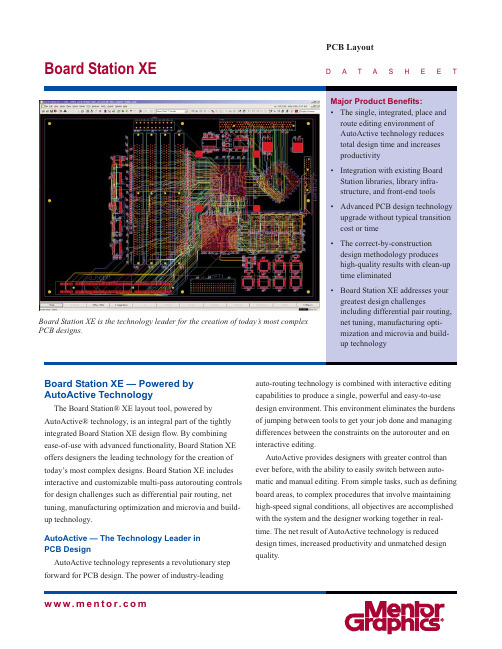
Board Station XEPCB LayoutD A T A S HE E Tw w w.m e n t o r.c o mBoard Station XE is the technology leader for the creation of today’s most complex PCB designs.Board Station XE — Powered by AutoActive TechnologyThe Board Station® XE layout tool, powered byAutoActive® technology, is an integral part of the tightly integrated Board Station XE design flow. By combining ease-of-use with advanced functionality, Board Station XE offers designers the leading technology for the creation of today’s most complex designs. Board Station XE includes interactive and customizable multi-pass autorouting controls for design challenges such as differential pair routing, net tuning, manufacturing optimization and microvia and build-up technology.AutoActive — The Technology Leader in PCB DesignAutoActive technology represents a revolutionary step forward for PCB design. The power of industry-leadingauto-routing technology is combined with interactive editing capabilities to produce a single, powerful and easy-to-use design environment. This environment eliminates the burdens of jumping between tools to get your job done and managing differences between the constraints on the autorouter and on interactive editing.AutoActive provides designers with greater control than ever before, with the ability to easily switch between auto-matic and manual editing. From simple tasks, such as defining board areas, to complex procedures that involve maintaining high-speed signal conditions, all objectives are accomplished with the system and the designer working together in real-time. The net result of AutoActive technology is reduced design times, increased productivity and unmatched design quality.What is AutoActive Technology?· A single, integrated, place and route editing environment that reducestotal design time and increasesproductivity·All physical rules and high-speed rules are maintained ·Correct-by-construction design that produces high-quality results withclean-up time eliminated ·Shape-based, true 45 degree routing ·The most advanced autorouting technology ever. Stop and start theautorouter at any time and all results will be correct-by-construction ·Dynamic clean-up of traces through the reduction of segments, preven-tion of acute angles and applicationof pad entry rulesDynamic Area FillsBoard Station XE automatically clears area fills around traces, vias and pads as the board is edited. Dynamic area fills are so fast, Board Station XE allows you to keep your area fillsturned on while you are doing all youredits. Moving a via pushes and shovesother vias, traces and area fills andconnectivity is automatically main-tained.Rules By AreaRules by area functionality greatlyimproves routing around BGAs andother fine-pitched parts. Rule areasrepresent complete rule sets that areobeyed by online and batch DRC and ininteractive and automatic routing. Ruleareas may be defined by layer and canbe assigned to any polygon, rectangle orcircle. Trace widths and clearancesautomatically change when traversinginto or out of the rule area. You mayalso change via sizes and spans in a rulearea to maximize route completion.Multiplow With Variable ViaPatternsBoard Station XE’s multiplow func-tionality allows you to simultaneouslyroute multiple nets, including differen-tial pairs, with true 45 degree routing. Itcan even handle routing through areasof staggered pins. Traces being routedwill push and shove the other vias andtraces out of the way and automaticallyclear area fills as needed. Changes canbe easily made to a variety of selectablevia patterns at the touch of a button,allowing enhanced flexibility forrouting into dense areas of a design.Dynamic Hazard ReviewDesign hazards are dynamicallydisplayed and may be individuallyselected and colored for easy identifica-tion. When a hazard is fixed, it isdynamically removed from the hazardlist.Leverages Legacy Board StationFlowBoard Station XE can be usedquickly and easily by existing BoardStation Layout customers. First, BoardStation XE uses the same libraries(geometries) as the legacy flow. BoardStation XE is integrated with he samefront-end tools and library managementsystem as the legacy tools. Finally,customers can easily import legacyBoard Station Layout designs intoBoard Station XE in order to start newdesigns from an existing one. This allgives customers access to the state-of-the-art layout environment using theirexisting library infrastructure and front-end tools.Board Station XE features market-leading technology for advanced interconnect.High-Speed Design with Board Station XEDesigners today are increasingly challenged by the need to manage signal quality in order to achieve system performance and reduce proto-type iterations. High-speed design with Board Station XE is an integrated part of the AutoActive design environment.Constraint DefinitionBoard Station XE handles an exten-sive set of constraints to meet high-speed performance requirements whether you’re routing interactively or automatically. A common constraint definition environment is shared between schematic capture and layout, allowing the evaluation of critical signals at any design stage. Constraints include same layer and adjacent layer differential pairs, controlled impedance, net scheduling and delay.Net TuningWhile routing interactively, graphic tuning aids are displayed for guidance. Nets modified out-of-tune during edits are automatically re-tuned. The Hazards dialog box dynamically updates as you edit nets, providing instant feedback relative to your constraints. Nets can also be tuned within an autoroute pass. Tuned nets are automatically maintained as you complete the design.Differential Pair RoutingRouting and editing differential pairs with Board Station XE is accomplished with speed and ease that will change your view of high-speed design. Pair spacing rules can be established by both layer and net class. If one trace is edited, the other trace in the pair auto-matically moves with it. Adjacent layerdifferential pair routing capabilities addanother valuable option for routing crit-ical signals on a dense PCB.Xtreme TechnologyPatented Xtreme design technologyenables up to 15 clients to operate on acommon database simultaneously tointeractively develop PCB layouts(XtremePCB) and perform complexmulti-process auto-routing (XtremeAR)while reducing cycle times by up to70%.Advanced InterconnectRoutingThe challenges and of advancedinterconnect are prevalent today withBGA, CSP, COB and DCA packagesincreasing board density. Build-up andmicrovia structures used in these boarddesigns further complicate routing.Board Station XE, powered byAutoActive technology, offers theleading technology for advanced inter-connect designs.Board Station XE supports the defi-nition of complex via structure rulesand the routing of microvia geometries,including comprehensive via-in-padrules. Via spans between any two layersare possible. By moving beyond tradi-tional laminate layer pairing, BoardStation XE facilitates the design ofbuild-up structures on laminate toenable escape patterns from dense, highpin count devices. Build-up areas typi-cally have a smaller clearance than thelaminate beneath them. Board StationXE can establish delay values andclearances per via span to address theseissues. Additionally, Board Station XEfeatures true 45 degree routing for BGAfanout and staggered connectors,enabling localized rule definition tofacilitate escape paths from dense areas. Board Station XE features powerful differential pair routing and net tuning capabilities for advanced high-speed design.MF-04-081025940-wTo learn more about how Board Station XE can improve your PCB layout process, call Mentor Graphics to schedule a complete product demonstra-tion or visit our web site at / for the latest product news.Copyright © 2007 Mentor Graphics Corporation.Mentor Graphics, Board Station and AutoActive are registered trademarks and Xtreme and FabLink are trademarks of Mentor Graphics Corporation.All other trademarks mentioned in this document are trademarks of their respective owners.Printed on RecycledPaperFabLink XE Pro IntegrationBoard Station XE is tightly inte-grated with the new FabLink XE Pro manufacturing data preparation tools FabLink XE Pro provides a stand alone panel creation and editing environment for creating manufacturing data at the panel level that operates on a panel design database. In addition, it provides additional board level functionality,including detailed data views, search-able PDF output, copper balancing,various data outputs and Gerber In/Drill In capabilities. Manufacturing Output Validation (MOV) quickly and easily identifies out of date manufacturing data compared to the design data.FabLink XE interacts with design data at three levels: ManufacturingPreparation, Manufacturing Output and Documentation.Operating System Requirements •Windows 2000 •Windows Server 2003•Windows XP Professional •Linux•Red Hat Enterprise 3(Server & Desktop) •Red Hat Enterprise 4(Server & Desktop) •Red Hat Enterprise 5(Server & Desktop)•SUSE Enterprise 9(Server & Desktop)•SUSE Enterprise 10 (Server & Desktop)•Sun Solaris 2.8, 2.9, 2.10, X86Corporate Headquarters Mentor Graphics Corporation 8005 SW Boeckman Road Wilsonville, OR 97070-7777Phone: 503.685.7000Fax: 503.685.1204Sales and Product Information Phone: 800.547.3000Silicon ValleyMentor Graphics Corporation 1001 Ridder Park DriveSan Jose, California 95131 USA Phone: 408.436.1500Fax: 408.436.1501North American Support Center Phone: 800.547.4303EuropeMentor Graphics Deutschland GmbH Arnulfstrasse 20180634 Munich GermanyPhone: +49.89.57096.0Fax: +49.89.57096.40Pacific RimMentor Graphics (Taiwan)Room 1603, 16FInternational Trade BuildingNo. 333, Section 1, Keelung Road Taipei, Taiwan, ROC Phone: 886.2.87252000Fax: 886.2.27576027JapanMentor Graphics Japan Co., Ltd.Gotenyama Hills7-35, Kita-Shinagawa 4-chome Shinagawa-Ku, Tokyo 140 JapanPhone: 81.3.5488.3033Fax: 81.3.5488.3021。
FTDI UMFT201XB、UMFT220XB 和 UMFT230XB 数据手册说明书

UMFT201XB, UMFT220XB and UMFT230XB DatasheetVersion 1.2Document Reference No.: FT_000506 Clearance No.: FTDI# 272 Future TechnologyDevices InternationalLtdDatasheetUMFT201XB, UMFT220XB,UMFT230XB BreakoutModulesUSB to I2C/UART/FT1248 breakout modules1IntroductionUMFT201XB, UMFT220XB, and UMFT230XB breakoutmodules utilize FTDI’s FT201XQ, FT220XQ, andFT230XQ chips, respectively, to convert USB to serial or parallel interfaces. . These modules support thefollowing popular interfaces:-UMFT201XB bridges from USB to I2C IC.-UMFT220XB bridges from USB to a user chosen, parallel bit interface, FTDI’s FT1248/SPI. Note: 2out of the 4 I/0 lines are available for this module.-UMFT230XB bridges from USB to UART IC. 1.1FeaturesThis module is a breakout board with a lowprofile. It converts USB2.0 Full-Speed to aserial interface and connects the serialsignals to a 2.54mm (0.1”) pitch 10pinfemale receptacle. The boards do not use aUSB connector, but instead the modulesplug directly into the USB host connectorand the pads of the PCB makes electricalcontact with the electrical contacts of theUSB connector.All serial interfaces on these modulesoperate at +3.3V voltage levels, however allI/Os are 5V tolerant.2Driver SupportRoyalty-Free VIRTUAL COM PORT (VCP) DRIVERS for:∙Windows 8 32,64-bit∙Windows 7 32,64-bit∙Windows Vista∙Windows XP 32,64-bit∙Windows XP Embedded∙Windows 4.2 , 5.0 and 6.0 ∙MAC OS OS-X∙Linux 3.0 and greater∙Android Royalty-Free D2XX Direct Drivers (USB Drivers + DLL S/W Interface):∙Windows 8 32,64-bit∙Windows 7 32,64-bit∙Windows Vista∙Windows XP 32,64-bit∙Windows XP Embedded∙Windows 4.2, 5.0 and 6.0∙MAC OS OS-X∙Linux 3.0 and greater∙AndroidThe drivers listed above are all available to download for free from . Various 3rd Party Drivers are also available for various other operating systems - visit for details.3Ordering InformationTable of Contents1Introduction (1)1.1Features (1)2Driver Support (1)3Ordering Information (2)4Signals and Configurations (4)4.1UMFT-XB Module Pin Outs (4)4.2Signal Descriptions (4)4.3UMFT201XB CN2 Signal Descriptions (5)4.4UMFT220XB CN2 Signal Descriptions (5)4.5UMFT230XB CN2 Signal Descriptions (6)4.6CBUS Signal Options (6)4.7Configuring the MTP ROM (7)5Module Dimensions (8)6IC Package Markings (8)7UMFT-XB-WE Module Wire Connections (9)7.1UMFT201XB-WE Wire Connections (9)7.2UMFT220XB-WE Wire Connections (10)7.3UMFT230XB-WE Wire Connections (10)8Module Circuit Schematics (11)8.1UMFT201XB Schematic (11)8.2UMFT220XB Schematic (11)8.3UMFT230XB Schematic (12)9Environmental Compliances (12)10Internal MTP ROM Configuration (13)11Contact Information (14)Appendix A - List of Figures and Tables (15)Appendix B: Revision History (16)4 Signals and ConfigurationsFor all three modules, CN1 connects directly to a USB host or HUB port, or can be connected to a USB extension cable. This connects the USB data signals, 5V USB Bus power and GND. When connecting these modules to a USB host or HUB the USB signal pads should be facing upwards, and when connecting to vertical connector the USB signal pad should be facing right. If the module is plugged in the wrong way, no contact will be made between PCB and HUB, no damage will occur from plugging the module in upside down.4.1UMFT-XB Module Pin Outs4.2 Signal Descriptions4.3UMFT201XB CN2 Signal Descriptions4.4UMFT220XB CN2 Signal Descriptions4.5UMFT230XB CN2 Signal Descriptions4.6CBUS Signal OptionsFor further information on CBUS options, please refer to the relevant x-chip datasheet.* PWREN# must be used with a 10kΩ resistor pull up.**When in USB suspend mode the outputs clocks are also suspended.***The number of CBUS pins available varies for the three different modules.4.7Configuring the MTP ROMThe IC on each of the modules contains an embedded MTP memory that can be used to specify the functions of the CBUS pins, the current drive on each signal pin, current limit for the USB bus and the descriptors of the device. For details on using the MTP ROM/EEPROM programming utility FT_PROG, please see the FT_PROG User Guide.When programming the MT memory please note:i)The Max Bus Power setting of the MTP ROM should specify the maximum current to be drawn fromthe USB host/hub when enumerated. For high-powered USB devices the current limit whenenumerated is between 100mA and 500mA, for low-powered USB devices the current limit is100mA.5Module DimensionsTolerance +/-0.1mm2.3Figure 5.1 UMFT-XB Module DimensionsThe UMFT201XB, UMFT220XB and UMFT230XB modules are mechanically identical. Figure 5.1 Uses UMFT230 to illustrate the mechanical details.6IC Package MarkingsThe date code format is YYXX where XX = 2 digit week number, YY = 2 digit year number. This is followed by the revision letter.The code XXXXXXX is the manufacturing LOT code.FTDIXXXXXXXXXXFT201XQ 51YYWW-D8127UMFT-XB-WE Module Wire Connections7.1 UMFT201XB-WE Wire ConnectionsBLACKBROWN RED ORANGE YELLOW GREEN GREY PURPLE BLUE WHITEFigure 7.1 UMFT201XB-WE Wire Connections (numbers refer to pad numbers on the PCB)Figure 6.1 illustrates the –WE product as a cable. This is only for illustration purposes. The wire ended product consists of individual wires – not a cable7.2 UMFT220XB-WE Wire ConnectionsBLACKBROWN RED ORANGE YELLOW GREEN GREY PURPLE BLUE WHITEFigure 7.2 UMFT220XB-WE Wire Connections (numbers refer to pad numbers on the PCB)Figure 6.2 illustrates the –WE product as a cable. This is only for illustration purposes. The wire ended product consists of individual wires – not a cable7.3UMFT230XB-WE Wire ConnectionsBLACKBROWN RED ORANGE YELLOW GREEN GREY PURPLE BLUE WHITEFigure 7.3 UMFT230XB-WE Wire Connections (numbers refer to pad numbers on the PCB)Figure 6.3 illustrates the –WE product as a cable. This is only for illustration purposes. The wire ended product consists of individual wires – not a cable8Module Circuit Schematics 8.1UMFT201XB SchematicFigure 8.1 UMFT201XB Circuit Schematic8.2UMFT220XB SchematicFigure 8.2 UMFT220XB Circuit Schematic8.3UMFT230XB SchematicFigure 8.3 UMFT230XB Circuit Schematic9Environmental CompliancesThe UMFT-XB modules exclusively use lead free components, and are fully compliant with European Union directive 2002/95/EC.10Internal MTP ROM ConfigurationFollowing a power-on reset or a USB reset the FT-X chips will scan its internal MTP ROM and read the USB configuration descriptors stored there. The default values programmed into the internal MTP ROM in the FT201/220/230XB modules is shown in Table 10.1.The internal MTP ROM in the FT-X chip can be programmed over USB using the utility program FT_PROG. FT_PROG can be downloaded from the . Users who do not have their own USB vendor ID but who would like to use a unique Product ID in their design can apply to FTDI for a free block of unique PIDs. Contact FTDI Support(*********************)forthisservice.11Contact InformationHead Office – Glasgow, UKUnit 1, 2 Seaward Place, Centurion Business Park Glasgow G41 1HHUnited KingdomTel: +44 (0) 141 429 2777Fax: +44 (0) 141 429 2758E-mail (Sales) *******************E-mail (Support) *********************E-mail (General Enquiries) ******************* Branch Office – Taipei, Taiwan2F, No. 516, Sec. 1, NeiHu RoadTaipei 114Taiwan , R.O.C.Tel: +886 (0) 2 8797 1330Fax: +886 (0) 2 8751 9737E-mail (Sales) **********************E-mail (Support) ************************ E-mail (General Enquiries) **********************Branch Office – Hillsboro, Oregon, USA 7130 SW Fir LoopTigard, OR 97223USATel: +1 (503) 547 0988Fax: +1 (503) 547 0987E-Mail (Sales) *********************E-Mail (Support) *********************** E-Mail (General Enquiries) *********************Branch Office – Shanghai, ChinaRoom 1103, No. 666 West Huaihai Road, Shanghai, 200052ChinaTel: +86 (0)21 6235 1596Fax: +86 (0)21 6235 1595E-mail (Sales) *********************E-mail (Support) *********************** E-mail (General Enquiries) *********************Web SiteDistributor and Sales RepresentativesPlease visit the Sales Network page of the FTDI Web site for the contact details of our distributor(s) and sales representative(s) in your country.System and equipment manufacturers and designers are responsible to ensure that their systems, and any Future Technology Devices International Ltd (FTDI) devices incorporated in their systems, meet all applicable safety, regulatory and system-level performance requirements. All application-related information in this document (including application descriptions, suggested FTDI devices and other materials) is provided for reference only. While FTDI has taken care to assure it is accurate, this information is subject to customer confirmation, and FTDI disclaims all liability for system designs and for any applications assistance provided by FTDI. Use of FTDI devices in life support and/or safety applications is entirely at the u ser’s risk, and the user agrees to defend, indemnify and hold harmless FTDI from any and all damages, claims, suits or expense resulting from such use. This document is subject to change without notice. No freedom to use patents or other intellectual property rights is implied by the publication of this document. Neither the whole nor any part of the information contained in, or the product described in this document, may be adapted or reproduced in any material or electronic form without the prior written consent of the copyright holder. Future Technology Devices International Ltd, Unit 1, 2 Seaward Place, Centurion Business Park, Glasgow G41 1HH, United Kingdom. Scotland Registered Company Number: SC136640Appendix A - List of Figures and TablesList of FiguresFigure 5.1 UMFT-XB Module Dimensions (8)Figure 7.1 UMFT201XB-WE Wire Connections (numbers refer to pad numbers on the PCB) (9)Figure 7.2 UMFT220XB-WE Wire Connections (numbers refer to pad numbers on the PCB) (10)Figure 7.3 UMFT230XB-WE Wire Connections (numbers refer to pad numbers on the PCB) (10)Figure 8.1 UMFT201XB Circuit Schematic (11)Figure 8.2 UMFT220XB Circuit Schematic (11)Figure 8.3 UMFT230XB Circuit Schematic (12)List of TablesTable 4.1 Module PinOut List (4)Table 4.2 CN1 PinOut Description (4)Table 4.3 I2C Module Pin Out Description (5)Table 4.4 FT1248 Module Pin Out Description (5)Table 4.5 UART Module Pin Out Description (6)Table 4.6 CBUS Configuration Control (7)Table 10.1 Default Internal MTP ROM Configuration (13)Appendix B: Revision HistoryDocument Title: UMFT201XB, UMFT220XB and UMFT230XBDocument Reference No.: FT_000506Clearance No.: FTDI# 272Product Page: /FT-X.htmDocument Feedback: Send FeedbackVersion 1.0 Initial Datasheet Created 09/02/12 Version 1.1 Updated Photos and added Window 8 to driver support list 31/01/13 Version 1.2 Updated -01 part number 03/07/2015。
Belling BL24C04F 4Kbits (512×8) 电子可编程可读存储器(EEPROM)
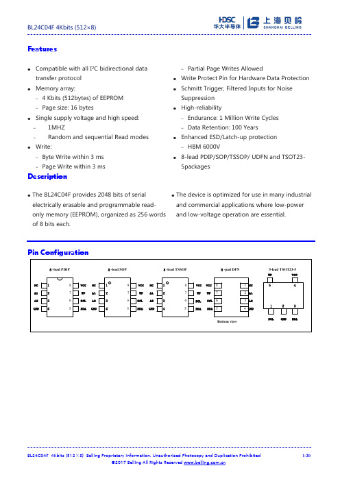
Features●Compatible with all I²C bidirectional datatransfer protocol●Memory array:– 4 Kbits (512bytes) of EEPROM–Page size: 16 bytes●Single supply voltage and high speed:–1MHZ–Random and sequential Read modes ●Write:–Byte Write within 3 ms–Page Write within 3 ms–Partial Page Writes Allowed●Write Protect Pin for Hardware Data Protection ●Schmitt Trigger, Filtered Inputs for NoiseSuppression●High-reliability–Endurance: 1 Million Write Cycles–Data Retention: 100 Years●Enhanced ESD/Latch-up protection–HBM 6000V●8-lead PDIP/SOP/TSSOP/ UDFN and TSOT23-5packagesDescription●The BL24C04F provides 2048 bits of serial electrically erasable and programmable read-only memory (EEPROM), organized as 256 words of 8 bits each. ●The device is optimized for use in many industrial and commercial applications where low-power and low-voltage operation are essential.Pin ConfigurationNC A1 A2 GNDVCCWPNCA1A2GNDNCA1A2GNDNCA1A2GNDVCCWPVCCWPVCCWP123487651234123487658765123487658-lead PDIP8-lead SOP8-lead TSSOP8-pad DFNBottem viewSCLSDASCLSDASCLSDASCLSDAWP VCCSCL SDAGND541235-lead TSOT23-5Pin DescriptionsTable 1Block DiagramFigure 1DEVICE/PAGE ADDRESSES (A2, A1 and A0): The A2, A1 and A0 pins are device address inputs that are hard wire for the BL24C04F. Eight 2K devices may be addressed on a single bus system (device addressing is discussed in detail under the Device Addressing section).SERIAL DATA (SDA): The SDA pin is bi-directional for serial data transfer. This pin is open-drain driven and may be wire-ORed with any number of other open-drain or open- collector devices.SERIAL CLOCK (SCL): The SCL input is used to positive edge clock data into each EEPROM device and negative edge clock data out of each device.WRITE PROTECT (WP):The BL24C04F has a Write Protect pin that provides hardware data protection. The Write Protect pin allows normal read/write operations when connected to ground (GND). When the Write Protection pin is connected to Vcc, the write protection feature is enabled and operates as shown in the following Table 2.Table 2Functional Description1.Memory OrganizationBL24C04F, 4K SERIAL EEPROM: Internally organized with 32 pages of 16 bytes each, the 4K requires a 9-bit data word address for random word addressing.2.Device OperationCLOCK and DATA TRANSITIONS: The SDA pin is normally pulled high with an external device. Data on the SDA pin may change only during SCL low time periods (see Figure 2). Data changes during SCL high periods will indicate a start or stop condition as defined below.START CONDITION: A high-to-low transition of SDA with SCL high is a start condition which must precede any other command (see Figure 3).STOP CONDITION: A low-to-high transition of SDA with SCL high is a stop condition. After a read sequence, the stop command will place the EEPROM in a standby power mode (see Figure 3).ACKNOWLEDGE: All addresses and data words are serially transmitted to and from the EEPROM in 8-bit words. The EEPROM sends a "0" to acknowledge that it has received each word. This happens during the ninth clock cycle.STANDBY MODE: The BL24C04F features a low-power standby mode which is enabled: (a) upon power-up and (b) after the receipt of the STOP bit and the completion of any internal operations.MEMORY RESET: After an interruption in protocol, power loss or system reset, any two-wire part can be reset by following these steps:1. Clock up to 9 cycles.2. Look for SDA high in each cycle while SCL is high.3. Create a start condition.BL24C04F 4Kbits (512×8)BL24C04F 4Kbits (512×8) Belling Proprietary Information. Unauthorized Photocopy and Duplication Prohibited4-20DATA STABLEDATA STABLEDATA CHANGESDASCLFigure 2. Data ValidityFigure 4. Output Acknowledge3.Device AddressingThe 4K EEPROM devices all require an 8-bit device address word following a start condition to enable the chip for a read or write operation (see Figure 5)MSB LSBFigure 5. Device AddressThe device address word consists of a mandatory "1", "0" sequence for the first four most significant bits as shown. This is common to all the Serial EEPROM devices.The 4K EEPROM uses A2 and A1 device address bits to allow as much as for devices on the same bus. These 2 bits must be compared to their corresponding hardwired input pins. The A2 and A1 pins use an internal proprietary circuit that biases them to a logic low condition if the pins are allowed to float.The eighth bit of the device address is the read/write operation select bit. A read operation is initiated if this bit is high and a write operation is initiated if this bit is low.Upon a compare of the device address, the EEPROM will output a "0". If a compare is not made, the chip will return to a standby state.DATA SECURITY: The BL24C04F has a hardware data protection scheme that allows the user to write protect the entire memory when the WP pin is at VCC.4.Write OperationsBYTE WRITE: A write operation requires an 9-bit data word address following the device address word and acknowledgment. Upon receipt of this address, the EEPROM will again respond with a "0" and then clock in the first 8-bit data word. Following receipt of the 8-bit data word, the EEPROM will output a "0" and the addressing device, such as a microcontroller, must terminate the write sequence with a stop condition. At this time the EEPROM enters an internally timed write cycle, tWR, to the nonvolatile memory. All inputs are disabled during this write cycle and the EEPROM will not respond until the write is complete (see Figure 7).MSB LSBFigure 6. ADDRESSSDA LINE STARTDEVICEADDRESSWRITEMSBLSBR/WACKADDRESSACKLSBACKLSBSTOPDATAFigure 7. Byte WritePAGE WRITE: The 4K EEPROM is capable of an 16-byte page write. A page write is initiated the same as a byte write, but the microcontroller does not send a stop condition after the first data word is clocked in. Instead, after the EEPROM acknowledges receipt of the first data word, the microcontroller can transmit up to seven more data words. The EEPROM will respond with a "0" after each data word received. The microcontroller must terminate the page write sequence with a stop condition (see Figure 8).ST A R TDEVICEADDRESSWRITEMSBLSBR/WACKADDRESSACKLSBACKLSBACKSTOPDATA(n)ACKDATA(n+1)DATA(n+1)SDALINEFigure 8. Page WriteThe data word address lower three bits are internally incremented following the receipt of each data word. The higher data word address bits are not incremented, retaining the memory page row location. When the word address, internally generated, reaches the page boundary, the following byte is placed at the beginning of the same page. If more than eight data words are transmitted to the EEPROM, the data word address will "roll over" and previous data will be overwritten.ACKNOWLEDGE POLLING: Once the internally timed write cycle has started and the EEPROM inputs are disabled, acknowledge polling can be initiated. This involves sending a start condition followed by the device address word. The read/write bit is representative of the operation desired. Only if the internal write cycle has completed will the EEPROM respond with a "0", allowing the read or write sequence to continue.5.Read OperationsRead operations are initiated the same way as write operations with the exception that the read/write select bit in the device address word is set to "1". There are three read operations: current address read, random address read and sequential read.CURRENT ADDRESS READ:The internal data word address counter maintains the last address accessed during the last read or write operation, incremented by one. This address stays valid between operations as long as the chip power is maintained. The address "roll over" during read is from the last byte of the last memory page to the first byte of the first page. The address "roll over" during write is from the last byte of the current page to the first byte of the same page. Once the device address with the read/write select bit set to "1" is clocked in and acknowledged by the EEPROM, the current address data word is serially clocked out. The microcontroller does not respond with an input "0" but does generate a following stop condition (see Figure 9).ST A R TDEVICEADDRESSREADMSBLSBR/WACKSTOPDATANOACKSDALINEFigure 9. Current Address ReadRANDOM READ: A random read requires a "dummy" byte write sequence to load in the data word address. Once the device address word and data word address are clocked in and acknowledged by the EEPROM, the microcontroller must generate another start condition. The microcontroller now initiates a current address read by sending a device address with the read/write select bit high. The EEPROM acknowledges the device address and serially clocks out the data word. The microcontroller does not respond with a "0" but does generate a following stop condition (see Figure 10)STA R TDEVICEADDRESSWRITEMSBLSBR/WACKNote.1*=DON'T CARE bitsADDRESSACKLSBSTOPDATA(n)DEVICEADDRESSSTARTREADACKNOACK DUMMY WRITESDALINEFigure 10. Random ReadSEQUENTIAL READ: Sequential reads are initiated by either a current address read or a random address read. After the microcontroller receives a data word, it responds with an acknowledge. As long as theEEPROM receives an acknowledge, it will continue to increment the data word address and serially clock out sequential data words. When the memory address limit is reached, the data word address will "roll over" and the sequential read will continue. The sequential read operation is terminated when the microcontroller does not respond with a "0" but does generate a following stop condition (see Figure 11).DEVICE ADDRESS READR/WACKACKACKACKSTOP DATA(n)DATA(n+1)DATA(n+2)DATA(n+x)NOACKSDALINEFigure 11. Sequential ReadElectrical CharacteristicsAbsolute Maximum Stress Ratings:●DC Supply Voltage . . . . . . . . . . . . . . . . . . . . . . . -0.3V to +6.5V●Input / Output Voltage . . . . . . . . . . . . . GND-0.3V to VCC+0.3V●Operating Ambient Temperature . . . . . . . . . . . . -40℃ to +85℃●Storage Temperature . . . . . . . . . . . . . . . . . . . . .-65℃ to +150℃●Electrostatic pulse (Human Body model) . . . . . . . . . . . . . 6000VComments:Stresses above those listed under "Absolute Maximum Ratings" may cause permanent damage to this device. These are stress ratings only. Functional operation of this device at these or any other conditions above those indicated in the operational sections of this specification is not implied or intended. Exposure to the absolute maximum rating conditions for extended periods may affect device reliability.DC Electrical CharacteristicsApplicable over recommended operating range from: TA = -40℃ to +85℃, VCC = +1.7V to +5.5V (unless otherwise noted)Pin CapacitanceApplicable over recommended operating range from TA = 25℃, f = 1.0 MHz, VCC = +1.7VAC Electrical CharacteristicsApplicable over recommended operating range from TA = -40℃ to +85℃, VCC = +1.8V to +5.5V, CL = 1 TTL Gate and 100 pF (unless otherwise noted)Bus TimingFigure 12. SCL: Serial Clock, SDA: Serial Data I/O Write Cycle TimingFigure 13. SCL: Serial Clock, SDA: Serial Data I/OPackage InformationPDIP Outline Dimensions1.This drawing is for general information only; refer to JEDEC Drawing MS-001, Variation BA for additional information.2. Dimensions A and L are measured with the package seated in JEDEC seating plane Gauge GS-3.3. D, D1 and E1 dimensions do not include mold Flash or protrusions. Mold Flash or protrusions shall not exceed 0.010 inch.4. E and eA measured with the leads constrained to be perpendicular to datum.5. Pointed or rounded lead tips are preferred to ease insertion.6. b2 and b3 maximum dimensions do not include Dambar protrusions. Dambar protrusions shall not exceed 0.010 (0.25 mm).Notes:These drawings are for general information only. Refer to JEDEC Drawing MS-012, Variation AA for proper dimensions, tolerances, datums, etc.1. This drawing is for general information only. Refer to JEDEC Drawing MO-153, Variation AA, for proper dimensions, tolerances, datums, etc.2. Dimension D does not include mold Flash, protrusions or gate burrs. Mold Flash, protrusions and gate burrs shall not exceed 0.15 mm (0.006 in) per side.3. Dimension E1 does not include inter-lead Flash or protrusions. Inter-lead Flash and protrusions shall not exceed 0.25 mm (0.010 in) per side.4. Dimension b does not include Dambar protrusion. Allowable Dambar protrusion shall be 0.08 mm total in excess of the b dimension at maximum material condition. Dambar cannot be located on the lower radius of the foot. Minimum space between protrusion and adjacent lead is 0.07 mm.5. Dimension D and E1 to be determined at Datum Plane H.Figure 17TSOT23-5Figure 18Marking DiagramPDIPBL24C04FYYWW#ZZSSSSSPYY: yearWW :weekZZ: assembly houseSSSSS : Lot IDSOPBL24C04FSSSSSP SSSSS : Lot IDTSSOPBL24C04FSSSSS SSSSS : Lot IDTSOT23-524C04FSSSSSP SSSSS : Lot IDOrdering InformationRevision history。
GE Industrial Solutions iVB Intelligent Embeded Po

• GB1984-2003
<High-voltage alternating current circuit breaker>
• GB/T11022-1999
Intelligent and Compact
Intelligence
Bring you reliable power solution
VCB is the most critical component for MV Switchgear iVB integrates conveniently for you
<Common specifications for high-voltage switchgear and control gear standards>
• DL/T 402-2007
<High-voltage alternating current circuit breakers>
• DL/T 403-2000
T : +86 21 3877 7888
Printing Code: IN201301B26EN
F : +86 21 3877 7600
© Copyright GE Industrial Solutions 2013
iVB Intelligent Embeded Pole Vacuum Circuit Breaker
Aux. contact
iTU
iTU Intelligent relay protection
OXuPCI954_DS

External—Free ReleaseOxford Semiconductor, Inc.1900 McCarthy Boulevard, Suite 210 © Oxford Semiconductor, Inc. 2007F EATURES• Four 16C950 High performance UART channels • 8-bit Pass-through Local Bus (PCI Bridge )• IEEE1284 Compliant SPP/EPP/ECP parallel port (with external transceiver)• Efficient 32-bit, 33 MHz, multi-function target-only PCIcontroller, fully compliant to PCI Local Bus Specification 3.0 and PCI Power Management Specification 1.1 • Software compatible with OXmPCI954• UARTs fully software compatible with 16C550-type devices • UART operation up to 60 MHz via external clock source. Up to 20 MHz with the crystal oscillator• Baud rates up to 60 Mbps in external 1x clock mode and 15 Mbps in asynchronous mode• 128-byte deep FIFO per transmitter and receiver • Flexible clock prescaler, from 1 to 31.875• Automated in-band flow control using programmable Xon/Xoff in both directions•Automated out-of-band flow control using CTS#/RTS# and/or DSR#/DTR#• Programmable RS485 turnaround delay• Arbitrary trigger levels for receiver and transmitter FIFO interrupts and automatic in-band and out-of-band flow control• Infra-red (IrDA) receiver and transmitter operation • 9-bit data framing, as well as 5, 6, 7, and 8 bits • Detection of bad data in the receiver FIFO• Global Interrupt Status and readable FIFO levels to facilitate implementation of efficient device drivers.• Local registers to provide status/control of device functions • 11 multi-purpose I/O pins, which can be configured as input interrupt pins or ‘wake-up’• Auto-detection of a wide range of optional MICROWIRE TM compatible EEPROMs, to re-configure device parameters • Function access , to pre-configure each function prior to handover to generic device drivers • Operation via I/O or memory mapping• 3.3 V or 5 V operation (PCI Universal Voltage)• Extended operating temperature range: -40° C to 85° C •176-pin LQFP packageD ESCRIPTIONThe OXuPCI954 is a single chip solution for PCI-based serial and parallel expansion add-in cards. It is a dual function PCI device, where function 0 offers four ultra-high performance OX16C950 UARTs, and function 1 is configurable either as an 8-bit local bus or a bi-directional parallel port.Each UART channel in the OXuPCI954 is the fastest available PC-compatible UART, offering data rates up to 15 Mbps and 128-byte deep transmitter and receiver FIFOs. The deep FIFOs reduce CPU overhead and allow utilization of higher data rates. Each UART channel is software compatible with the widely used industry-standard 16C550 devices (and compatibles), as well as the OX16C95x family of high performance UARTs. In addition to increased performance and FIFO size, the UARTs also provide the full set of OX16C95x enhanced features including automated in-band flow control, readable FIFO levels, etc.To enhance device driver efficiency and reduce interrupt latency, internal UARTs have multi-port features such as shadowed FIFO fill levels, a global interrupt source register and Good-Data Status, readable in four adjacent DWORD registers visible to logical functions in I/O space and memory space.Expansion of serial ports beyond four channels is possible using the 8-bit pass-through Local Bus function. This provides a general address/data bus and interrupt capability to a discrete UART part, such as the Oxford SemiconductorOX16C954. Other controllers could be used to provide capabilities beyond additional UART ports. The addressable space provided by the Local Bus can be increased up to 256 bytes, and divided into four chip-select regions. This flexible expansion scheme caters for cards with up to 20 serial ports using external 16C950, 16C954 or compatible devices, or composite applications such as combined serial and parallel port expansion cards. Serial port cards with up to 20 ports (or with 4 serial ports and a parallel port) can be designed without redefining any device or timing parameters.The parallel port is an IEEE 1284 compliant SPP/EPP/ECP parallel port that fully supports the existing Centronics interface. The parallel port can be enabled in place of the local bus. A n external bus transceiver is required for 5V parallel port operation if device is 3.3V sourced.For full flexibility, all the default configuration register values can be overwritten using an optional M ICROWIRE compatibleserial EEPROM. This EEPROM can also be used to provide function access to pre-configure devices on the local bus/parallel port, prior to any PCI configuration accesses and before control is handed to (generic) device drivers.The OXuPCI954 can be used to replace the OXmPCI954 in a PCI application where quad UARTs and a local bus/parallel port functionality are required.OXuPCI954 DATA SHEETIntegrated High Performance Quad UARTs,8-bit Local Bus/Parallel Port,3.3 V and 5 V (Universal Voltage) PCI Interface .Improvements of the OXuPCI954 over Discrete SolutionsHigher degree of integrationThe OXuPCI954 device offers four internal 16C950 high-performance UARTs and an 8-bit local bus or abi-directional parallel port.Multi-function deviceThe OXuPCI954 is a multi-function device to enable users to load individual device drivers for the internal serial ports, drivers for the peripheral devices connected to the local bus or drivers for the internal parallel port.Quad Internal OX16C950 UARTsThe OXuPCI954 device contains four ultra-high performance UARTs, which can increase driver efficiency by using features such as the 128-byte deep transmitter and receiver FIFOs, flexible clock options, automatic flow control, programmable interrupt and flow control trigger levels and readable FIFO levels. Data rates are up to 60 Mbps.Improved access timingAccess to the internal UARTs require zero or one PCI wait state. A PCI read transaction from an internal UART can complete within five PCI clock cycles and a write transaction to an internal UART can complete within four PCI clock cycles. Reduces interrupt latencyThe OXuPCI954 device offers shadowed FIFO levels and Interrupt status registers on the internal UARTs and the MIO pins. This reduces the device driver interrupt latency. Power managementThe OXuPCI954 device complies with the PCI Power Management Specification 1.1 and the Microsoft Communications Device-class Power Management Specification 2.0 (2000). Both functions offer the extended capabilities for Power Management. This achieves significant power savings by enabling device drivers to power down the PCI functions. For function 0, this is through switching off the channel clock, in power state D3. Wake-up (PME# generation) can be requested by either functions. For function 0, this is via the RI# inputs of the UARTs in the power-state D3 or any modem line and SIN inputs of the UARTs in power-state D2. For function 1, this is via the MIO[2] input.Optional EEPROMThe OXuPCI954 device can be reconfigured from an external EEPROM to the end-user’s requirements. However, this is not required in many applications as the default values are sufficient for typical applications. An overrun detection mechanism built into the EEPROM controller prevents the PCI system from ‘hanging’ due to an incorrectly programmed EEPROM.R EVISION H ISTORYRevision Modification May 2007 First publication.Sep 2007 Feature revision, including removal of D3coldT ABLE OF C ONTENTS1OXuPCI954 Device Modes (6)2Block Diagram (7)3Pin Information—176-Pin LQFP (8)3.1Mode ‘0’ Quad UARTs + 8-bit Local Bus (8)3.1.1Mode ‘1’ : Quad UARTs + Parallel Port (9)3.2Pin Descriptions (10)4Configuration and Operation (16)5PCI Target Controller (17)5.1Operation (17)5.2Configuration Space (17)5.2.1PCI Configuration Space Register Map (18)5.3Accessing Logical Functions (20)5.3.1PCI Access to Internal UARTs (21)5.3.2PCI Access to 8-bit Local Bus (22)5.3.3PCI Access to Parallel Port (22)5.4Accessing Local Configuration Registers (23)5.4.1Local Configuration and Control Register ‘LCC’ (Offset 0x00) (23)5.4.2Multi-purpose I/O Configuration Register ‘MIC’ (Offset 0x04) (24)5.4.3Local Bus Timing Parameter Register 1 ‘LT1’ (Offset 0x08) (26)5.4.4Local Bus Timing Parameter Register 2 ‘LT2’ (Offset 0x0C) (27)5.4.5UART Receiver FIFO Levels ‘URL’ (Offset 0x10) (28)5.4.6UART Transmitter FIFO Levels ‘UTL’ (Offset 0x14) (29)5.4.7UART Interrupt Source Register ‘UIS’ (Offset 0x18) (29)5.4.8Global Interrupt Status and Control Register ‘GIS’ (Offset 0x1C) (30)5.5PCI Interrupts (31)5.6Power Management (32)5.6.1Power Management of Function 0 (32)5.6.2Power Management of Function 1 (33)5.6.3Universal Voltage (34)5.7Unique Bar Option – for Function 0 (35)6Internal OX16C950 UARTs (36)6.1Operation – Mode Selection (36)6.1.1450 Mode (36)6.1.2550 Mode (36)6.1.3Extended 550 Mode (36)6.1.4750 Mode (36)6.1.5650 Mode (36)6.1.6950 Mode (37)6.2Register Description Tables (38)6.3UART Reset Configuration (41)6.3.1Hardware Reset (41)6.3.2Software Reset (41)6.4Transmitter and Receiver FIFOs (42)6.4.1FIFO Control Register ‘FCR’ (42)6.5Line Control and Status (43)6.5.1False Start Bit Detection (43)6.5.2Line Control Register ‘LCR’ (43)6.5.3Line Status Register ‘LSR’ (44)6.6Interrupts and Sleep Mode (45)6.6.1Interrupt Enable Register ‘IER’ (45)6.6.2Interrupt Status Register ‘ISR’ (46)6.6.3Interrupt Description (46)6.6.4Sleep Mode (47)6.7Modem Interface (47)6.7.1Modem Control Register ‘MCR’ (47)6.7.2Modem Status Register ‘MSR’ (48)6.8Other Standard Registers (48)6.8.1Divisor Latch Registers ‘DLL and DLM’ (48)6.8.2Scratch Pad Register ‘SPR’ (48)6.9Automatic Flow Control (49)6.9.1Enhanced Features Register ‘EFR’ (49)6.9.2Special Character Detection (50)6.9.3Automatic In-band Flow Control (50)6.9.4Automatic Out-of-band Flow Control (50)6.10Baud Rate Generation (51)6.10.1General Operation (51)6.10.2Clock Prescaler Register ‘CPR’ (51)6.10.3Times Clock Register ‘TCR’ (51)6.10.4External 1x Clock Mode (53)6.10.5Crystal Oscillator Circuit (53)6.11Additional Features (54)6.11.1Additional Status Register ‘ASR’ (54)6.11.2FIFO Fill Levels ‘TFL and RFL’ (54)6.11.3Additional Control Register ‘ACR’ (54)6.11.4Transmitter Trigger Level ‘TTL’ (55)6.11.5Receiver Interrupt. Trigger Level ‘RTL’ (55)6.11.6Flow Control Levels ‘FCL’ and ‘FCH’ (56)6.11.7Device Identification Registers (56)6.11.8Clock Select Register ‘CKS’ (56)6.11.9Nine-bit Mode Register ‘NMR’ (57)6.11.10Modem Disable Mask ‘MDM’ (57)6.11.11Readable FCR ‘RFC’ (58)6.11.12Good-data Status Register ‘GDS’ (58)6.11.13Port Index Register ‘PIX’ (58)6.11.14Clock Alteration Register ‘CKA’ (58)6.11.15RS485 Delay Enable ‘RS485_DLYEN’ (58)6.11.16RS485 Delay Count ‘RS485_DLYCNT’ (59)7Local bus (60)7.1Overview (60)7.2Operation (60)7.3Configuration and Programming (61)8Bidirectional Parallel Port (62)8.1Operation and Mode Selection (62)8.1.1SPP Mode (62)8.1.2PS2 Mode (62)8.1.3EPP Mode (62)8.1.4ECP Mode (62)8.2Parallel Port Interrupt (63)8.3Register Description (63)8.3.1Parallel Port Data Register ‘PDR’ (64)8.3.2ECP FIFO Address / RLE (64)8.3.3Device Status Register ‘DSR’ (64)8.3.4Device Control Register ‘DCR’ (64)8.3.5EPP Address register ‘EPPA’ (65)8.3.6EPP Data Registers ‘EPPD1-4’ (65)8.3.7ECP Data FIFO (65)8.3.8Test FIFO (65)8.3.9Configuration A Register (65)8.3.10Configuration B Register (65)8.3.11Extended Control Register ‘ECR’ (65)9Serial EEPROM (66)9.1Specification (66)9.1.1Zone 0: Header (67)9.1.2Zone 1: Local Configuration Registers (68)9.1.3Zone 2: Identification Registers (69)9.1.4Zone 3: PCI Configuration Registers (69)9.1.5Zone 4: Power Management DATA (and DATA_SCALE Zone) (70)9.1.6Zone 5: Function Access (70)10Operating Conditions (72)10.1DC Electrical Characteristics (72)11AC Electrical Characteristics (76)11.1PCI Bus Timings (76)11.2Local Bus (77)11.3Serial Ports (79)12Timing Waveforms (80)13Package Information (95)13.1176-Pin LQFP (95)14Ordering Information (96)1OX U PCI954D EVICE M ODESThe OXuPCI954 supports two modes of operation. These modes are summarized in the following table.Device Mode Mode Pin Selection Functionality0 MODE = 0 Function 0 : Quad UARTs Function 1 : 8-bit local bus1 MODE = 1 Function 0 : Quad UARTs Function 1 : Parallel Port* The OXuPCI954 is not pin-compatible with the OX16PCI954 or the OXmPCI954, but is the same in all other aspects.2B LOCK D IAGRAMFIFOSELMODEAD[31:0]C/BE[3:0]#PCI_CLKFRAME#DEVSEL#IRDY#TRDY#STOP#PARPERR#IDSELRST#INTA#PME#XTLIXTLOUART_Clk_Out Local_Bus ClkEE_DIEE_CSEE_CKEE_DOSOUT[3:0]SIN[3:0]RTS[3:0]DTR[3:0]CTS[3:0]DSR[3:0]DCD[3:0]RI[3:0]MIO[10:0]PD[7:0]ACK#PEBUSYSLCTERR#SLIN#INIT#AFD#STB#LBA[7:0]LBD[7:0]LBCS[3:0]LBWR#LBRD#LBRSTDATA_DIR OXuPCI954 Block DiagramOSCDIS XTLSEL3P IN I NFORMATION—176-P IN LQFP 3.1Mode ‘0’ Quad UARTs + 8-bit Local Bus7 NC. Do not connect these pins:23, 40, 41, 136, 137, 138, 1393.1.1Mode ‘1’ : Quad UARTs + Parallel Port15 NC. Do not connect these pins:23, 40, 41, 74, 112, 113, 114, 115, 116, 117, 124, 136, 137, 138, 1393.2Pin DescriptionsFor the actual pinouts of the OXuPCI954 device (for the various modes), refer to the Section 3, Pin Information. The I/O direction key table is on page 15.PCI Interface – All ModesPin Dir1Name Description149, 150, 151, 154, 155,157, 158, 160, 164, 165,167, 168, 169, 170, 171,174, 13, 14, 15, 17, 18, 20,24, 25, 27, 28, 31, 32, 33,34, 35, 39P_I/O AD[31:0] Multiplexed PCI Address/Data bus161, 175, 12, 26 P_I C/BE[3:0]# PCI Command/Byte enable146 P_I CLK PCI system clock (33MHz)176 P_IFRAME#CycleFrame5 P_ODEVSEL#DeviceSelect1 P_IIRDY#Initiatorready2 P_OTRDY#Targetready6 P_O STOP# Target Stop request10 P_I/OPAR Parity8 P_OSERR#Systemerror7 P_I/OPERR#Parityerror163 P_I IDSEL Initialization device select144 P_I RST# PCI system reset142 P_ODINTA# PCIinterrupt147 P_OD PME# Power management eventSerial Port Pins – All ModesPin Dir1Name Description50 I FIFOSEL FIFO select. For backward compatibility with 16C550,16C650 and 16C750 devices the UARTs’ FIFO depth is 16when FIFOSEL is low. The FIFO size is increased to 128when FIFOSEL is high. The unlatched state of this pin isreadable by software. The FIFO size may also be set to 128by setting FCR[5] when LCR[7] is set, or by putting thedevice into Enhanced mode.82, 81, 63, 62 O(h)SOUT[3:0]IrDA_Out[3:0] These four pins are present in all modes but they can serve one of two functions, as follows:UART serial data outputs.UART IrDA data output when MCR[6] of the corresponding channel is set in Enhanced mode.91, 73, 72, 55I(h) I(h) SIN[3:0]IrDA_In[3:0]These four pins are present in all modes but they can serveone of two functions, as follows:UART serial data inputs.UART IrDA data input when IrDA mode is enabled (seeabove).Serial Port Pins – All ModesPin Dir1Name Description89, 76, 71, 57 I(h) DCD[3:0]# Active-low modem data-carrier-detect input 84, 79, 65, 60O(h) O(h) O(h) DTR[3:0]#485_En[3:0]Tx_Clk_Out[3:0]These four pins are present in all modes but they can serveone of three functions, as follows:Active-low modem data-terminal-ready output. If automatedDTR# flow control is enabled, the DTR# pin is asserted anddeasserted if the receiver FIFO reaches or falls below theprogrammed thresholds, respectively.In RS485 half-duplex mode, the DTR# pin may beprogrammed to reflect the state of the transmitter empty bitto automatically control the direction of the RS485transceiver buffer (see register ACR[4:3]).Transmitter 1x clock (baud rate generator output). Forisochronous applications, the 1x (or Nx) transmitter clockmay be asserted on the DTR# pins (see register CKS[5:4]).83, 80, 64, 61 O(h) RTS[3:0]# Active-low modem request-to-send output. If automatedRTS# flow control is enabled, the RTS# pin is deassertedand reasserted whenever the receiver FIFO reaches or fallsbelow the programmed thresholds, respectively.85, 78, 67, 59 I(h) CTS[3:0]# Active-low modem clear-to-send input. If automated CTS#flow control is enabled, upon deassertion of the CTS# pin,the transmitter will complete the current character and enterthe idle mode until the CTS# pin is reasserted. Note: any in-band flow control characters are transmitted regardless ofthe state of the CTS# pin.86, 77, 66, 58I(h) I(h) DSR[3:0]#Rx_Clk_In[3:0]These four pins are present in all modes but they can serveone of two functions, as follows:Active-low modem data-set-ready input. If automated DSR#flow control is enabled, upon deassertion of the DSR# pin,the transmitter will complete the current character and enterthe idle mode until the DSR# pin is reasserted. Note: any in-band flow control characters are transmitted regardless ofthe state of the DSR# pin.External receiver clock for isochronous applications. TheRx_Clk_In is selected when CKS[1:0] = ‘01’.90, 75, 70, 56 I(h)I(h) RI[3:0]#Tx_Clk_In[3:0]Active-low modem Ring-Indicator inputExternal transmitter clock. This clock can be used by thetransmitter (and indirectly by the receiver) when CKS[6]=’1’.Clock Interface Pins – All ModesPin Dir 1 Name Description49 I/OXTLOCrystal oscillator output when OSCDIS = ‘0’.External clock source input when OSCDIS = ‘1’48 I XTLI Crystal oscillator input when OSCDIS = ‘0’, up to 20MHz.N/C when OSCDIS = ‘1’45 I OSCDIS Oscillator disable.When 0, the internal crystal oscillator is enabled and a crystal needs to be attached to XTLI/XTLO.XTLSEL must be set according to the crystal frequency that is used (up to 20Mhz).When 1, the internal crystal oscillator is disabled and an external oscillator source (up to 60MHz) can be input to XTLO. XTLI is N/C and XTLSEL must be 0130 I XTLSEL Defines the frequency of the crystal attached to XTLI/XTLO(when OSCDIS = ‘0’)0 = 1 MHz – 12 MHz 1 = 12 MHz – 20 MHz8-bit Local Bus – Mode 0Pin Dir 1 Name Description 111O UART_CLK_Out Buffered crystal output. This clock can drive external UARTsconnected to the local bus. Can be enabled / disabled by software.123 O(h) LBRST Local bus active-high reset. 124 O LBRST# Local bus active-low reset. 104 O LBDOUT Local bus data out enable. This pin can be used by externaltransceivers; it is high when LBD[7:0] are in output mode and low when they are in input mode.74 O LBCLK Buffered PCI clock. Can be enabled / disabled by software. 114, 115, 116, 117 O(h) O(h) LBCS[3:0]# LBDS[3:0]# Local bus active-low Chip-Select (Intel mode).Local bus active-low Data-Strobe (Motorola mode).112 O O LBWR# LBRDWR# Local bus active-low write-strobe (Intel mode).Local bus Read-not-Write control (Motorola mode).113 O Z LBRD# Hi-Z Local bus active-low read-strobe (Intel mode).Permanent high impedance (Motorola mode).105, 106, 108, 109 118, 119, 120, 122 O(h) LBA[7:0] Local bus address signals. 96, 97, 98, 99 100, 101, 102, 103I/O(h) LBD[7:0] Local bus data signals.Parallel Port – Mode 1Pin Dir 1 NameDescription123 I(h) I(h) ACK#INTR#Acknowledge (SPP mode). ACK# is asserted (low) by the peripheral to indicate that a successful data transfer has taken place.Identical function to ACK# (EPP mode).122 I(h) PEPaper Empty. Activated by printer when it runs out of paper. 120 I(h) I(h) BUSYWAIT#Busy (SPP mode). BUSY is asserted (high) by the peripheral when it is not ready to accept data.Wait (EPP mode). Handshake signal for interlocked IEEE 1284 compliant EPP cycles.109 OD(h) O(h) SLIN#ADDRSTB#Select (SPP mode). Asserted by host to select the peripheral.Address strobe (EPP mode) provides address read and write strobe.119 I(h) SLCT Peripheral selected. Asserted by peripheral when selected. 118 I(h) ERR#Error. Held low by the peripheral during an error condition. 108 OD(h) O(h) INIT#INIT#Initialize (SPP mode). Commands the peripheral to initialize.Initialize (EPP mode). Identical function to SPP mode. 106 OD(h) O(h) AFD#DATASTB# Auto Feed (SPP mode, open-drain).Data strobe (EPP mode) provides data read and write strobe.105 OD(h) O(h) STB#WRITE#Strobe (SPP mode). Used by peripheral to latch data currently available on PD[7:0].Write (EPP mode). Indicates a write cycle when low and a read cycle when high . 96, 97, 98, 99, 100, 101, 102, 103I/O(h) PD[7:0] Parallel data bus.104OPDOUTParallel port data out enable. This pin should be used by external transceivers for 5 V signaling; it is high when PD[7:0] are in output mode and low when they are in input mode.Multi-purpose and External Interrupt Pins – All ModesPin Dir1Name DescriptionMODE0 1135 --135I/O(h)OMIO0NCMulti-purpose I/O 0. Can drive high or low, or assert a PCIinterrupt.Output Driving ‘0’. Can be left as a No-connect.134 134 134134I/O(h)MIO1NCMulti-purpose I/O 1. Can drive high or low, or assert a PCIinterrupt (as long as LCC[6:5] = “00”).Output Driving ‘0’ (when LCC[6:5] ≠ ‘00’)Can be left as a No-Connect.133 133 133133I/O(h)IMIO2PME_InMulti-purpose I/O 2. When LCC[7] = 0, this pin can drive highor low, or assert a PCI interrupt.Input power management event. When LCC[7] is set thisinput pin can assert a function 1 PME#.93, 94, 95, 125, 126, 127, 128, 132 I/O(h) MIO[10:3] Multi-purpose I/O pins. Can drive high or low, or assert a PCIinterrupt.EEPROM Pins – All ModesPin Dir1Name Description53 OEE_CKEEPROMclock.52 O EE_CS EEPROM active-high Chip Select.54 IU(h) EE_DI EEPROM data in, with internal pull-up.When the serial EEPROM is connected, this pin should bepulled up using a 1-10k resistor. When the EEPROM is notused the internal pull-up is sufficient.Pin to be connected to the external EEPROM’s EE_DO pin(if used).51 O EE_DO EEPROM data out.Pin to be connected to the external EEPROM’s EE_DI pin(if used).Table 1: Pin DescriptionsI/O Direction Key P_I PCI input 3.3 V Only P_O PCI output / PCITristates 3.3 V Only P_I/O PCI bi-directional 3.3 V Only P_OD PCI open drain 3.3 V OnlyI Input LVTTL level I(h) Input LVTTL level, 5 V tolerant IU(h) Input with internal pull-up LVTTL level, 5 V tolerant I/O(h) Bi-Directional LVTTL level, 5 V tolerantO Output Standard Output O(h) Output 5 V tolerant (High Voltage BI-Direct in output mode) OD Open drain Standard Open-drain Output OD(h) Open drain 5 V tolerant (High Voltage BI-Direct in open-drain mode) NC No connectG Ground V VoltageMiscellaneous PinsPin Dir 1 NameDescription44 IMODEMode selector Pin0 : Function 0 : Quad UART. Function 1 : 8-bit local bus.1 : Function 0 : Quad UART. Function 1 : Parallel port.Power and GroundPinType Name Description19, 42, 47, 69, 88, 107, 131, 148VVDDPower Supply (3.3 V)11, 22, 36, 140, 156, 162, 173 V VIOPCI I/O Universal VoltageDefines the (clamping) voltage of the PCI I/O Buffers.To be connected to the VIO pin of the PCI connector. 3, 4, 9, 16, 21, 29, 30, 37, 38, 43, 46, 68, 87, 92, 110, 121, 129, 141, 143, 145, 152, 153, 159, 166, 172G GNDPower Supply Ground (0 V)4C ONFIGURATION AND O PERATIONThe OXuPCI954 is a multi-function, target-only PCI device, compliant with the PCI Local Bus Specification, Revision 3.0 and the PCI Power Management Specification, Revision 1.1.The OXuPCI954 affords maximum configuration flexibility by treating the internal UARTs, the local bus and the parallel port as separate logical functions. Each function has its own configuration space and is therefore recognized and configured by the PCI BIOS separately. The functions used are configured by the Mode Selection Pin as shown in Section 1 OXuPCI954 Device Modes.The OXuPCI954 is configured by system start-up software during the bootstrap process that follows bus reset. The system scans the bus and reads the vendor and device identification codes from any devices it finds. It then loads device-driver software according to this information and configures the I/O, memory and interrupt resources. Device drivers can then access the functions at the assigned addresses in the usual fashion, with the improved data throughput provided by PCI.Each function operates as though it was a separate device. However there are a set of Local Configuration Registers that can be used to enable signals and interrupts, configure timings, and improve the efficiency of multi-port drivers. This architecture enables separate drivers to be installed for each function. Generic port drivers can be hooked to use the functions individually, or more efficient multi-port drivers can hook both functions, accessing the Local Configuration Registers from either.All registers default after reset to suitable values for typical applications such a 4/8 port serial, or combo 4-port serial/1-port parallel add-in cards. However, all identification, control and timing registers can be redefined using an optional serial EEPROM.5PCI T ARGET C ONTROLLER5.1OperationThe OXuPCI954 responds to the following PCI transactions:-•Configuration access: The OXuPCI954 responds to type 0 configuration reads and writes if the IDSELsignal is asserted and the bus address is selecting theconfiguration registers for function 0 or 1. The devicewill respond to the configuration transaction by asserting DEVSEL#. Data transfer then follows. Anyother configuration transaction will be ignored by theOXuPCI954.•I/O reads/writes: The address is compared with the addresses reserved in the I/O Base Address Registers(BARs). If the address falls within one of the assignedranges, the device will respond to the I/O transactionby asserting DEVSEL#. Data transfer follows thisaddress phase. For the UARTs and 8-bit local buscontroller, only byte accesses are possible. For I/Oaccesses to these regions, the controller comparesAD[1:0] with the byte-enable signals as defined in thePCI specification. The access is always completed;however if the correct BE signal is not present thetransaction will have no effect.•Memory reads/writes: These are treated in the same way as I/O transactions, except that the memoryranges are used. Memory access to single-byte regions is always expanded to DWORDs in theOXuPCI954. In other words, OXuPCI954 reserves aDWORD per byte in single-byte regions. The deviceallows the user to define the active byte lane usingLCC[4:3] so that in Big-Endian systems the hardwarecan swap the byte lane automatically. For Memorymapped access in single-byte regions, the OXuPCI954 compares the asserted byte-enable withthe selected byte-lane in LCC[4:3] and completes theoperation if a match occurs, otherwise the access willcomplete normally on the PCI bus, but it will have noeffect on either the internal UARTs or the local buscontroller.•All other cycles (64-bit, special cycles, reserved encoding etc.) are ignored.The OXuPCI954 will complete all transactions as disconnect-with-data, i.e. the device will assert the STOP# signal alongside TRDY#, to ensure that the Bus Master does not continue with a burst access. The exception to this is Retry, which will be signaled in response to any access while the OXuPCI954 is reading from the serial EEPROM.The OXuPCI954 performs medium-speed address decoding as defined by the PCI specification. It asserts the DEVSEL# bus signal two clocks after FRAME# is first sampled low on all bus transaction frames which address the chip. The internal UARTs are accessed with zero wait states inserted. Fast back-to-back transactions are supported by the OXuPCI954 as a target, so a bus master can perform faster sequences of write transactions to the UARTs or local bus when an inter-frame turn-around cycle is not required.The device supports any combination of byte-enables to the PCI Configuration Registers and the Local Configuration Registers. If a byte-enable is not asserted, that byte is unaffected by a write operation and undefined data is returned upon a read.The OXuPCI954 performs parity generation and checking on all PCI bus transactions as defined by the standard. Note this is entirely unrelated to serial data parity which is handled within the UART functional modules themselves. If a parity error occurs during the PCI bus address phase, the device will report the error in the standard way by asserting the SERR# bus signal. However if that address/command combination is decoded as a valid access, it will still complete the transaction as though the parity check was correct.The OXuPCI954 does not support any kind of caching or data buffering in addition to that already provided within the UARTs by the transmit and receive data FIFOs. In general, registers in the UARTs and on the local bus can not be pre-fetched because there may be side-effects on read.5.2Configuration SpaceThe OXuPCI954 is a dual-function device, where each logical function has its own configuration space. All required fields in the standard header are implemented, plus the Power Management Extended Capability register set. The format of the configuration space is shown in the following tables.In general, writes to any registers that are not implemented are ignored, and all reads from unimplemented registers return 0.。
Extech CD Regulated Power Supply Modelos 382203 y

Manual del usuarioFuente de poder CD regulada con tres salidas Modelos 382203 (Análogo) y 382213 (Digital)IntroducciónFelicitaciones por seleccionar la Fuente de poder CD regulado Modelos 382203 (análogo) o 382213 (digital) de Extech. Los modelos 382203 y 382213 son fuentes de poder reguladas de estado sólido y compactos, apropiadas para muchas aplicaciones incluyendo pruebas de banco, servicio de campo, equipo de telecomunicaciones y diversión.Descripción del medidor1. Pantallas LCD Voltaje y Corriente2. LED indicador de estado de límite de corriente3. Interruptor de encendido con LED de estado4. Terminales de salida 5V y 12V fijo5. Terminales de salida alimentación variable6. Perillas de ajuste de voltaje y corriente variableNota: El Modelo 382213 (escalas LCD) se muestra arriba. El Modelo 382203 (mostrado en la portada) usa escala análoga.Operación1. La Fuente de poder debe ser alimentada con voltaje de línea nominal (110V ó 220V) dentro de+ 5%.2. Antes de encender, retire todas las cargas conectadas y fije la perilla de ajuste de voltajetotalmente contrarreloj (salida 0V CD).3. Para operar la fuente de alimentación como fuente de corriente constante, la salida de corrientedebe fijarse entre 10% y 100% del valor nominal (3A). El indicador de limitación de corriente se iluminará al activarse el circuito limitador de corriente.4. Use las perillas para ajuste de corriente y voltaje para fijar las salidas variables de corriente yvoltaje respectivamente. Use las terminales de salida variable para conexiones.5. Para las salidas de 5VCD y 12VCD, use las terminales de salida fija.6. Las pantallas análoga o digital indicaran las salidas reales de corriente y voltaje.7. Mantenga libre de obstrucciones las rejillas de ventilación del medidor (arriba y lados) paraprevenir sobrecalentamiento.Especificaciones382203382213Indicador Análogo doble conescalas Pantalla LCD doble de 3dígitosSalida de voltaje, CD0-30VSalida de corriente, CD0 - 3 amperiosIndicador de límite decorrienteLED de estadoPrecisión ± 7% de la escala total ± 1% de la escala total + 2dígitosOndulación y Ruido< 5mVRegulación de línea< 0,05% + 10mVVoltaje fijo de salida5V / 0,5A (Continuo); 1A (máx.)12V / 0,5A (Continuo); 1A (máx.)Tensión110/220VCA 50/60Hz (conmutable) Dimensiones152 x 142 x 242mm(6 x 5,6 x 9,5") (WxHxD)Peso4,5 kg (10 lbs.)Copyright (c)2012 Extech Instruments Corporation (a FLIR company) Reservados todos los derechos, incluyendo el derecho de reproducción total o parcial en cualquier medi o.。
温度传感器设置参数指南说明书

Cód.ParámetroU.M.TipoMín.Máx.VALOR/2Estabilidad de la medida -C 1154/3Deceleración visualización sonda-C 0150/4Sonda virtual-C 01000/5Selección °C o °F (0=°C, 1=°F)flag C 010/6Punto decimal (0=si 1=no)flag C 011/tI Visualización sobre el display -C 171/tE Visualización en terminal externo-C 060/P Selección tipo de sonda -C 020/A2Configuración de la sonda 2-C 042/A3Configuración de la sonda 3-C 040/A4Configuración de la sonda 4-C 040/A5Configuración de la sonda 5-C 040/c1Calibración de la sonda 1°C/°F C -20200/c2Calibración de la sonda 2°C/°F C -20200/c3Calibración de la sonda 3°C/°F C -20200/c4Calibración de la sonda 4°C/°F C -20200/c5Calibración de la sonda 5°C/°FC-2020St Set point (punto de consigna)°C/°F F r1r2-23rd Diferencial regulador°C/°F F 0.120 3.0rn Zona neutra°C/°F C 0604rr Diferencia inverso para control con zona neutra°C/°F C 0,1202r1SET mínimo admitido °C/°F C -50r2-23r2SET máximo admitido °C/°F C r120020TABLA DE PARÁMETROSCAREL: PUIFI0006 (MEMBRANA / ARMARIOS BT)/ PARÁMETROS SONDAr PARÁMETROS REGULADORr3Modalidad de funcionamientoflag C 020r4Variación automática del SET POINT nocturno °C/°F C -20200r5Habilitación de la monitorización de la temp.flag C 011rt Intervalo de monitorización de la temperaturahoras F 09990rH Máxima temperatura leída °C/°F F 000rLMínima temperatura leída°C/°FFc0Ret. arr. comp. y vent. en el mom. del encendido min C 0151c1Tiempo mínimo entre encendidos sucesivos min C 0151c2Tiempo mínimo de OFF del compresor min C 0150c3Tiempo mínimo de ON del compresormin C 0150c4Arranque forzado min C 01000cc Duración del ciclo continuohoras C 0150c6Tiempo exclusión de alarma después del ciclo continuohoras C 02502c7Tiempo máximo de Pump-Downs C 09000c8Retr. arr. comp. después de la ap. de la válvula PD s C 0605c9Habilitación función de autoarranque con func. en PDflag C 010c10Selección Pump-Down de tiempo o presiónflag C 010c11Retraso 2º compresorsC250d0Tipo de desescarche (0=resis. 1=gas 2=agua 3=gas a tiempo)flag C 041dI Intervalo entre dos desescarches horas F 02503dt1Temperatura fin desescarche evaporador °C/°F F -5020020dt2Temperatura fin desescarche evaporador auxiliar°C/°F F -5020020dt3Temperatura fin desescarche sonda 3°C/°F F -502004dP1Duración máx. del desescarche evaporador min F 125030dP2Duración máx. del desescarche evap. auxiliar min F 125030d3Retraso de activación del desescarche min C 02500d4Desescarche a la conexión del equipo flag C 010d5Retraso del desescarche a la conexion min C 02500d6Bloqueo del display durante el desescarche -C 021ddTiempo de goteo después del desescarcheminF154c PARÁMETROS COMPRESORd PARÁMETROS DE DESESCARCHEd8Exclusión alarmas después del desescarche horas F 02501d8d Tiempo exclusión de alarma tras puerta abierta min C 02500d9Prioridad del desescarche frente protecciones compresorflag C 010d/1Visualización de la sonda de desescarche °C/°F F 000d/2Visualización de la sonda de desescarche °C/°F F 000dC Base de los tiempos para desescarche flag C 010dC1Base de los tiempos para retardo de alarmas flag C 010d10Tiempo de funcionamiento del compresor min C 02500d11Umbral de temperatura para tiempo de funcionamiento°C/°F C -2020 1.0d12Desescarches avanzados -C 030dn Duración nominal del desescarche -C 110065dHFactor proporcional variación de ‘dI’-C10050A0Diferencial alarmas y ventiladores°C/°F C 0.120 1.0A1Tipo de umbral ‘AL’ y ‘AH’flag C 010AL Umbral de alarma de baja temperatura °C/°F F -5020010AH Umbral de alarma de alta temperatura °C/°F F -5020010Ad Retraso alarma baja y alta temperatura min F 0250120A4Configuración de la entrada digital 1-C 0120A5Configuración de la entrada digital 2-C 0120A6Bloqueo del compresor por alarma externa min C 01000A7Retraso de detección alarma externa min C 02500A8Habilitación alarmas ‘Ed1’ y ‘Ed2’ flag C 010A9Configuración salida digital 3flag C 0140Ado Configuración modo luz puerta flag C 010Ac Alarma alta temperatura del condensador °C/°F C 0.020070.0AE Difer. de la alarma de alta temp. cond.°C/°F C 0.12010Acd Retraso alarma alta temp. del condensadormin C 02500AF Tiempo apagado con sensor de luzseg C 02500ALF Umbral de alarma antihielo °C/°F C -50200-5AdFRetardo alarma antihielosegC250A PARÁMETROS DE ALARMAF0Control ventiladorflag C 022F1Temperatura encendido ventilador °C/°F F -50200 5.0F2Ventilador OFF con compresor OFFflag C 011F3Ventiladores en desescarche flag C 011Fd Ventiladores apagados después del goteo flag F 0150F4Temperatura ventilador condensador OFF°C/°F C -5020040F5Diferencial ventilador condensador°C/°FC0,1205Pw Contraseña -C 020022H0Dirección serial -C 02071H1Funcionalidad del relé 4flag C 0133H2Deshabilitación teclado/Infrared flag C 061H3Código habilitación telecomando -C 02550H4Deshabilitación zumbador flag C 010H5Funcionalidad del relé 5-C 0133H6Bloqueo teclas -C 025532H7Selección tecladoflag C 010H8Luz o salida aux conmutada con control horario-C 010H9Variación set point con control horario-C 010HPr Perfil de impresión-C 0150Hdn Num conjuntos de parámetros predeterminados disponibles-C 060Hdh Desfase de resistencia antivaho°C/°F C -502000HrL Control remoto de estado de relé de luz principal -C 010HrA Control remoto de estado de relé AUX principal -C 010HSA Control remoto de alarmas de controladores en ud principal-C 010In Tipo de unidad-C 060s_cLrH Orden baja humedad relativa-C 010s_cAUX Orden activar AUX -C 010s_cLUX Orden activar luz -C 010s_cONOFFOrden controlador ON/OFF-C1F PARÁMETROS VENTILADOR (solo para el modelo C)H OTRAS PREDISPOSICIONES。
MPI TITAN RF Probe Selection Guide

MPI Probe Selection GuideWith a critical understanding of the numerous measurement challenges associated with today’s RF ap-plications, MPI Corporation has developed TITAN™ RF Probes, a product series specifically optimized for these complex applications centered upon the requirements of advanced RF customers.TITAN™ Probes provide the latest in technology and manufacturing advancements within the field of RF testing. They are derived from the technology transfer that accompanied the acquisition of Allstron, then significantly enhanced by MPI’s highly experienced RF testing team and subsequently produced utilizing MPI’s world class MEMS technology. Precisely manufactured, the TITAN™ Probes include matched 50 Ohm MEMS contact tips with improved probe electrical characteristics which allow the realization of unmat -ched calibration results over a wide frequency range. The patented protrusion tip design enables small passivation window bond pad probing, while significantly reducing probe skate thus providing the out -standing contact repeatability required in today’s extreme measurement environments. TITAN TM Probes with all their features are accompanied by a truly affordable price.The TITAN™ Probe series are available in single-ended and dual tip configurations, with pitch range from 50 micron to 1250 micron and frequencies from 26 GHz to 110 GHz. TITAN™ RF Probes are the ideal choice for on-wafer S-parameter measurements of RF, mm-wave devices and circuits up to 110 GHz as well as for the characterization of RF power devices requiring up to 10 Watts of continuous power. Finally, customers can benefit from both long product life and unbeatable cost of ownership which they have desired foryears.Unique design of the MEMS coplanar contacttip of the TITAN™ probe series.DC-needle-alike visibility of the contact point and the minimal paddamage due to the unique design of the tipAC2-2 Thru S11 Repeatability. Semi-Automated System.-100-80-60-40-200 S 11 E r r o r M a g n i t u d e (d B )Frequency (GHz)Another advantage of the TITAN™ probe is its superior contact repeatability, which is comparable with the entire system trace noise when measured on the semi-automated system and on gold contact pads.CROSSTALKCrosstalk of TITAN™ probes on the short and the bare ceramic open standard of 150 micron spacing compared to conventional 110 GHz probe technologies. Results are corrected by the multiline TRL calibration. All probes are of GSG configuration and 100 micron pitch.-80-60-40-200Crosstalk on Open. Multiline TRL Calibration.M a g (S21) (d B )Frequency (GHz)-80-60-40-200Crosstalk on Short. Multiline TRL Calibration.M a g (S21) (d B )Frequency (GHz)The maximal probe c ontac t repeatability error of the c alibrate S11-parameter of the AC2-2 thru standard by T110 probes. Semi-automated system. Ten contact circles.Cantilever needle material Ni alloy Body materialAl alloy Contact pressure @2 mils overtravel 20 g Lifetime, touchdowns> 1,000,000Ground and signal alignment error [1]± 3 µm [1]Planarity error [1] ± 3 µm [1]Contact footprint width < 30 µm Contact resistance on Au < 3 mΩThermal range-60 to 175 °CMechanical CharacteristicsAC2-2 Thru S21 Repeatability. Manual TS50 System.-100-80-60-40-200S 21 E r r o r M a g n i t u d e (d B )Frequency (GHz)MECHANICAL CHARACTERISTICSThe maximal probe c ontac t repeatability error of the c alibrate S21-parameter of the AC2-2 thru standard by T50 probes. Manual probe system TS50.26 GHZ PROBES FOR WIRELESS APPLICATIONSUnderstanding customer needs to reduce the cost of development and product testing for the high competitive wireless application market, MPI offers low-cost yet high-performance RF probes. The specifically developed SMA connector and its outstanding transmission of electro-magnetic waves through the probe design make these probes suitable for applications frequencies up to 26 GHz. The available pitch range is from 50 micron to 1250 micron with GS/SG and GSG probe tip configurations. TITAN™ 26 GHz probes are the ideal choice for measurement needs when developing components for WiFi, Bluetooth, and 3G/4G commercial wireless applications as well as for student education.Characteristic Impedance 50 ΩFrequency rangeDC to 26 GHz Insertion loss (GSG configuration)1< 0.4 dB Return loss (GSG configuration)1> 16 dB DC current ≤ 1 A DC voltage ≤ 100 V RF power, @10 GHz≤ 5 WTypical Electrical Characteristics26 GHz Probe Model: T26Connector SMAPitch range50 µm to 1250 µm Standard pitch step from 50 µm to 450 µm from 500 µm to 1250 µm25 µm step 50 µm stepAvailable for 90 µm pitch Tip configurations GSG, GS, SG Connector angleV-Style: 90-degree A-Style: 45-degreeMechanical CharacteristicsT26 probe, A-Style of the connectorTypical Electrical Characteristics: 26 GHz GSG probe, 250 micron pitchPROBES FOR DEVICE AND IC CHARACTERIZATION UP TO 110 GHZTITAN™ probes realize a unique combination of the micro-coaxial cable based probe technology and MEMS fabricated probe tip. A perfectly matched characteristic impedance of the coplanar probe tips and optimized signal transmission across the entire probe down to the pads of the device under test (DUT) result in excellent probe electrical characteristics. At the same time, the unique design of the probe tip provides minimal probe forward skate on any type of pad metallization material, therefo -re achieving accurate and repeatable measurement up to 110 GHz. TITAN™ probes are suitable for probing on small pads with long probe lifetime and low cost of ownership.The TITAN™ probe family contains dual probes for engineering and design debug of RF and mm-wave IC’s as well as high-end mm-wave range probes for S-parameter characterization up to 110 GHz for modeling of high-performance microwave devices.Characteristic Impedance 50 ΩFrequency rangeDC to 40 GHz Insertion loss (GSG configuration)1< 0.6 dB Return loss (GSG configuration)1> 18 dB DC current ≤ 1 A DC voltage ≤ 100 V RF power, @10 GHz≤ 5 WTypical Electrical Characteristics40 GHz Probe Model: T40Connector K (2.92 mm)Pitch range50 µm to 500 µmStandard pitch step For GSG configuration:from 50 µm to 450 µm from 500 µm to 800 µmFor GS/SG configuration:from 50 µm to 450 µm 25 µm step 50 µm stepAvailable for 90 µm pitch25 µm stepAvailable for 90/500 µm pitch Tip configurations GSG, GS, SG Connector angleV-Style: 90-degree A-Style: 45-degreeMechanical CharacteristicsTypical Electrical Characteristics: 40 GHz GSG probe, 150 micron pitchT40 probe, A-Style of the connectorCharacteristic Impedance50 ΩFrequency range DC to 50 GHz Insertion loss (GSG configuration)1< 0.6 dB Return loss (GSG configuration)1> 17 dBDC current≤ 1 ADC voltage≤ 100 VRF power, @10 GHz≤ 5 W Typical Electrical Characteristics Connector Q (2.4 mm)Pitch range50 µm to 250 µm Standard pitch stepFor GSG configuration: from 50 µm to 450 µm For GS/SG configuration: from 50 µm to 450 µm 25 µm stepAvailable for 90/500/550 µm pitch 25 µm stepAvailable for 90/500 µm pitchTip configurations GSG, GS, SG Connector angle V-Style: 90-degreeA-Style: 45-degreeMechanical CharacteristicsT50 probe, A-Style of the connectorTypical Electrical Characteristics: 50 GHz GSG probe, 150 micron pitchCharacteristic Impedance50 ΩFrequency range DC to 67 GHz Insertion loss (GSG configuration)1< 0.8 dB Return loss (GSG configuration)1> 16 dBDC current≤ 1 ADC voltage≤ 100 VRF power, @10 GHz≤ 5 W Typical Electrical Characteristics Connector V (1.85 mm)Pitch range50 µm to 250 µm Standard pitch stepFor GSG configuration: from 50 µm to 400 µm For GS/SG configuration: from 50 µm to 250 µm 25 µm step Available for 90 µm pitch25 µm step Available for 90 µm pitchTip configurations GSG Connector angle V-Style: 90-degreeA-Style: 45-degreeMechanical CharacteristicsT67 probe, A-Style of the connectorTypical Electrical Characteristics: 67 GHz GSG probe, 100 micron pitchCharacteristic Impedance 50 ΩFrequency rangeDC to 110 GHz Insertion loss (GSG configuration)1< 1.2 dB Return loss (GSG configuration)1> 14 dB DC current ≤ 1 A DC voltage ≤ 100 V RF power, @10 GHz≤ 5 WTypical Electrical CharacteristicsMechanical CharacteristicsTypical Electrical Characteristics: 110 GHz GSG probe, 100 micron pitchT110 probe, A-Style of the connectorCharacteristic impedance50 ΩFrequency range DC to 220 GHz Insertion loss (GSG configuration)1< 5 dB Connector end return loss(GSG configuration)1> 9 dBTip end return loss(GSG configuration)1> 13 dBDC current≤ 1.5 ADC voltage≤ 50 V Typical Electrical CharacteristicsConnector Broadband interface Pitch range50/75/90/100/125 µm Temperature range -40 ~ 150 ºC Contact width15 µmquadrant compatible(allowing corner pads)Yes recommended pad size20 µm x 20 µm recommended OT (overtravel)15 µmcontact resistance(on Al at 20 ºC using 15 µm OT)< 45 mΩlifetime touchdowns(on Al at 20 ºC using 15 µm OT)> 200,000Mechanical CharacteristicsT220 probe, broadband interface Typical Performance (at 20 ºC for 100 µm pitch)BODY DIMENSIONS PROBES Single-Ended V-StyleT220 GHz Probe1.161.1628.328437.455.6512.5527.73Single-Ended A-StyleCALIBRATION SUBSTRATESAC-series of calibration standard substrates offers up to 26 standard sets for wafer-level SOL T, LRM probe-tip cali -bration for GS/SG and GSG probes. Five coplanar lines provide the broadband reference multiline TRL calibration as well as accurate verification of conventional methods. Right-angled reciprocal elements are added to support the SOLR calibration of the system with the right-angled configuration of RF probes. A calibration substrate for wide-pitch probes is also available.Material Alumina Elements designCoplanarSupported calibration methods SOLT, LRM, SOLR, TRL and multiline TRL Thickness 635 µmSizeAC2-2 : 16.5 x 12.5 mm AC3 : 16.5 x 12.5 mm AC5 : 22.5 x 15 mm Effective velocity factor @20 GHz0.45Nominal line characteristic impedance @20 GHz 50 ΩNominal resistance of the load 50 ΩTypical load trimming accuracy error ± 0.3 %Open standardAu pads on substrate Calibration verification elements Yes Ruler scale 0 to 3 mm Ruler step size100 µmCalibration substrate AC2-2Probe Configuration GSGSupported probe pitch100 to 250 µm Number of SOL T standard groups 26Number of verification and calibration lines5Calibration substrate AC-3Probe Configuration GS/SG Supported probe pitch50 to 250 µm Number of SOL T standard groups 26Number of verification and calibration lines5Calibration substrate AC-5Probe Configuration GSG, GS/SG Supported probe pitch250 to 1250 µm Number of SOL T standard groups GSG : 7GS : 7SG : 7Open standardOn bare ceramic Number of verification and calibration linesGSG : 2GS : 1Typical characteristics of the coplanar line standard of AC2-2 calibration substrate measured using T110-GSG100 probes, and methods recommended by the National Institute of Standard and Technologies [2, 3].2468(d B /c m )F requency (G Hz)α-6-4-202I m a g (Z 0) ()F requency (G Hz)AC2-2 W#006 and T110A-GSG100Ω2.202.222.242.262.282.30 (u n i t l e s s )F requency (G Hz)β/βо4045505560R e a l (Z 0) ()F requency (G Hz)ΩTypical Electrical CharacteristicsMPI QAlibria® RF CALIBRATION SOFTWAREMPI QAlibria® RF calibration software has been designed to simplify complex and tedious RF system calibration tasks. By implementing a progressive disclosure methodology and realizing intuitive touch operation, QAlibria® provides crisp and clear guidance to the RF calibration process, minimizing con-figuration mistakes and helping to obtain accurate calibration results in fastest time. In addition, its concept of multiple GUI’s offers full access to all configuration settings and tweaks for advanced users. QAlibria® offers industry standard and advanced calibration methods. Furthermore, QAlibria® is integrated with the NIST StatistiCal™ calibration packages, ensuring easy access to the NIST mul-tiline TRL metrology-level calibration and uncertainty analysis.MPI Qalibria® supports a multi-language GUI, eliminating any evitable operation risks and inconvenience.SpecificationsRF AND MICROWAVE CABLESMPI offers an excellent selection of flexible cables and acces-sories for RF and mm-wave measurement applications forcomplete RF probe system integration.CablesHigh-quality cable assemblies with SMA and 3.5 mm connectorsprovide the best value for money, completing the entry-level RFsystems for measurement applications up to 26 GHz. Phase stab-le high-end flexible cable assemblies with high-precision 2.92, 2.4, 1.85 and 1 mm connectors guarantee high stability, accuracy and repeatability of the calibration and measurement for DC applications up to 110 GHz.MPI offers these cable assemblies in two standard lengths of 120 and 80 cm, matching the probe system’s footprint and the location of the VNA.Cables Ordering InformationMRC-18SMA-MF-80018 GHz SMA flex cable SMA (male) - SMA (female), 80 cmMRC-18SMA-MF-120018 GHz SMA flex cable SMA (male) - SMA (female), 120 cmMRC-26SMA-MF-80026 GHz SMA flex cable SMA (male) - SMA (female), 80 cmMRC-26SMA-MF-120026 GHz SMA flex cable SMA (male) - SMA (female), 120 cmMRC-40K-MF-80040 GHz flex cable 2.92 mm (K) connector, male-female, 80 cm longMRC-40K-MF-120040 GHz flex cable 2.92 mm (K) connector, male-female, 120 cm longMRC-50Q-MF-80050 GHz flex cable 2.4 mm (Q) connector, male-female , 80 cm longMRC-50Q-MF-120050 GHz flex cable 2.4 mm (Q) connector, male-female , 120 cm longMRC-67V-MF-80067 GHz flex cable 1.85 mm (V) connector, male-female, 80 cm longMRC-67V-MF-120067 GHz flex cable 1.85 mm (V) connector, male-female, 120 cm longMMC-40K-MF-80040 GHz precision flex cable 2.92 mm (K) connector, male-female, 80 cm long MMC-40K-MF-120040 GHz precision flex cable 2.92 mm (K) connector, male-female, 120 cm long MMC-50Q-MF-80050 GHz precision flex cable 2.4 mm (Q) connector, male-female , 80 cm long MMC-50Q-MF-120050 GHz precision flex cable 2.4 mm (Q) connector, male-female , 120 cm long MMC-67V-MF-80067 GHz precision flex cable 1.85 mm (V) connector, male-female, 80 cm long MMC-67V-MF-120067 GHz precision flex cable 1.85 mm (V) connector, male-female, 120 cm long MMC-110A-MF-250110 GHz precision flex cable 1 mm (A) connector, male-female, 25 cm longMPI Global PresenceDirect contact:Asia region: ****************************EMEA region: ******************************America region: ********************************MPI global presence: for your local support, please find the right contact here:/ast/support/local-support-worldwide© 2023 Copyright MPI Corporation. All rights reserved.[1] [2][3] REFERENCESParameter may vary depending upon tip configuration and pitch.R. B. Marks and D. F. Williams, "Characteristic impedance determination using propagation constant measu -rement," IEEE Microwave and Guided Wave Letters, vol. 1, pp. 141-143, June 1991.D. F. Williams and R. B. Marks, "Transmission line capacitance measurement," Microwave and Guided WaveLetters, IEEE, vol. 1, pp. 243-245, 1991.AdaptersHigh-In addition, high-quality RF and high-end mm-wave range adapters are offered to address challenges ofregular system reconfiguration and integration with different type of test instrumentation. MRA-NM-350F RF 11 GHz adapter N(male) - 3.5 (male), straight MRA-NM-350M RF 11 GHz adapter N(male) - 3.5 (female), straightMPA-350M-350F Precision 26 GHz adapter 3.5 mm (male) - 3.5 mm (female), straight MPA-350F-350F Precision 26 GHz adapter 3.5 mm (female) - 3.5 mm (female), straight MPA-350M-350M Precision 26 GHz adapter 3.5 mm (male) - 3.5 mm (male), straight MPA-292M-240F Precision 40 GHz adapter 2.92 mm (male) - 2.4 mm (female), straight MPA-292F-240M Precision 40 GHz adapter 2.92 mm (female) - 2.4 mm (male), straight MPA-292M-292F Precision 40 GHz adapter 2.92 mm (male) - 2.92 mm (female), straight MPA-292F-292F Precision 40 GHz adapter 2.92 mm (female) - 2.92 mm (female), straight MPA-292M-292M Precision 40 GHz adapter 2.92 mm (male) - 2.92 mm (male), straight MPA-240M-240F Precision 50 GHz adapter 2.4 mm (male) - 2.4 mm (female), straight MPA-240F-240F Precision 50 GHz adapter 2.4 mm (female) - 2.4 mm (female), straight MPA-240M-240M Precision 50 GHz adapter 2.4 mm (male) - 2.4 mm (male), straight MPA-185M-185F Precision 67 GHz adapter 1.85 mm (male) -1.85 mm (female), straight MPA-185F-185F Precision 67 GHz adapter 1.85 mm (female) -1.85 mm (female), straight MPA-185M-185M Precision 67 GHz adapter 1.85 mm (male) -1.85 mm (male), straight MPA-185M-100FPrecision 67 GHz adapter 1.85 mm (male) -1.00 mm (female), straightDisclaimer: TITAN Probe, QAlibria are trademarks of MPI Corporation, Taiwan. StatistiCal is a trademark of National Institute of Standards and Technology (NIST), USA. All other trademarks are the property of their respective owners. Data subject to change without notice.。
- 1、下载文档前请自行甄别文档内容的完整性,平台不提供额外的编辑、内容补充、找答案等附加服务。
- 2、"仅部分预览"的文档,不可在线预览部分如存在完整性等问题,可反馈申请退款(可完整预览的文档不适用该条件!)。
- 3、如文档侵犯您的权益,请联系客服反馈,我们会尽快为您处理(人工客服工作时间:9:00-18:30)。
Turn over P40132A©2012 Pearson Education Ltd.1/1/1/*P40132A0124*Instructionst Use black ink or ball-point pen.t Fill in the boxes at the top of this page with your name,centre number and candidate number.t Answer all questions.t Answer the questions in the spaces provided– there may be more space than you need.t Show all the steps in any calculations and state the units.Informationt The total mark for this paper is 120.t The marks for each question are shown in brackets– use this as a guide as to how much time to spend on each question.Advicet Read each question carefully before you start to answer it.t Keep an eye on the time.t Write your answers neatly and in good English.t Try to answer every question.t Check your answers if you have time at the end.2*P40132A0224*3*P40132A0324*Turn over4*P40132A0424*5*P40132A0524*Turn over(b) John varied the temperature of the water bath between 15 °C and 65 °C. Hemeasured the rate of carbon dioxide production by counting the number ofbubbles per minute.(i) Sketch the shape of the graph that John would obtain on the axes below.(3)(ii) Give the dependent variable in this experiment.(1).................................................................................................................................................................................................................................................................................... (iii) Give the independent variable in this experiment.(1).................................................................................................................................................................................................................................................................................... (c) Give two variables that John would need to keep the same in his experiment.(2)1 ...............................................................................................................................................................................................................................................................................2 ...............................................................................................................................................................................................................................................................................rate ofcarbon dioxideproductionin bubblesper minutetemperaturein °C6*P40132A0624*(d) Suggest one way that John could improve the reliability of his experiment.(1)................................................................................................................................................................................................................................................................................................................................................................................................................................................................................................................................................................................................................................................................................................................................................................................................................................................................................................................................................................................................................................................................................................................................................ (e) Suggest how John could improve the accuracy of his measurement of the rate ofcarbon dioxide production.(1)................................................................................................................................................................................................................................................................................................................................................................................................................................................................................................................................................................................................................................................................................................................................................................................................................................................................................................................................................................................................................................................................................................................................................ (f) Yeast is used to produce beer.Write the word equation for the respiration of yeast that occurs during theproduction of beer.(3)....................................................................................................................................................................................................................................................................................(Total for Question 3 = 14 marks)7*P40132A0724*Turn over8*P40132A0824*5 Crop plants are often grown in glasshouses where conditions can be carefully controlled.This is done in order to get the greatest crop yield.(a) Explain how the following factors could affect crop yield.(i) Increasing the temperature of the glasshouse(3).................................................................................................................................................................................................................................................................................................................................................................................................................................................................................................................................................................................................................................................................................................................................................................................................................................................................................................................................................................................................................................................................................................................................................................................................................................................................................................................................................................................................................................................................................................................................................................................................................................................................................................................................................................................................................................................................................................................................................................................................................................................................................................................................................................................................................................................................................................................................................................................................................................................................................................................................................................................... (ii) Providing a supply of fertiliser to the crop plants(3)....................................................................................................................................................................................................................................................................................................................................................................................................................................................................................................................................................................................................................................................................................................................................................................................................................................................................................................................................................................................................................................................................................................................................................................................................................................................................................................................................................................................................................................................................................................................................................................................................................................................................................................................................................................................................................................................................................................................................................................................................................................................................................................................................................................................................................................................................................................................................................................................................................................................................................................................................................................................9*P40132A0924*Turn over(b) Sometimes a farmer needs to control an insect pest that might damage his crops. He can do this by using either biological control or a chemical pesticide.(i) Describe one example of the use of biological control.(2).................................................................................................................................................................................................................................................................................................................................................................................................................................................................................................................................................................................................................................................................................................................................................................................................................................................................................................................................................................................................................................................................................................................................................................................................................................................................................................................................................................................................................................... (ii) Give three advantages of using biological control instead of a chemical pesticide.(3)1 ...................................................................................................................................................................................................................................................................................................................................................................................................................................................................................................................................................................2 ...................................................................................................................................................................................................................................................................................................................................................................................................................................................................................................................................................................3 ....................................................................................................................................................................................................................................................................................................................................................................................................................................................................................................................................................................(Total for Question 5 = 11 marks)10*P40132A01024*6 The photographs show an adult insect called an ash borer and an adult insect calleda wasp.ash borer waspAsh borers reproduce by laying eggs which develop into maggots. The maggots eat theirway into ash trees and feed on carbohydrates in the trees. This can kill the trees becausethe root cells lack the carbohydrate needed to release energy for the absorption ofmineral ions.(a) (i) Suggest why the maggots need to feed on carbohydrate.(1)........................................................................................................................................................................................................................................................................................................................................................................................................................................................................................................................................................................ (ii) Name and describe the process used by root cells to absorb mineral ions.(2).................................................................................................................................................................................................................................................................................................................................................................................................................................................................................................................................................................................................................................................................................................................................................................................................................................................................................................................................................................................................................................................................................................................................................................................................................................................................................................................................................................................................................................... (iii) Describe how magnesium ions are used to help trees to grow.(2)....................................................................................................................................................................................................................................................................................................................................................................................................................................................................................................................................................................................................................................................................................................................................................................................................................................................................................................................................................................................................................................................................................................................................................................................................................................................................................................................................................................................................................................(b) Wasps defend themselves from predators by using a sting. This means that predatorsavoid attacking wasps.Ash borers look very similar to wasps.Use your knowledge of natural selection to explain why ash borers have evolvedto look like wasps.(4) .................................................................................................................................................................................................................................................................................... .................................................................................................................................................................................................................................................................................... .................................................................................................................................................................................................................................................................................... .................................................................................................................................................................................................................................................................................... .................................................................................................................................................................................................................................................................................... .................................................................................................................................................................................................................................................................................... .................................................................................................................................................................................................................................................................................... .................................................................................................................................................................................................................................................................................... .................................................................................................................................................................................................................................................................................... ....................................................................................................................................................................................................................................................................................(Total for Question 6 = 9 marks)7Achondroplasia is an inherited condition in humans. Adults with achondroplasia are much shorter than average height.This condition is controlled by a gene with two alleles. The dominant allele (A) codes for shorter than average height and the recessive allele (a) codes for average height.(a) Two parents both had achondroplasia. They had a child who grew up to be ofaverage height.Use a genetic diagram to show:x the genotype of each parentx the gametes they producedx the genotypes of all the possible offspringx the phenotypes of all the possible offspring(4)(b) The parents had a second child.State the probability that this child grew up to be of average height.(1) ....................................................................................................................................................................................................................................................................................(c) Achondroplasia is caused by a dominant allele.(i) Explain what is meant by the term dominant allele.(2) .................................................................................................................................................................................................................................................................................... .................................................................................................................................................................................................................................................................................... .................................................................................................................................................................................................................................................................................... .................................................................................................................................................................................................................................................................................... .................................................................................................................................................................................................................................................................................... ....................................................................................................................................................................................................................................................................................(ii) Suggest why the number of people with achondroplasia is low, even though it is a dominant condition.(2) .................................................................................................................................................................................................................................................................................... .................................................................................................................................................................................................................................................................................... .................................................................................................................................................................................................................................................................................... .................................................................................................................................................................................................................................................................................... .................................................................................................................................................................................................................................................................................... ....................................................................................................................................................................................................................................................................................(Total for Question 7 = 9 marks)(c) Some scientists think that the release of greenhouse gases has contributed to thesechanges in temperature.(i) Name a greenhouse gas.(1) ....................................................................................................................................................................................................................................................................................(ii) What is meant by the term greenhouse gas?(1) .................................................................................................................................................................................................................................................................................... .................................................................................................................................................................................................................................................................................... ....................................................................................................................................................................................................................................................................................(iii) Suggest how human activities could be responsible for the change in temperature between 1970 and 1995.(3) .................................................................................................................................................................................................................................................................................... .................................................................................................................................................................................................................................................................................... .................................................................................................................................................................................................................................................................................... .................................................................................................................................................................................................................................................................................... .................................................................................................................................................................................................................................................................................... .................................................................................................................................................................................................................................................................................... .................................................................................................................................................................................................................................................................................... .................................................................................................................................................................................................................................................................................... .................................................................................................................................................................................................................................................................................... ....................................................................................................................................................................................................................................................................................(Total for Question 8 = 12 marks)。