基于MSP430控制的射频识别读写器设计_英文_
基于MSP430的手持式RFID读写器的设计

2010年5月内蒙古大学学报(自然科学版)May2010第41卷第3期Journal of Inner Mongolia University Vol.41No.3 文章编号:1000-1638(2010)0320346205基于MSP430的手持式RFID读写器的设计3潘盛辉,郭毅锋,潘绍明,黄丽敏(广西工学院电子信息与控制工程系,广西柳州545006)摘要:根据识别目标位置不固定不宜采用固定式系统的应用要求,设计了一种基于MSP430单片机的手持式RFID读写器.在介绍RFID读写器组成结构的基础上,重点介绍MSP430F149单片机采用SPI接口方式与RF收发芯片FM1702SL的硬件接口及相应软件的设计方法.应用表明,该手持式RFID读写器的设计达到相应的技术指标要求,具有良好的市场应用前景.关键词:MSP430单片机;手持式RFID读写器;FM1702SL;SPI接口;低功耗中图分类号:TP306 文献标志码:A引 言 射频识别RFID(Radio Frequency Identification)技术是利用无线射频方式进行非接触式双向通信,以达到识别目标和交换数据的目的,实现对各种对象在不同状态下的自动识别和管理的一种技术.RFID系统一般包含射频标签(或称射频卡)、读写器和应用管理系统组成.其中,射频标签具有扫描快,体积小、易封装,抗污染能力和耐久性,可重复使用,穿透性和无屏阅读,数据的记忆容量大,安全等特点.目前广泛应用于在身份识别和门禁管理、防伪、商业供应链、公共交通管理、物流管理、生产线的自动化及过程控制、动物的跟踪及管理、容器识别等领域〔1〕.在门禁管理、生产线自动控制、封闭库房等领域中识别对象的位置相对固定或者所经路径相对确定,所使用的RFID系统一般可采用固定式读写设备,便于与计算机系统相连,并由计算机系统对识别对象进行管理.但在许多场合,由于使用环境特殊、安装布线不便等原因,读写设备难与计算机系统相连接使用,特别是被识别的目标是位置不固定,且路径不确定,需要在一定范围内移动读写设备,例如身份识别应用中RFID电子标签式的身份证随持证人而流动,车辆识别管理应用中RFID电子标签随车辆运行或停放而流动,防伪检查应用中商品因销售渠道而流动、动物跟踪应用中因动物的迁移而流动等,在这些应用场合中射频标签随被识别目标的流动而不断改变位置,固定式读写设备很难适应应用要求.为适应不宜安装固定式RFID系统的应用环境的需要,RFID读写器一般设计成手持式读写设备.同时,为满足不同的具体应用领域需要,本设计中的手持式RFID读写器是可进行二次开发的通用读写设备,接口功能齐全,便于根据具体应用的需要可进行相应的二次开发,具有比较大的灵活性.本文着重介绍手持式RFID读写器中MSP430单片机与射频收发模块接口的硬件设计方法,以及系统软件中主程序、RF收发模块的初始化程序、射频卡的读/写操作程序的设计方法.1 系统工作原理及性能指标手持式RFID读写器通常由操作人员手持设备在某一区域内完成对射频标签相关信息的采集及3收稿日期:2008211212;修回日期:2009210222基金项目:广西自然科学基金资助项目(桂科自0832066);广西工学院科学基金资助项目(院科04010)作者简介:潘盛辉(1971-),男(侗族),广西柳州市人,副教授.显示,并将相应数据存储于读写器的存储器中,待与计算机连接后通过串行通信接口或U SB 接口传送到本地计算机,也可通过网络接口传送到远程的网络计算机,以便计算机系统进行相应的数据处理及应用.手持式RFID 读写器不涉及具体应用领域,只是针对通用的RFID 系统功能进行RFID 读写器的设计,提供为二次开发所需的读写RFID 标签的基本功能及相应接口模块.主要性能指标如下:通信协议:支持ISO14443typeA 协议工作频率:13.56M Hz读写距离:>10mm扩展集成存储器:2M Bytes 存储量通信接口与速率:RS 2232接口,57600bp s ;U SB 接口,2M ;以太网络接口:10M/100M支持射频标签类型:M IFA RE 卡防冲突功能:有,可用于寻卡操作天线:内置式读写天线显示:OL ED 显示器,4行中文电源电压:AC 适配器、U SB 供电、充电电池供电,电压+3.3V 及+5V工作温度:-10~+65℃.2 系统硬件设计2.1 系统硬件总体设计为满足不同领域的应用需求及可针对具体应用进行二次开发设计需要实现各种功能的要求,手持式RFID 读写器主要由主控制模块、RF 收发模块、显示模块、实时时钟模块、扩展存储模块、U SB 接口模块、串行通信模块、以太网络接口模块、键盘模块及电源系统等组成,其硬件组成结构图如图1所示.图1 RFID 读写器组成结构图Fig.1 Block diagram of RFID reader2.2 主控模块 主控模块负责执行读写器命令、对发送信号进行编码和对接收信号进行解码,完成射频标签的正确识别.MCU 选用具有超低功耗特性且功能强大的MSP430F149单片机,具有易于控制的5种低功耗工作模式,工作电压为1.8~3.6V 〔223〕.为优化系统的低功耗特性,在手持式RFID 读写器设计中在相应程序中可根据不同的工作状态,MSP430可由软件选择不同的时钟源和不同频率作为系统程序运行工作时基、FL ASH 读写操作时基、实时时钟和低功耗的的备用工作时钟频率〔425〕.MSP430F149提供了6个通用并行端口P1~P6,其中P1、P2具有中断功能、P3、P5支持同步通信(SPI )模式的接口功能,一个看门狗定时器WD T 、两个16位定时器模块TA 及TB 、两个串行通信模块U SA R T0及U SA R T1等,可以满足外围模块的接口需要.743第3期潘盛辉等 基于MSP430的手持式RFID 读写器的设计2.3 RF 收发模块及其接口射频收发模块由天线、射频读写芯片及其相应外围电路组成,以实现控制器与射频卡的通信.本设计中射频读写芯片采用复旦微电子公司的基于ISO14443标准,支持13.56M Hz 频率下的typeA 非接触通信协议,支持MIFA RE 标准加密算法的专用芯片FM1702SL.该芯片内部高度集成了模拟调制解调电路,只需最少量的外围电路,数字电路具有T TL/CMOS 两种电压工作模式.数字、模拟和发射模块都有独立的电源支持宽电压(3V 25V ),功耗低,具有硬件电源关闭、软件电源关闭及待机等三种省电工作模式,包含512字节的EEPROM 、64字节的FIFO ,支持SPI 接口模式,具有一个中断处理器.特别适用于ISO14443标准下需进行数据读写系统的读写器的应用.图2 MSP430F149与FM1702SL 接口原理图Fig.2 Interface of MSP430F149and FM1702SL MSP430F149单片机与FM1702SL 芯片的接口原理图如图2所示.MSP430F149的P3.0~P3.3用作SPI 接口与FM1702SL 进行连接,负责完成RF 收发通信的数据读写操作,其中FM1702SL 作为SPI 从设备必须满足相应的SPI 时序要求.相应的射频信号匹配电路包括EMC 低通滤波电路、接收电路、天线匹配电路及天线等,其中低通滤波电路用于晶振输出的高频谐波的滤波以满足国际EMC 规则的规定要求.为了优化系统性能,天线匹配电路设计时要考虑天线的电阻、导体的厚度、线与线之间的距离、保护层材料的使用等因素.2.4 电源系统为便于针对具体应用场合与应用系统计算机的数据通信的需要,还提供了U SB 接口、串行通信接口、以太网络接口等通信接口,二次开发时可根据需要适当选择是否需要保留.同时,为扩大手持式RFID 读写器的可工作范围以适应不同场合的应用,手持式RFID 读写器电源系统采用了U SB 电源、AC 电源以及电池供电相结合的模式,以便为RFID 系统进行供电、充电.2.5 其他模块扩展存储模块是用于在某些数据存储量大的应用中因单片机的存储器容量有限,而手持式读写器单独使用时保存读取射频标签的数据,以便于连接到计算机上后上传数据,同时也可以保存用于显示的用户字库,选用A T45DB161B 串行FL ASH 存储器.键盘与显示模块用于输入或显示相关的射频识别系统的相关信息,实现用户操作所需的人机界面,显示模块及驱动芯片选用P13501显示模块(含内置驱动芯片SSD1303),通信模块用于与计算机进行通信,其中U SB 接口选用IPS1582,串行通信接口选用MAX3232、网络接口模块选用ENC28J 60.实时钟模块用于记录特定事件记录和操作的日期时间,为应用系统提供准确的日期时间.3 系统软件设计手持式RFID 读写器的软件包括系统各模块的初始化程序、射频卡读/写程序、数据存储/处理程序、各种通信程序、键盘/显示程序、实时时钟程序等,相应的程序及数据可分别安排保存于单片机片内FL ASH 及扩展的FLASH 中,便于二次开发或应用中进行软件更新.下面重点介绍主程序及RF843内蒙古大学学报(自然科学版)2010年接口初始化程序的设计方法及射频卡读/写操作流程.图3 RFID 读写器的主程序流程图Fig.3 Main flow chart of RFIDreader 图4 FM1702SL 初始化流程图Fig.4 Initialization flow chart of FM1702SL图5 读射频卡流程图Fig.5 Flow chart of RF cardreading 图6 写射频卡流程图Fig.6 Flow chart of RF card writing3.1 主程序及RF 接口初始化程序设计主程序主要完成MSP430F149及其相应外围模块接口所需的初始化工作,并等待用户通过键盘操作完成相应的软件更新、射频卡读/写,信息显示、数据通信等操作.读写器在完成初始化后,由用户设置工作模式,其中射频模式下读写器通过发射天线发送一定频率的射频信号,当附着标签的目标对象进入发射天线工作区域时会产生感应电流,射频标签凭借感应电流所获得的能量发送出存储在芯片中的信息,或主动发送某一频率的信号;射频标签将自身编码等信息通过内置发送天线发送出去;系统接收天线接收到从射频标签发送来的载波信号,经天线调节器送到读写器,读写器对接收的信号进行解调和解码后,进行相关处理.主程序流程图如图3所示. FM1702SL 支持可编程启动配置,其启动过程是在上电复位或复位管脚RSTPD 加高电平使其943第3期潘盛辉等 基于MSP430的手持式RFID 读写器的设计053内蒙古大学学报(自然科学版)2010年进入硬件掉电模式阶段,随后自动进入复位阶段,部分相应寄存器由硬件预置,复位后进行初始化,由软件完成相应的寄存器设置.其初始化流程图如图4所示.3.2 射频卡读写程序设计FM1702SL支持ISO14443typeA通信协议,其C语言开发的底层函数库中提供了基本命令函数,便于实现射频卡的侦测(REQU EST)、防冲突检测(AN TICOLL SION)、选卡(SEL ECT)、密码认证(AU T H EN TICA TION)、读卡(READ)、写卡(WRITE)及停卡(HAL T)等操作.射频卡信息的读取、写入操作流程图分别如图5、图6所示.在相应的读写操作后还要对所选射频卡发送停卡命令,使其退出工作.4 结束语手持式RFID读写器采用了具有低功耗的MSP430F149单片机及FM1702SL射频收发芯片为核心进行低功耗设计,实现了支持ISO14443标准的射频卡读写、人机界面操作等基本功能,并提供了U SB、RS232、网络通信接口.软件开发采用C语言,提高软件开发的工作效率及程序的可靠性、可读性和可移植性.经应用证明,本系统的设计达到相应的性能指标,并具有功耗低、便于二次开发成不同的射频识别应用系统等特点,具有良好的市场应用前景.参考文献:[1] 郎为民.射频识别(RFID)技术原理与应用[M].北京:机械工业出版社,2006.[2] 胡大可.MSP430系列FL ASH型超低功耗单片机[M].北京:北京航空航天大学出版社,2001.[3] 沈健华,杨艳琴,翟骁曙.MSP430系列16位超低功耗单片机实践与系统设计[M].北京:清华大学出版社,2005.[4] 张挺,熊璋,王剑昆,等.一个面向低功耗设计的RFID系统研究与实现[J].小型微型计算机系统,2006(11):209022093.[5] 李和平,黎福海.基于MF RC500的Mifare射频卡读写器设计[J].电测与仪表,2007(9):61264.Design of Handheld RFID Reader Based on MSP430PAN Sheng2hui,GUO Y i2feng,PAN Shao2ming,HUAN G Li2min(De p artment of Elect ronic I nf orm ation and Cont rol Engi neeri n g,Guang x i Universit y of Technolog y,L i uz hou545006,Chi na) Abstract:To meet t he requirement of different appliactions t hat t he fixed RFID reader is not suitable to be installed for identified object s in unfixed position,a handheld RFID reader is designed based on MSP430F149MCU and FM1702SL RF t ransceiver.The software and t he hardware inter2 face using SPI mode for MSP430F149to cont rol FM1702SL are p resented in detail.The application indicates t hat it s technical parameters meet t he design requirement s,and it will have t he good mar2 ket application p rospect. K ey w ords:MSP430MCU;handheld RFID reader;FM1702SL;SPI mode;low power consump2 tion。
单片机外文文献翻译--基于MSP430的FSK调制解调
中文翻译材料英文题目FSK Modulation and Demodulation With the MSP430 Microcotroller中文题目基于MSP430的FSK调制解调学院:计算机科学与技术学院专业:通信工程学生姓名:指导教师:二O一三年六月IMPORTANT NOTICETexas Instruments and its subsidiaries (TI) reserve the right to make changes to their products or to discontinueany product or service without notice, and advise customers to obtain the latest version of relevant informationto verify, before placing orders, that information being relied on is current and complete. All products are sold subject to the terms and conditions of sale supplied at the time of order acknowledgement, including those pertaining to warranty, patent infringement, and limitation of liability.TI warrants performance of its semiconductor products to the specifications applicable at the time of sale in accordance with TI’s standard warranty. Testing and other quality control techniques are utilized to the extentTI deems necessary to support this warranty. Specific testing of all parameters of each device is not necessarily performed, except those mandated by government requirements.CERTAIN APPLICATIONS USING SEMICONDUCTOR PRODUCTS MAY INVOLVE POTENTIAL RISKS OF DEATH, PERSONAL INJURY, OR SEVERE PR OPERTY OR ENVIRONMENTAL DAMAGE (“CRITICAL APPLICATIONS”). TI SEMICONDUCTOR PRODUCTS ARE NOT DESIGNED, AUTHORIZED, OR WARRANTED TO BE SUITABLE FOR USE IN LIFE-SUPPORT DEVICES OR SYSTEMS OR OTHER CRITICAL APPLICATIONS. INCLUSION OF TI PRODUCTS IN SUCH APPLICATIONS IS UNDERSTOOD TO BE FULLY AT THE CUSTOMER’S RISK.In order to minimize risks associated with the customer’s applications, adequate design and operatingsafeguards must be provided by the customer to minimize inherent or procedural hazards.TI assumes no liability for applications assistance or customer product design. TI does not warrant or representthat any license, either express or implied, is granted under any patent right, copyright, mask work right, or other intellectual property right of TI covering or relating to any combination, machine, or process in which such semiconductor products or services might be or are used. TI’s publication of information regarding any thirdparty’s products or services does not constitute TI’s approval, warranty or endorsement thereof.Copyright 1998, Texas Instruments IncorporatedContents1 Introduction . . . . . . . . . . . . . . . . . . . . . . . . . . . . . . . . . . . . . . . . . . . . . . . . . . . . . . . . . . . . . . . . . . . . . . . . . . . . . . . . . . . (1)2 Demodulation Theory . . . . . . . . . . . . . . . . . . . . . . . . . . . . . . . . . . . . . . . . . . . . . . . . . . . . . . . . . . . . . . . . . . . . . . . . . .2.1 Choosing the Sampling Rate . . . . . . . . . . . . . . . . . . . . . . . . . . . . . . . . . . . . . . . . . . . . . . . . . . . . . . . . . . . . . . .2.2 Front End Processing . . . . . . . . . . . . . . . . . . . . . . . . . . . . . . . . . . . . . . . . . . . . . . . . . . . . . . . . . . . . . . . . . . . . .2.3 FSK Demodulation . . . . . . . . . . . . . . . . . . . . . . . . . . . . . . . . . . . . . . . . . . . . . . . . . . . . . . . . . . . . . . . . . . . . . . . .2.4 Bit Synchronization . . . . . . . . . . . . . . . . . . . . . . . . . . . . . . . . . . . . . . . . . . . . . . . . . . . . . . . . . . . . . . . . . . . . . . .3 Modulation Theory . . . . . . . . . . . . . . . . . . . . . . . . . . . . . . . . . . . . . . . . . . . . . . . . . . . . . . . . . . . . . . . . . . . . . . . . . . . . .3.1 Choosing the Sampling Rate . . . . . . . . . . . . . . . . . . . . . . . . . . . . . . . . . . . . . . . . . . . . . . . . . . . . . . . . . . . . . . .3.2 Constructing the Look Up Table . . . . . . . . . . . . . . . . . . . . . . . . . . . . . . . . . . . . . . . . . . . . . . . . . . . . . . . . . . . .3.3 FSK Modulation . . . . . . . . . . . . . . . . . . . . . . . . . . . . . . . . . . . . . . . . . . . . . . . . . . . . . . . . . . . . . . . . . . . . . . . . . .2 2 2 2 3 4 4 4 44 Data Conversion . . . . . . . . . . . . . . . . . . . . . . . . . . . . . . . . . . . . . . . . . . . . . . . . . . . . . . . . . . . . . . . . . . . . . . . . . . . . . . (5)4.1 A/D Conversion . . . . . . . . . . . . . . . . . . . . . . . . . . . . . . . . . . . . . . . . . . . . . . . . . . . . . . . . . . . . . . . . . . . . . . . . . (5)4.2 D/A Conversion . . . . . . . . . . . . . . . . . . . . . . . . . . . . . . . . . . . . . . . . . . . . . . . . . . . . . . . . . . . . . . . . . . . . . . . . . (5)5 Power Consumption . . . . . . . . . . . . . . . . . . . . . . . . . . . . . . . . . . . . . . . . . . . . . . . . . . . . . . . . . . . . . . . . . . . . . . . . . . . (6)6 Exercising the Software . . . . . . . . . . . . . . . . . . . . . . . . . . . . . . . . . . . . . . . . . . . . . . . . . . . . . . . . . . . . . . . . . . . . . . . . (7)6.1 FSK Receiver . . . . . . . . . . . . . . . . . . . . . . . . . . . . . . . . . . . . . . . . . . . . . . . . . . . . . . . . . . . . . . . . . . . . . . . . . . . (7)6.2 FSK Transmitter . . . . . . . . . . . . . . . . . . . . . . . . . . . . . . . . . . . . . . . . . . . . . . . . . . . . . . . . . . . . . . . . . . . . . . . . . (7)7 Example Circuits . . . . . . . . . . . . . . . . . . . . . . . . . . . . . . . . . . . . . . . . . . . . . . . . . . . . . . . . . . . . . . . . . . . . . . . . . . . . . . (8)7.1 Using the MSP430C325 as Main Processor . . . . . . . . . . . . . . . . . . . . . . . . . . . . . . . . . . . . . . . . . . . . . . . . . (8)7.2 Example Telephone Interface . . . . . . . . . . . . . . . . . . . . . . . . . . . . . . . . . . . . . . . . . . . . . . . . . . . . . . . . . . . . . (8)8 Summary . . . . . . . . . . . . . . . . . . . . . . . . . . . . . . . . . . . . . . . . . . . . . . . . . . . . . . . . . . . . . . . . . . . . . . . . . . . . . . . . . . . . . (10)9 References . . . . . . . . . . . . . . . . . . . . . . . . . . . . . . . . . . . . . . . . . . . . . . . . . . . . . . . . . . . . . . . . . . . . . . . . . . . . . . . . . . (11)FSK Modulation and Demodulation With the MSP430 MicrocontrolleriFSK Modulation and Demodulation With the MSP430MicrocontrollerABSTRACTThis application report describes a software program for performing V.23 FSK modemtransceiver functions using an MSP430 microcontroller. It makes use of novel filterarchitecture to perform DSP functions on a processor with only shift and add capabilities.1 IntroductionMany measurement applications (for example, electric and gas meters) requirea way to communicate electronically with a central office so that measured datacan be reported back to the central office and new tariffs can be set in the remotesite. Telephony provides a convenient means of data communication.Frequency shift keying (FSK) and dual tone multi frequency (DTMF) are twopopular methods of representing binary data over telephone circuits. Thisapplication report describes a V.23-compliant FSK transceiver software module.Integrating the measurement and communication functions onto the same chipyields cost as well as power-saving benefits. Using the MSP430, a high MIPs ultralow power microprocessor, allows power to be drawn from the telephone line insome cases.This report describes the mathematical formulas for FSK signal transmission anddetection. A list of the software modules is included with a reference schematicfor telephone interface and low cost A/D converter. The schematic is only areference, since the precise implementation can vary from country to country.1Demodulation Theory2 Demodulation TheoryA quadrature demodulator provides the FSK demodulation. In this type ofdemodulation, the signal and its delayed version are multiplied together and then low-pass filtered. If the delay, T, is set such that Wcarrier ⋅ T = /2, then thelow-pass filter result is proportional to the frequency deviation from the carrier and therefore represents the bit value sent.If wWcarrierwhere w = 2π ⋅ f : + " Wdelta and T+ Wcarrier +p 2 ³2.1 cos[wt].cos[w(t –T)]coswT coswTsin[" Wdelta] + ) cos(2wt –wT) ³ Low Pass Filter +" sin[Wdelta]_ Choosing the Sampling RateThe sampling is chosen to be Fcarrier4 for the purpose of obtaining thedelayed sample without computational overhead. For V.23, the F carrierfrequency is 1700 Hz and therefore the sampling rate becomes 6800 Hz. Using a 32768-Hz crystal yields 6793.3 Hz, which is 0.1% out. The sampling frequency is set by the 8-bit interval timer. Because this timer is limited to 256 counts, the interrupt rated is set to twice the sampling rate and the processing is divided into two halves with signal sampling performed every other interrupt.2.2 Front End ProcessingMost A/D converters, including the successive approximation A/D converter in the MSP430C325, need a dc bias; this yields an unsigned integer sample with an offset. Before this sample can be processed further, it needs to go through an unbias filter to take out the dc bias and turn the sample into a signed integer value. This unbias filtering also gives 30 dB or so of rejection for main frequencies.2.3 FSK DemodulationThe signed integer sample and its delayed version are multiplied together; in this application, an 8×8 signed multiplication loop is used.The product, made up of two frequency elements, is low-pass filtered to remove the double frequency element. The remainder is a signed integer valuerepresenting the original bit value transmitted.The low-pass filter uses the digital wave filtering technique. This technique gives stable characteristics with very good coefficient tolerance. All multiplication is done through shifts and adds with the number of shift/add operations minimized through rounding off the coefficients. Because the filter has good coefficienttolerance, this rounding off does not affect the filter performance. The Butterworth filter used here gives approximately 40-dB attenuation in the stop band with 1-dB pass and ripple.2SLAA037Demodulation Theory2.4Bit SynchronizationThe bit values coming out from demodulation need to be determined andsynchronized to produce the incoming data bit stream. This process is alsoknown as bit slicing and clock recovery. Because the sampling rate at 6800 is notan integer multiple of the data rate (baud rate) at 1200, an additional step isneeded to consolidate between the two rates. This is done through a count-downcounter with a sequence of preload value (5,6,5). Every 17 samples, the samplingrate and the data baud rate are resynchronized. Bit synchronization or clockrecovery is done by monitoring bit value transitions. Lead or lag information isthen obtained and the count-down counter is adjusted accordingly. Because ofthe difference between the sampling clock and the data clock, the data bit is neversampled at the middle of the baud period; instead a –5% to 13% variation isintroduced. However, this should not have any adverse effect on the accuracy ofthe system, as it has been verified experimentally.3FSK Modulation and Demodulation With the MSP430 MicrocontrollerModulation Theory3 Modulation TheoryFSK modulation involves alternating the value of a delta frequency from a carrierfrequency according to the value of the bit to be represented. For V.23, a bit valueof 0 = 400 Hz and a bit value of 1 = –400 Hz.FSK signal + Amplitudecos[t| 2p(Fcarrier" Fdelta)]The sinusoidal signal is generated through a lookup table which contains cosine values from 0 to 2π. A parameter called PHASER (16 bit) represents the current angle: 0=0 degree, 8000 hex = 180 degree 10000 hex = 360 degree. With each sample, this angle is advanced by another parameter DELTA (16 bit) which determines the frequency of the signal (larger DELTA value = higher frequency). Frequency modulation is realized by changing the DELTA value according to the bit value to be transmitted at each baud period, according to the following formula:DELTA + Fdesired Fsampling65536.The advantage of this method over a digital oscillator method is that this methodpreserves the phase relationship even when the frequency is shifted from sampleto sample.3.1Choosing the Sampling RateThe 8-bit interval timer sets the sampling rate to 19200 samples/s. This rate issubdividable into the data baud rate of 1200. Also, it is sufficiently high to makethe D/A process simpler.3.2Constructing the Look Up TableTo save ROM space, only the first quadrant (0 to 127 degrees) in Q7 format iscoded. This is done by dividing the first quadrant (90 degrees) into 128 steps ofapproximately 0.7 degrees each. The remaining three quadrants can be workedout from this first quadrant table using additional computation.3.3FSK ModulationThe parameter PHASER is advanced by the amount DELTA at every interrupt.The first 9 bits of the PHASER is used to look up the cosine value. For the cosinefunction, the third and fourth quadrant are the same as the second and firstquadrant, and so only the absolute value of the first 9 bits of PHASER is used.Next, all second quadrant values are derived from the first quadrant ROM table.The 8-bit result value is stored onto P0.OUT.Every 16 interrupts, the parameter DELTA is updated with the next frequency bylooking at the next bit to be transmitted.4SLAA037Data Conversion 4 Data ConversionThis section describes the required digital-to-analog (D/A) and analog-to-digital(A/D) data conversions.4.1A/D ConversionThe most straightforward way to digitize the incoming FSK signal is to use the12-bit mode of the internal 14-bit A/D converter of the MSP430C325. However,not all of the 12 bits are needed to achieve good dynamic range for the FSKdemodulation. Simulation results indicate that an 8-bit A/D stage gives gooddynamic range up to 25 dB using internal AGC software. With an additionalexternal AGC stage, the dynamic range can be further widened. As economicalmeans of building 8-bit single slope A/D exists, this extends the application of thismodule to the rest of the MSP430 family. The application software included hereuses a single slope A/D (universal timer with external comparator) for thedemodulator. This makes the software universally applicable for the whole family.4.2D/A ConversionA 6-bit external R–2R ladder is used to construct the D/A converter. Because thecarrier frequency of 19200 Hz is nine times the highest frequency of the FSK of2100 Hz, the post filtering stage should be relatively simple. In the applicationcircuit, a single capacitor forms a single pole low pass filter but more poles canbe realized using additional passive networks.5FSK Modulation and Demodulation With the MSP430 MicrocontrollerPower Consumption5 Power ConsumptionThe FSK concept is designed with low power in mind. The FSK demodulatortakes less than 2 MIPs. With a low power op-amp as a front-end, total powerconsumption of less that 1.5 mA should be achievable. Thus, it is possible thatthe power can be derived entirely from the telephone line. A schematic is includedfor a suggested telephone line interface. The precise configuration may vary fromcountry to country.SLAA0376Exercising the Software 6 Exercising the SoftwareThis section describes operation of the software.6.1FSK ReceiverThe FSK signal is derived from the telecom interface circuit. This signal shouldhave a dc bias of 1.2 V and a peak-to-peak level of 400 mV. The software decodesthis FSK signal and produces three outputs which lets the user monitor thedemodulated data.TP.3. This is the clock signal recovered from the input FSK.TP.5. This is the data recovered from the input FSK; data is latched out everyrising edge of TP.3.P0.2–P0.7. These six bits output the low pass filtered result. With an externalR–2R ladder this becomes very useful in monitoring the analogue FSKdemodulator output level. It is hard limited to 8 bits with the MSB 6 bits loadedto port P06.2FSK TransmitterThe transmitter software outputs an FSK signal according to the BIT MAP datadefined in TX_DATA_TABLE. The bitmap pattern starts with a preamble followedby a long MARK period. Then the actual data is transmitted. This table uses a zeroword as an end marker, and the software restarts the whole data sequence uponreaching a zero value in the bit map data.7FSK Modulation and Demodulation With the MSP430 MicrocontrollerExample Circuits7 Example CircuitsThis section shows and describes example circuits.7.1Using the MSP430C325 as Main ProcessorFigure 1 shows an example circuit using the MSP430C325 as the mainprocessor. The circuit is tested with 400 mV peak-to-peak FSK input. To obtainthe same results, Rx needs to be biased at 1.2 V with a 400 mV peak-to-peak FSKsignal superimposed.VSSR1 R2PO.2PO.3PO.4PO.5PO.6PO.7MSP430E325TP.5TP.1 TP.4 CIN TP.3RX_CLKLine InterfaceRXTXHook 14066AC13VCC1N414833 kΩVoltage RampPNPSample_HoldNPN 1 nF 6_ 5+B 2RX_DATA7Figure 1. Main Processor and A/D Converter7.2Example Telephone InterfaceFigure 2 shows an example telephone interface, and Table 1 lists FSK transceiverperformance data.8SLAA037Example Circuits 20 kΩ1 ∝Φ+ 1 kΩ1 kΩVREF(1.5 V)TLC22796_5+33 kΩ20 kΩ20 kΩ20 kΩ10 kΩ9_10+Telephone LineAB33 nF500 &6–8 V ZenersTuning ForMinimum Side Tone6–8 V ZenersTX7DC TelephoneIsolationTransformer8150 kΩ400 mV pk–pkRX 1 ∝Φ+–+131233 kΩ33 kΩ680Hook150 kΩ14This is a reference circuit only and may not be applicable under some circumstances.Figure 2. Telephone InterfaceTable 1. FSK Transceiver PerformanceRAM (BYTES)FSK Receiver FSK Transmitter1812ROM (BYTES)512400MIPS (APPROX.)21.4FSK Modulation and Demodulation With the MSP430 Microcontroller9Summary8 SummaryFSK transceivers are normally realized by either analog means or by the use ofDSPs with hardware MAC units. Using an MSP430 RISC processor without ahardware MAC to achieve the transceiver function is a very unusual approach.The ability to create filters using digital wave filtering techniques, together with theorthogonal instruction set and the 16 bit architecture of the MSP430, makes thecode very ROM and MIPs efficient. Moreover, the ultra low power capability of theMSP430 means that power can readily be derived from the phone line. This leadsto component-efficient designs. The author has conducted other tests toconclude that, with some enhancements, the FSK receiver can work with an 8-bitA/D converter with enough sensitivity. Therefore the FSK transceiver can beimplemented economically across the whole MSP430 family.SLAA03710References9 References1. Texas Instruments: MSP430 Family, Architecture User’s Guide and ModuleLibrary.2. Texas Instruments Digital Signal Processing Application with the TMS320Family Volume 2.3. Gaszi, L: Explicit Formulas for Lattice Wave Digital Filters; IEEE Trans. OnCircuits and Systems VOL. CAS-32, NO. 1, January 198511FSK Modulation and Demodulation With the MSP430 Microcontroller基于MSP430的FSK调制解调——应用报告声明德州仪器(TI)及其附属公司(TI)保留改进产品或停止任何服务的权力,并且不再另行通知,建议客户获核实最新版本或相关信息,在下订单前,该信息是当前最有效和完整的。
基于MSP430控制的射频识别读写器设计

基于MSP430控制的射频识别读写器设计耿淑琴;侯立刚;郭跃;王秀玲;吴武臣【期刊名称】《吉首大学学报(自然科学版)》【年(卷),期】2007(28)2【摘要】Saving power is an important problem in portable device.This paper presents a SOC (System on a Chip) system for radio frequency identification (RFID) reader to simplify the complex traditional circuits.It puts the peripheral circuits into SOCand uses software to execute the decoding,checking,identifying and real-time calculating and displaying of digital signals.The proposed system has advantages such as simple structure,low cost,and low power consumption.%设计了一种基于单片机处理器的射频识别(RFID)便携式读写器的系统.采用当前先进的片上系统(System on Chip,SOC),将外围电路尽可能地放置于SOC芯片内,利用软件实现了对射频标签信号的数字实时采集和控制功能,从而简化了传统的微控制器控制的RFID读写器所需的庞大硬件电路及其引入的额外误差,具有重要的实用价值,并且功耗和成本很低.【总页数】5页(P59-62,74)【作者】耿淑琴;侯立刚;郭跃;王秀玲;吴武臣【作者单位】北京工业大学集成电路与系统实验室,北京,100022;北京工业大学集成电路与系统实验室,北京,100022;北京工业大学集成电路与系统实验室,北京,100022;北京工业大学集成电路与系统实验室,北京,100022;北京工业大学集成电路与系统实验室,北京,100022【正文语种】中文【中图分类】TN47【相关文献】1.基于FM1715的射频识别读写器的设计与实现 [J], 张亚君;陈龙;叶勇威2.一种用于射频识别读写器的微波发射功率增益控制器的设计 [J], 张建明;赖声礼3.基于多协议的射频识别读写器设计 [J], 王赜坤4.基于USB-Host的射频识别读写器的设计 [J], 高丙坤;宋传军;许明子5.基于微波射频识别的物联网前端读写器设计研究 [J], 韩俊因版权原因,仅展示原文概要,查看原文内容请购买。
毕业设计 MSP430混合信号微控制器 外文文献及翻译
本科毕业设计外文文献及译文文献、资料题目:MPS430 Mixed Signal Microcontroller 文献、资料来源:期刊(著作、网络等)文献、资料发表(出版)日期:2005.3.25学院:信息与电气工程学院专业:通信工程班级:通信姓名:学号:2006081060指导教师:翻译日期:2010.4.8外文文献:MSP430 MIXED SIGNAL MICROCONTROLLER _ Low Supply-Voltage Range, 1.8 V . . . 3.6 V_ Ultralow-Power Consumption:− Active Mode: 330μA at 1 MHz, 2.2 V− Standby Mode: 1.1μA− Off Mode (RAM Retention): 0.1μA_ Five Power-Saving Modes_ Wake-Up From Standby Mode in less than 6μs_ 16-Bit RISC Architecture, 125-ns Instruction Cycle Time_ Three-Channel Internal DMA_ 12-Bit A/D Converter With InternalReference, Sample-and-Hold and Autoscan Feature_ Dual 12-Bit D/A Converters With Synchronization_ 16-Bit Timer_A With Three Capture/Compare Registers_ 16-Bit Timer_B With Three or Seven Capture/Compare-With-Shadow Registers _ On-Chip Comparator_ Serial Communication Interface (USART0), Functions as Asynchronous UART or Synchronous SPI or I2CTM Interface_ Serial Communication Interface (USART1), Functions as Asynchronous UART or Synchronous SPI Interface_ Supply Voltage Supervisor/Monitor With Programmable Level Detection_ Brownout Detector_ Bootstrap Loader_ Serial Onboard Programming, No External Programming Voltage Needed Programmable Code Protection by SecurityFuse_ Family Members Include:− MSP430F155:16KB+256B Flash Memory512B RAM− MSP430F156:24KB+256B Flash Memory1KB RAM− MSP430F157:32KB+256B Flash Memory,1KB RAM− MSP430F167:32KB+256B Flash Memory,1KB RAM− MSP430F168:48KB+256B Flash Memory,2KB RAM− MSP430F169:60KB+256B Flash Memory,2KB RAM− MSP430F1610:32KB+256B Flash Memory5KB RAM− MSP430F1611:48KB+256B Flash Memory10KB RAM− MSP430F1612:55KB+256B Flash Memory5KB RAM_ Available in 64-Pin Quad Flat Pack (QFP) and 64-pin QFN (see Available Options) _ For Complete Module Descriptions, See the MSP430x1xx Family User’s Guide, Literature Number SLAU049descriptionThe Texas Instruments MSP430 family of ultralow power microcontrollers consist of several devices featuring different sets of peripherals targeted for various applications. The architecture, combined with five low power modes is optimized to achieve extended battery life in portable measurement applications. The device features a powerful 16-bit RISC CPU, 16-bit registers, and constant generators that attribute to maximum code efficiency.The digitally controlled oscillator (DCO) allows wake-up from low-power modes to active mode in less than 6μs.The MSP430x15x/16x/161x series are microcontroller configurations with two built-in 16-bit timers, a fast 12-bitA/D converter, dual 12-bit D/A converter, one or two universal serial synchronous/asynchronous communication interfaces (USART), I2C, DMA, and 48 I/O pins. In addition, the MSP430x161x series offersextended RAM addressing for memory-intensive applications and large C-stack requirements. Typical applications include sensor systems, industrial control applications, hand-held meters, etc.MSP430F169 MIXED SIGNAL MICROCONTROLLERshort-form descriptionCPUThe MSP430 CPU has a 16-bit RISC architecture that is highly transparent to the application. All operations, other than program-flow instructions, are performed as register operations in conjunction with seven addressing modes for source operand and four addressing modes for destination operand.The CPU is integrated with 16 registers that provide reduced instruction execution time. The register-to-register operation execution time is one cycle of the CPU clock.Four of the registers, R0 to R3, are dedicated as program counter, stack pointer, status register, and constant generator respectively. The remaining registers are general-purpose registers. Peripherals are connected to the CPU using data, address, and control buses, and can be handled with all instructions.instruction setThe instruction set consists of 51 instructions with three formats and seven address modes. Each instruction can operate on word and byte data.operating modesThe MSP430 has one active mode and five software selectable low-power modes of operation. An interrupt event can wake up the device from any of the five low-power modes, service the request and restore back to the low-power mode on return from the interrupt program.The following six operating modes can be configured by software:_ Active mode AM;− All clocks are active_ Low-power mode 0 (LPM0);− CPU is disabledACLK and SMCLK remain active. MCLK is disabled_ Low-power mode 1 (LPM1);− CPU is disabledACLK and SMCLK remain active. MCLK is disabledDCO’s dc-generator is disabled if DCO not used in active mode_ Low-power mode 2 (LPM2);− CPU is disabledMCLK and SMCLK are disabledDCO’s dc-generator remains enabledACLK remains active_ Low-power mode 3 (LPM3);− CPU is disabledMCLK and SMCLK are disabledDCO’s dc-generator is disabledACLK remains active_ Low-power mode 4 (LPM4);− CPU is disabledACLK is disabledMCLK and SMCLK are disabledDCO’s dc-generator is disabledCrystal oscillator is stoppedinterrupt vector addressesThe interrupt vectors and the power-up starting address are located in the address range 0FFFFh − 0FFE0h.The vector contains the 16-bit address of the appropriate interrupt-handler instruction sequence special function registersMost interrupt and module-enable bits are collected in the lowest address space. Special-function register bits not allocated to a functional purpose are not physically present in the device. This arrangement provides simple software access.interrupt enable 1 and 2WDTIE: Watchdog timer interrupt enable. Inactive if watchdog mode is selected.Active if watchdog timer is configured as general-purpose timer.OFIE: Oscillator-fault-interrupt enableNMIIE: Nonmaskable-interrupt enableACCVIE: Flash memory access violation interrupt enableURXIE0: USART0: UART and SPI receive-interrupt enableUTXIE0: USART0: UART and SPI transmit-interrupt enableURXIE1 : USART1: UART and SPI receive-interrupt enableUTXIE1 : USART1: UART and SPI transmit-interrupt enableURXIE1 and UTXIE1 are not present in MSP430x15x devices.interrupt flag register 1 and 2WDTIFG: Set on watchdog-timer overflow (in watchdog mode) or security key violation Reset on VCC power-on, or a reset condition at the RST/NMI pin in reset mode OFIFG: Flag set on oscillator faultNMIIFG: Set via RST/NMI pinURXIFG0: USART0: UART and SPI receive flagUTXIFG0: USART0: UART and SPI transmit flagURXIFG1 : USART1: UART and SPI receive flagUTXIFG1 : USART1: UART and SPI transmit flagmodule enable registers 1 and 2URXE0: USART0: UART mode receive enableUTXE0: USART0: UART mode transmit enableUSPIE0: USART0: SPI mode transmit and receive enableURXE1 : USART1: UART mode receive enableUTXE1 : USART1: UART mode transmit enableUSPIE1 : USART1: SPI mode transmit and receive enableURXE1, UTXE1, and USPIE1 are not present in MSP430x15x devices.flash memoryThe flash memory can be programmed via the JTAG port, the bootstrap loader, or in-system by the CPU. The CPU can perform single-byte and single-word writes to the flash memory. Features of the flash memory include:_ Flash memory has n segments of main memory and two segments of information memory (A and B) of 128 bytes each. Each segment in main memory is 512 bytes in size._ Segments 0 to n may be erased in one step, or each segment may be individually erased._ Segments A and B can be erased individually, or as a group with segments 0−n. Segments A and B are also called information memory._ New devices may have some bytes programmed in the information memory (needed for test during manufacturing). The user should perform an erase of the information memory prior to the first use.peripheralsPeripherals are connected to the CPU through data, address, and control busses and can be handled using all instructions. For complete module descriptions, see the MSP430x1xx Family Use r’s Guide, literature number SLAU049.DMA controllerThe DMA controller allows movement of data from one memory address to another without CPU intervention.For example, the DMA controller can be used to move data from the ADC12 conversion memory to RAM. Using the DMA controller can increase the throughput of peripheral modules. The DMA controller reduces system power consumption by allowing the CPU to remain in sleep mode without having to awaken to move data to or from a peripheral.oscillator and system clockThe clock system in the MSP430x15x and MSP430x16x(x) family of devices is supported by the basic clock module that includes support for a 32768-Hz watch crystal oscillator, an internal digitally-controlled oscillator (DCO) and a high frequency crystal oscillator. The basic clock module is designed to meet the requirements of both low system cost and low-power consumption. The internal DCO provides a fast turn-on clock source and stabilizes in less than 6 s. The basic clock module provides the following clock signals:_ Auxiliary clock (ACLK), sourced from a 32768-Hz watch crystal or a high frequency crystal. _ Main clock (MCLK), the system clock used by the CPU._ Sub-Main clock (SMCLK), the sub-system clock used by the peripheral modules. brownout, supply voltage supervisorThe brownout circuit is implemented to provide the proper internal reset signal to the device during power on and power off. The supply voltage supervisor (SVS) circuitry detects if the supply voltage drops below a user selectable level and supports both supply voltage supervision (the device is automatically reset) and supply voltage monitoring (SVM, the device is not automatically reset). The CPU begins code execution after the brownout circuit releases the device reset. However, VCC may not have ramped to VCC(min) at that time. The user must insure the default DCO settings are not changed until VCC reaches VCC(min). If desired, the SVS circuit can be used to determine when VCC reaches VCC(min).digital I/OThere are six 8-bit I/O ports implemented—ports P1 through P6:_ All individual I/O bits are independently programmable._ Any combination of input, output, and interrupt conditions is possible._ Edge-selectable interrupt input capability for all the eight bits of ports P1 and P2._ Read/write access to port-control registers is supported by all instructions.watchdog timerThe primary function of the watchdog timer (WDT) module is to perform a controlled system restart after a software problem occurs. If the selected time interval expires, a system reset is generated. If the watchdog function is not needed in an application, the module can be configured as an interval timer and can generate interrupts at selected time intervals.hardware multiplier (MSP430x16x/161x Only)The multiplication operation is supported by a dedicated peripheral module. The module performs 16_16, 16_8, 8_16, and 8_8 bit operations. The module is capable of supporting signed and unsigned multiplication as well as signed and unsigned multiply and accumulate operations. The result of an operation can be accessed immediately after the operands have been loaded into the peripheral registers. No additional clock cycles are required.peripheralsPeripherals are connected to the CPU through data, address, and control busses and can be handled using all instructions. For complete module descriptions, see the MSP430x1xx Family User’s Guide, literature number SLAU049.DMA controllerThe DMA controller allows movement of data from one memory address to another without CPU intervention.For example, the DMA controller can be used to move data from the ADC12 conversion memory to RAM. Using the DMA controller can increase the throughput of peripheral modules. The DMA controller reduces system power consumption by allowing the CPU to remain in sleep mode without having to awaken to move data to or from a peripheral.oscillator and system clockThe clock system in the MSP430x15x and MSP430x16x(x) family of devices is supported by the basic clock module that includes support for a 32768-Hz watch crystal oscillator, an internal digitally-controlled oscillator (DCO) and a high frequency crystal oscillator. The basic clock module is designed to meet the requirements of both low system cost and low-power consumption. The internal DCO provides a fast turn-on clock source and stabilizes in less than6μs. The basic clock module provides the following clock signals:_ Auxiliary clock (ACLK), sourced from a 32768-Hz watch crystal or a high frequency crystal. _ Main clock (MCLK), the system clock used by the CPU._ Sub-Main clock (SMCLK), the sub-system clock used by the peripheral modules. brownout, supply voltage supervisorThe brownout circuit is implemented to provide the proper internal reset signal to the device during power on and power off. The supply voltage supervisor (SVS) circuitry detects if the supply voltage drops below a user selectable level and supports both supply voltage supervision(the device is automatically reset) and supply voltage monitoring (SVM, the device is not automatically reset).The CPU begins code execution after the brownout circuit releases the device reset. However, VCC may not have ramped to VCC(min) at that time. The user must insure the default DCO settings are not changed until VCC reaches VCC(min). If desired, the SVS circuit can be used to determine when VCC reaches VCC(min).digital I/OThere are six 8-bit I/O ports implemented—ports P1 through P6:_ All individual I/O bits are independently programmable._ Any combination of input, output, and interrupt conditions is possible._ Edge-selectable interrupt input capability for all the eight bits of ports P1 and P2._ Read/write access to port-control registers is supported by all instructions.watchdog timerThe primary function of the watchdog timer (WDT) module is to perform a controlled system restart after a software problem occurs. If the selected time interval expires, a system reset is generated. If the watchdog function is not needed in an application, the module can be configured as an interval timer and can generate interrupts at selected time intervals.hardware multiplier (MSP430x16x/161x Only)The multiplication operation is supported by a dedicated peripheral module. The module performs 16_16, 16_8, 8_16, and 8_8 bit operations. The module is capable of supporting signed and unsigned multiplication as well as signed and unsigned multiply and accumulate operations. The result of an operation can be accessed immediately after the operands have been loaded into the peripheral registers. No additional clock cycles arerequired.USART0The MSP430x15x and the MSP430x16x(x) have one hardware universalsynchronous/asynchronous receive transmit (USART0) peripheral module that is used for serial data communication. The USART supports synchronous SPI (3 or 4 pin), asynchronous UART and I2C communication protocols using double-buffered transmit and receive channels.The I2C support is compliant with the Philips I2C specification version 2.1 and supports standardmode (up to 100 kbps) and fast mode (up to 400 kbps). In addition, 7-bit and 10-bit device addressing modes are supported, as well as master and slave modes. The USART0 also supports 16-bit-wide I2C data transfers and has two dedicated DMA channels to maximize bus throughput. Extensive interrupt capability is also given in the I2C mode.USART1 (MSP430x16x/161x Only)The MSP430x16x(x) devices have a second hardware universal synchronous/asynchronous receive transmit (USART1) peripheral module that is used for serial data communication. The USART supports synchronous SPI (3 or 4 pin) and asynchronous UART communication protocols, using double-buffered transmit and receive channels. With the exception of I2C support, operation of USART1 is identical to USART0.timer_A3Timer_A3 is a 16-bit timer/counter with three capture/compare registers. Timer_A3 can support multiple capture/compares, PWM outputs, and interval timing. Timer_A3 also has extensive interrupt capabilities.Interrupts may be generated from the counter on overflow conditions and from each of the capture/compare registers.timer_B3 (MSP430x15x Only)Timer_B3 is a 16-bit timer/counter with three capture/compare registers. Timer_B3 can support multiple capture/compares, PWM outputs, and interval timing. Timer_B3 also has extensive interrupt capabilities. Interrupts may be generated from the counter on overflow conditions and from each of the capture/compare registers.timer_B7 (MSP430x16x/161x Only)Timer_B7 is a 16-bit timer/counter with seven capture/compare registers. Timer_B7 can support multiple capture/compares, PWM outputs, and interval timing. Timer_B7 also has extensive interrupt capabilities. Interrupts may be generated from the counter on overflow conditions and from each of the capture/compare registers.comparator_AThe primary function of the comparator_A module is to support precision slopeanalog−to−digital conversions, battery−voltage supervision, and monitoring of external analog signals.ADC12The ADC12 module supports fast, 12-bit analog-to-digital conversions. The module implements a 12-bit SAR core, sample select control, reference generator and a 16 wordconversion-and-control buffer. The conversion-and-control buffer allows up to 16 independent ADC samples to be converted and stored without any CPU intervention.DAC12The DAC12 module is a 12-bit, R-ladder, voltage output DAC. The DAC12 may be used in 8- or 12-bit mode, and may be used in conjunction with the DMA controller. When multiple DAC12 modules are present, they may be grouped together for synchronous operation.中文译文:MSP430混合信号微控制器●低供电电压范围:1.8V…3.6V●超低功耗:-活动模式:1MHz,2.2V 时为280μA-等待模式:1.6μA-关闭模式(RAM 保持):0.1μA●五种省电模式●6μS 内从等待状态唤醒●16 位精简指令结构,125 纳秒指令时间周期●三个内部DMA 通道●具有内部参考电平、采样保持和自动扫描特性的12 位A/D 转换器●同步的双12 位D/A 转换器●带有三个捕捉/比较寄存器的16 位定时器A●带有三个或七个捕捉/比较影子寄存器的16 位定时器B●片内集成比较器●串行通讯接口(USART1),具有异步UART 或者同步SPI 接口的功能●串行通讯接口(USART0),具有异步UART 或者同步SPI 或者I2C 接口●具有可编程电平检测的供电电压管理器/监视器●欠电压检测器●串行在线编程,无需外部编程电压,可编程的安全熔丝代码保护●Bootstrap Loader●器件系列包括:-MSP430F155:16KB+256B flash 存储器512B RAM-MSP430F156:24KB+256B flash 存储器1KB RAM-MSP430F157:32KB+256B flash 存储器1KB RAM-MSP430F167:32KB+256B flash 存储器1KB RAM-MSP430F168:48KB+256B flash 存储器2KB RAM-MSP430F169:60KB+256B flash 存储器2KB RAM-MSP430F1610:32KB+256B flash 存储器5KB RAM-MSP430F161148KB+256B flash 存储器;10KB RAM●64 引脚Quad Flat Pack(QFP)封装●要获得完整的模块描述参见MSP430x1xx 系列用户手册,文献号SLAU049说明德州仪器公司的MSP430 系列超低功耗微控制器,由针对各种不同应用目标具有不同外围设备的芯片系列组成。
毕业设计基于单片机的射频卡读写器的设计毕业论文

摘要本文介绍了以AT89C52单片机作为微控制器,以射频技术为核心,基于PHILIPS公司MF-RC500模块的IC卡读写器,阐述了该系统的组成、工作原理以及相应的软硬件设计。
本文阐述了IC卡技术的基本原理,并对其读卡器在工程上的设计和开发作了研究。
论文描述了IC卡系统的发展和现状,通过对射频识别技术原理的研究,揭示了射频IC 卡系统的工作原理。
介绍了Type A 型常用的卡片MF1 IC S50和对应读卡器的设计方法和电路 (使用专用射频读卡集成芯片RC500),并详细阐述了系统各个模块的组成和原理,给出了天线的设计规范,然后根据课题要求详细介绍了自主设计的一款Type A 型读卡器的核心部件—射频模块的实现方案和具体电路。
最后介绍了系统设计的软件部分,重点介绍了RC500的主要特性以及与Mifare1非接触IC卡数据通信的一些重要模块,最后介绍了系统设计的软件部分和相关PCB电路图,并实际测试证明该读写器完成了基本功能,运行稳定。
关键词:AT89C52;MF-RC500;IC读写器;S50AbstractWith micro-computer AT89C52 as controller, the radio frequency technology as core, this paper describes the system’s composition、work principle and design of hardware and software of contactless IC card read-write device base on MF-RC500 of PHILIPS Company .This paper introduces the basic principle of the contactless IC card technology and the application of IC card reader. First the paper describes the development and the status quo of the IC cards system. Then the work principle of the radio frequency IC card system is discovered through studying the principium of the radio frequency technology. Whereafter, the paper introduces the card MF1 IC S50 what is usually used in the cards of Type A, the design method and the circuit of the card reader device (the device use the radio frequence chip reader module RC500), and in detail analyzes the principle of every module, simply Points to the design rules of the antenna circuit. Then, the paper in detail introduces the implement project about circuit and program of the kemel components of a Type A IC cards reader, the RF module, what is completely made by do-it-yourself.In the end, the paper introduces the software of the system, and the main property and basic intruction set of a contactless IC card reader RC500 based on Philips’MIFARE1 are introduced. And some ideals and methods of programme about the basilic module with data communication between the cards and RC500 are presented. Finally, introduced the system design part of the software and the PCB circuit diagram, and the actual test results show that the reader to complete the basic functions, stable operation .The Read-Write Device is stabilized through test.Keywords:AT89C52;MF-RC500;IC Read-Write Device;S50目录摘要 (I)Abstract (II)1 绪论 (1)1.1 射频技术发展及对未来的展望 (1)1.1.1物流管理 (1)1.1.2 商品防伪 (2)1.1.3 门禁 (2)1.1.4 军事领域 (3)1.2 射频设别技术的优点 (3)1.3 课题研究任务及工作安排 (4)2 RFID系统的相关理论 (5)2.1 MIFARE射频卡概述及现状 (5)2.1.1 接触式与非接触式IC卡之比较 (5)2.1.2 非接触卡的优点 (5)2.1.3 MIFARE非接触式IC卡的标准 (6)2.1.4 非接触射频卡的应用前景 (7)2.2 射频卡的结构 (7)2.2.1 MIFARE卡工作原理 (7)2.2.2 MIFARE卡的组成及存储结构 (8)2.2.3 MIFARE特性 (11)3 MFRC500芯片 (12)3.1 RC500芯片的简介 (12)3.2 MFRC500内部结构 (12)3.3 MFRC500引脚说明 (16)3.4 芯片主要特性及应用 (17)3.5 读写器的基本原理简介 (18)4 读写器硬件设计与制作 (19)4.1 读写器总体构思 (19)4.2 MCU主控模块 (19)4.2.1 单片机简介 (19)4.2.2 单片机的分类 (21)4.2.3 单片机的工作过程 (22)4.2.4 单片机的硬件特性 (22)4.2.5 STC89C52RC单片机的介绍 (22)4.3 射频接口模块 (26)4.4 天线设计部分 (27)4.4.1 高频滤波电路 (27)4.4.2 天线及匹配电路 (28)4.4.3 接收电路 (29)4.5 电源与存储模块 (30)4.5.1 电源电路 (30)4.5.2 存储电路 (30)4.6 时钟与RS-232接口模块 (31)4.6.1 时钟电路 (31)4.6.2 RS-232接口电路 (32)4.7 人机交互界面模块 (33)5 读写器软件系统设计 (35)总结 (48)致谢 (49)参考文献 (50)附录 (51)1 绪论无线射频识别(RFID, Radio Frequency Identification)技术通常是以微小的无线收发器为标签(Tag)来标志某个物体,这个物体在RFID技术中常称为对象(Object)。
基于MSP430的双界面读卡器设计

基于MSP430的双界面读卡器设计杨玲玲;谢星;孙玲;吴烨【期刊名称】《现代电子技术》【年(卷),期】2014(37)16【摘要】市场对双界面智能卡的需求不断增多,这也加速了双界面读卡器产业的发展。
在此主要介绍一种基于MSP430的双界面读卡器的设计,给出硬件系统的电路设计方法以及软件架构。
该系统以MSP430F5418为主控芯片,同时主要对接触式读卡电路和非接触式读卡电路进行了设计和实现。
接触式模块符合ISO7816标准要求,非接触读卡电路模块内嵌CL RC632,采用13.56 MHz非接触射频技术进行读/写。
测试结果表明,该读卡器系统性能稳定、实用性强,具有很好的市场推广价值。
%With the demand for the double-interface cards in the market growing,the development of double interfacereader industry has been accelerated. Based on MSP430,the design method of double-interface card reader is introduced. Then the hardware design and software ware proposed in this paper. MSP430F5418 chip is used as the main control unit. At the same time,the hardware design method of the circuit including the design of the contact card reader circuit and the contactless card reader circuit has been given. The contact module was complies with ISO7816 standards. The contactless card reader circuit module embedded CL RC632.13.56MHz non-contact radio frequency technology is adopted for reading and writing. The experimental re-sultsshow that the design method has the features of stable performance,good effect in its practical application.【总页数】4页(P18-20,23)【作者】杨玲玲;谢星;孙玲;吴烨【作者单位】南通大学杏林学院,江苏南通 226019; 南通大学江苏省专用集成电路设计重点实验室,江苏南通 226019;南通大学工程训练中心,江苏南通226019;南通大学江苏省专用集成电路设计重点实验室,江苏南通 226019;南通大学杏林学院,江苏南通 226019【正文语种】中文【中图分类】TN710-34;TN964-34【相关文献】1.基于MSP430f2274的非接触式IC读卡器的设计与实现 [J], 马艳;韩佳;马号理2.基于MSP430f2274的非接触式IC读卡器的设计与实现 [J], 马艳;韩佳;马号理3.高速下载COS的双界面智能卡读卡器设计 [J], 宋朋亮;林平分4.基于MSP430F149单片机的人机界面设计 [J], 费文坤;陶维青5.基于MSP430飞机空调车人机界面的设计与研究 [J], 刘同杰;胡兵;李会容因版权原因,仅展示原文概要,查看原文内容请购买。
射频识别系统中读写器的设计

De i n o d o F e u n y I e t c to a e sg fRa i r q e c d n i a in Re d r i f
( . 军工程 大学 机要 系, 1空 北京 10 9 ; 0 1 5
2 中国银 行软 件 中心 , . 北京 107 ; 000
3 9 9 7部队 , .59 北京 10 7 ) 00 6
摘 要 : 中 以射 频识 别 ( ai FeunyIet ctnR I ) 术 的实际应 用为 背景 , 计 了一 款基 于 IO IC16 3 文 R d rqec ni ao , FD 技 o d f i i 设 S /E 59 标
串行通 /U\ 微控
识别
电路 射 频 发 射 电路
天
频率 为 1 .6 z其作用 是对射频输 出信号进行选频 3 5 MH ,
和滤 波 。
信线路 \n/ 器 制
电 路
模块
线
1 2 微控 制器 电路 的设计 .
图 1 读 写 器 系统 图
I /E 16 3标准 的物理程 序 、 口通 信协议 程 S IC 59 O 串 序是 由微控制器 电路实 现的 。此外 , 外部 的一些控 制
被认为是 2 1世 纪最 有前途 的 I T技术 之一 。R I FD已 经成为全球学术界 、 工业 界和有 关标 准化组织 所关 心
射频识别系统是 由读写 器 、 签和计 算机通 信 网 标
络组成 的, 中, 写器是 可以利用射频技术读写标签 其 读 信息 的设备 。文中设计 了一款基于 IO I C 16 3标 S /E 59
基于MSP430和Zigbee的RFID读写设备

Z i g b e e 的R F I D 读 写设备 ,将 Z i g B e e 技 术 ̄ H R F I D 技术 相结 合 , 以M S P 4 3 0 F I 4 9 单 片机为系 统控制器 ,利用Z i g B e e 无 线传 感器 网络 的无线 自组 网原理实 现 了手 持移动 式R F I D 读 写端和 P c 机 接收 端 的远程 无线 通信 ,无 需布线 ,可根
电子盘鼻 ・ 21・
E L E C T R O N I C S WO R L D・ 探 索 s 观 察
讯程序 ,起着 连接底 层设备 的作用 ,实现 数据传 输和处
理、实时数 据的采集 功能。
饼 D
若 同时有多张 电子标 签在天 线的工 作范 围内 ,读 写
端将 启动 防冲 撞机制 ,依据 电子标 签 的序 列号来 选择一
射 频方 式 ,实现对R F I D 标签 的信 息获 取 。R F I D 技术可 同 时识 别多个 高速运 动 的标签 ,其工作 可靠 性高 、保密 性
强 、方便快捷 『 1 ] 。
Z i g B e e 技术是一 种具有 低复杂 度 、近 距离 、低成 本 等特 点 的双 向无 线通 讯技术 [ 2 ] 。主要 应用 于功耗 低 、低 传 输率 且近距 离 的各种 电子 设备之 间数据 的传输 ,也适
发展要求 。
由M C U 、R F I D 读 卡模块 、读写 端Z i g B e e 模 块、L C D 显示模
块、键盘 电路 、电源模块等构成 。
M C U 采用 了超 低功 耗 的1 6 位 单 片机M S P 4 3 0 F 1 4 9 ,其
\
2 系统 总 体设 计
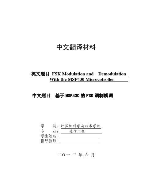
- 1、下载文档前请自行甄别文档内容的完整性,平台不提供额外的编辑、内容补充、找答案等附加服务。
- 2、"仅部分预览"的文档,不可在线预览部分如存在完整性等问题,可反馈申请退款(可完整预览的文档不适用该条件!)。
- 3、如文档侵犯您的权益,请联系客服反馈,我们会尽快为您处理(人工客服工作时间:9:00-18:30)。
第28卷 第2期吉首大学学报(自然科学版)Vol.28 No.2 2007年3月J ournal of J ishou University (Natural Science Edi ti on)Mar.2007 Article ID :1007-2985(2007)02-0059-04Design of RFID Reader Based on MCUMS P 430GE NG Shu qin,HOU Li gang,GUO Yue,W ANG Xiu ling,W U Wu chen(VLSI and System Lab,Beijing Universi ty of Technology,Beijing 100022,China)Abstract :Saving power is an important problem in portable device.This paper presents a SOC (System on a Chip)sys tem for radio frequency identification (RFID)reader to simplify the complex traditional circuits.It puts the peripheral circuits into SOCand uses software to e xec ute the decoding,checking,identifying and real time calculating and display ing of digital signals.The proposed system has advantages such as simple structure,low cost,and low power consump tion.Key words :RFID;reader;lo w power consumptionCLC number :TN47 Document code :B1 IntroductionRFID is one of automatic technology to identify and collect objec t data quickly through RF digital signals.RFID increases productivity and convenience.RFID is used for hundreds,if not thousands,of applications such as preventing theft of automobiles and merchandise,gaining entrance to buildings,automating parking [1],and so on.The thoughts of RFID occurred on the heels of the development of radar.An early,if not the first,work exploring RFID is the landmark paper by Harry Stockman, Communication by Means of Reflected Power published in 1948[2].RFID has advantages over bar code [3]:RFID does not require line of sight access to read the tag;the read range ofRFID is larger than that of a bar c ode reader;readers can simultaneously communicate with multiple RFID tags;be cause of this capability,a RFID reader can capture the contents of an entire shipment as it is loaded into a warehouse or shipping c ontainer;a reader collects detail information in one pass,without having to scan each product;tags can store more data than bar c odes.F ig .1 Block D iagram of a General Passive RFID System In general,RFID system comprises a reader (or interrogator),its associa ted antenna and the transponder (ortag)that carries data (see fig.1).Depending on theirsource of electrical power,there are active and passive twogeneral categories.Active RFI D ta gs contain an on boardbattery.Passive ta gs obtain po wer from the signal of reader.This paper deals with the passive ta g reader of 125kHz.The reader is usually controlled by micro controller of MC S51or arm.The former has high voltage,and much pow Received date :2007-01-20Foundation item :T he National Reform Commi ttee of Development Next Internet Demonstrative Subproject (CNGI-04-10-1D)Biography :GENG Shu qin(1970-),female,was born in Yuncheng City,Shaanxi Province,a doctor s tudent in Beijing University of Technology;the major research areas are the field of system integration,sensor and RFID.er c onsumption,with many peripheral circuits in the control system of RFID reader.It is not convenient to adjust the system and the area of PCB is big.The latter has high price,and the c ontrol system is complex.This paper presents a RFID reader system based on MSP430,which puts much peripheral circuits into a chip.It uses software to e xecute the decoding,checking,identifying and real time calculating and displaying of digital signals.The proposed syste m has ad vantages such as simple structure,low cost,and low power consumption.2 Functions of System2.1The Passive Tag ReaderThe reader is composed of RF. Module and micro controller (see fig.1).The reader transmits a low power radio signal through its antenna of RF. Module.When a tag c omes within the reader !s range,it receives an electromagnetic signal from the reader through the tag !s antenna.The tag then stores the energy from the signal,a process called inductive coupling [3].When the tag has built up enough charge,it can po wer a back end integrated circuit (chip)of the tag,which transmits a modulated signal to the reader.That return signal contains the information stored in the tag.Once the RF. Module received the data it can be sent to a micro c ontroller (or computer)for processing and management.At the same time,the processed data will be sent to LCD for display.2.2Communication Between Reader and TagBiot Savart la ws establish the relationship between the current I 1flowing in an electrical circuit having length l and the intensity of the magnetic induction B as function of the distance x be tween the measurement P point (of unit vector z ,shown in fig.2)and the element dl producing the field according to the formula [4]:d B = 0(I 1∀d l )#e z 4 x 2.Fig .2 Magnetic Field Strength F ig .3 Electric Equivalent Circuits for Magnetic(the Axis of the Coil )Coupling of Reader and Tag z is the axis of the coil.The total intensity of the magnetic induction of reader antenna is:B z (d ,r )= 0N 1I 1r 22(r 2+d 2)3/2.The electric equivalent circuit for Magnetic Coupling of Reader and tag is depicted in fig.3.As the previous sec tion has shown,this system works on the principle of Magnetic Coupling.The reader antenna resonant circuit is con structed by a capacitor C 1with an inductance L 1and the resistance R 1.The circuit of tag antenna is simplified as L 2,R 2,with the capacitance C 2,and the data load R L[4].Where para meter I shows the current of antenna;U 1is the source of ac signal voltage;U 2is the load voltage.The subscript 1indicates the side of reader;the subscript 2denotes the side of tag.The voltage of reader antenna is U 1= L 1I 1= !1.When tag enters the field of reader,such as P point,the flux that goes through tag antenna is !2=B Z S 2N 2.Acc ording to Faraday !s Law,if !2(t )=B Z S 2N 2=!2sin( t ),then u 20(t )=-d !2(t )/d t = !2cos( t ).Value of the coupling coefficient is M =k L 1L 2.The relation of signal volt 60吉首大学学报(自然科学版)第28卷age between reader and tag antenna is:U 20/U 1=k L 2/L 1.3 S ystem Architecture3.1Reader SystemFig .4 Reader System Frame of MSP 430F 435Reader syste m frame is consisted of RF. Module,LCD,keys,MC UMSP430and power.Reader system fra meof MSP430is shown as in fig. 4.This syste m uses lowpower consumption MC UMSP430that is a system on chipas the controller.The voltage is at 1.8~3.6V.3V ischosen by this system.The MSP430ultra lo w po wer architecture e xtends battery life.Current of RAM retention is0.1 A;a real time clock mode current is 0.8 A;currentof active state is 250 A 1MlPS.The clock system is de signed specifically for battery po wered applications.A lo w frequency auxiliary clock (ACLK)is driven directly from a common 32kHz watch crystal.The ACLK can be used for a background real time clock self wake up function.This low frequency auxiliary clock makes stand by mode ultra low power.An integrated high speed digitally controlled oscil lator (DCO)can source the master cloc k (MCLK)used by the CP U and high speed peripherals.By design,the DC O is active and stable in less than 6 s.This high speed master clock achieves high performance signal processing.MSP430 based solutions effectively use the high performance 16 bit RISC C PU in very short bursts.MSP430has LCD controller,which can directly drive LCD displays.It simplifies the complex circuits of traditional electrical LCD display system and solves the additional error problems.It puts the peripheral circuits into SOC.This can reduce the area and power consumption of PCB and minify the portable RFID system.Fig.3shows RF. Module c ommunicating with MCUMSP430.It can be seen that LC D module is linked with MSP430by I O in fig. 3.LCD gets data from I O of MC UMSP430and then displays them.W hen there is ta g in the reader radio field,RF. Module will receive signals.At the same time,the interrupt will wake up CP U in less than 6 s.Then CPU processes da ta and LCD displays them.When CPU has operated the interrupt,it will be set in the ultra low power stand by mode by the software.If there is not tag for a long time,LCD display is set to low po wer state.There are 20keys in this system,which are linked with CPU.RF. Module and Ke ys are connected with the interrupt pins.If there is no interrupt signals,system are in lo w power state.The soft frame is shownin fig.5and fig.6.Fig .5 Reader System Software Frame Fig .6 Identification Subprogram of Interruption3.2Communication Between RF . Module and MC UThe communication between RF. Module and MC U is as in fig.7:There is one byte as the start data and one 61第2期 耿淑琴,等:基于MSP430控制的射频识别读写器设计byte as the end data.The middle part is the ciphered data and longitudinal redundancy check (LRC)[5]data.RF.Module data and LRC data are sent together to the MC U.When their XOR result is zero,the data is right.Then data are sent to LC D for display,decoding and processing them.For example,one ta g I D number is 51E2066CED.Their ci phered c odes are 35H,31H,45H,32H,30H,36H,36H,43H,45H,and 44H.Longitudinal redundancy checksum is (51H)XOR (E2H)XOR (06H)XOR (6C H)XOR (EDH),and the checksum equals 34H.Together with the start bit 01,ciphered data,checksum and stop bit 02,the total number is 01353145323036364345443402.If MCU MSP430gets the data,it must take out the ciphered data with the checksum data,and execute the longitudinal redun dancy check.If the checksum of MC U is zero,it will decode the ciphered da ta.Identifying,real time calculating and displaying of digital signals must be carried out.If the checksum of MCU is not zero,this means that there are some er rors in the data.Then MCUMSP430will ask the RF. Module to send the data again.start bit Ciphered data Checksum stop bitFig .7 Data F orm Between RF . M odule and MC UFig .8 Data TimingIf MC U wants to get data correctly,it must applywith the data timing as fig.8.Clock frequency must beset seriously,and the time of instruc tors must be calculated correctly.Or else,experiment data may be wrong.Itwill take a lot of time to adjust and do experiments.4 ExperimentsTable 1sho ws power consumption of CP U and system at different state.W hen CPU is at stand by state,current is the ac tive state !s 39.2%.Power c onsumption of the stand by state can be reduced to 61%of the active state.Table 1 CPU Power Consumption of 125kHz RFID SystemCPU StateCPU I m A Power Consumption mW Active0.0280.61600Stand by LP30.0110.02420Sleeping 0.0100.000225 SummaryThis paper presents a RFID reader system for 125kHz to simplify the complex circuits of traditional system and to solve the additional error problems.It puts the peripheral circuits into SOC and uses software to execute the dec oding,checking,identifying and real time calculating and displaying of digital signals.The proposed system has advantages such as simple structure,low cost,and low power consumption.This system is successfully used in 125kHz RFID.References :[1] LANDT J.POTENTIALS.IEEE.History of RFID [J].Potentials,IEEE,2005,24(4):8-11.[2] HARRY municati on by Means of Reflected Power [J].Proceeding of the I.R.E,1948,36:1196-1204.[3] RAO K V S.An Overview of Backscattered Radio Frequency Iden tification System (RFID)[J].IEEE Microwave Conference,AsiaPaci fic,1999,3:746-749.[4] DOMINIQUE PARET.Translated by Roderick Riesco,RFID and Con tactless Smart Card Applications [M].England:John Wiley &Sons Ltd.,2005.[5] CORR P.A Statistical Evaluation of Error Detection Cyclic Codes for Data Transmissi on [J].Transactions on Communications Systems,1964,49:211-216.(下转第74页)Teleportation of Two Partite Arbitrary States Via GenuineFour Partite Entangled StatesKONG Yong hong,W ANG Xin wen(Department of Electronic Engineering and Physics,Hunan Uni versity of Science and Engineering,Yon gzhou425100,Hunan China)Abstract:A scheme for teleportation of two partite arbitrary states via genuine four partite entangled states is proposed. In the sche me,16orthogonal and complete bases are constructed.All the bases are genuine four partite entangled states,none of which is reducible.The scheme reveals some particular properties of the rela ted four partite entangled state,and indicates that in some sense the amount of entanglement of two Bell states can be abstracted from any one of the four partite states.Key words:four partite entangled states;two partite arbitrary states;orthogonal and complete bases;teleportation(责任编辑 陈炳权) (上接第62页)基于MSP430控制的射频识别读写器设计耿淑琴,侯立刚,郭 跃,王秀玲,吴武臣(北京工业大学集成电路与系统实验室,北京 100022)摘 要:设计了一种基于单片机处理器的射频识别(RFID)便携式读写器的系统.采用当前先进的片上系统(System on Chip,SOC),将外围电路尽可能地放置于SOC芯片内,利用软件实现了对射频标签信号的数字实时采集和控制功能,从而简化了传统的微控制器控制的RFID读写器所需的庞大硬件电路及其引入的额外误差,具有重要的实用价值,并且功耗和成本很低.关键词:射频识别;读写器;低功耗中图分类号:TN47文献标识码:B(责任编辑 陈炳权)。