KPF010D01中文资料
北京正北元电器有限公司

10,16,20A
33
6A
30
72
105
142
37
88
124
177
80A
83
187
250
376
25,32A
37
10A.16A.20A
22
53
86
113
30
72
110
161
100A
92
209
282
417
BM65NL-32相线+中性漏电断路器
25A.32A
24
59
93
123
35
82
120
166
125A
1500
BM30-225/4300A
1000
BM30L-225/3300
1400
BM30-225L/3300
600
BM30-800M/3300
1650
BM30-225/4300B
1050
BM30L100/4300A,B
1200
BM30-225M/3300
800
BM30-800H/3300
2150
BM30-400/4300A
131000
BW1-3200/3200 3P固定式
28500
BW1-6300/4000 3P抽出式
73000
BW1-2000/630 4P抽出式
17500
BW1-4000/3600 3P固定式
41500
BW1-6300/5000 3P抽出式
81000
BW1-2000/800 4P抽出式
19000
BW1-4000/4000 3P固定式
REF01中文手册

REF01数据表1、元器件参数特性1)High output accuracy(高输出精度)REF01: 10.0 V, ±0.3% maximumREF02: 5.0 V, ±0.3% maximumREF03: 2.5 V, ±0.6% maximum2)Excellent temperature stability(良好的温度稳定特性)REF01: 8.5 ppm/°C maximumREF02: 8.5 ppm/°C maximumREF03: 50 ppm/°C maximum3)Low noise(低噪声)REF01: 30 µV p-p typicalREF02: 15 µV p-p typicalREF03: 6 µV p-p typical最高供电电压范围:最大达36 V最低供电电流:最大值为1.4 mA高负荷驱动能力:最大10 mA(最大输出负载电流)温度输出功能(温度监控)应用场景精密数据系统高分辨率转换器工业过程控制系统精密仪器军事和航空航天应用概述REF01/REF02/REF03系列精密电压参考产品提供了稳定的10.0 V、5.0 V或2.5 V输出,且随供应电压、环境温度或负载条件的变化影响最小。
该设备有8引脚的SOIC、PDIP、CERDIP 和TO-99封装,以及20端口的LCC封装(仅883),进一步提高了该设备在标准和高压力应用中的可用性。
通过一个外部缓冲器和一个简单的电阻网络,TEMP终端可以用于温度传感和近似。
在该装置上还提供了一个TRIM端子,用于微调输出电压。
REF01、REF02/REF03系列应用非常适合通用和空间受限的应用。
较新的设计应使用ADR01/ADR02/ADR03/ADR06系列参考文献,可提供更高的精度和温度。
1、引脚配置不同封装下的引脚图如下:注:NC = NO CONNECT ,即不要在这些引脚上连接任何东西。
KPF070D01中文资料

FEATURESLow pressure (0~1)Easy to use dual in-line package (DIP)Wide 0~60compensated temperature range Span calibration to 2% for low pressure Zero offset calibrationHigh performance, stable packaged silicon chip Gage and differential pressure configurationsAPPLICATIONSMedical Equipment Respiration HVACLevel Detection Flow Measurement Industrial ControlMODEL NUMBER FOR ORDERINGMAXIMUM RATINGOperating Input Current 1.5constant, Ambient Temperature Ta=25mV 2mV 2.50.650.32.02.0PIN CONFIGURATIONRELIABILITY TESTCover 9.40 13.973.3 OD 2.03ID PACKAGE CONFIGURATION AND DIMENSIONS (U nit : mm )120, 1000hrs-40, 1000hrs255, 1 million times, Rated Pressure -20, 1 million times, Rated Pressure100, 1 million times, Rated Pressure 40, 90%RH, 1 million times, Rated Voltage 260, 10 seconds -40~120, 30minutes/1Cycle, 100Cycles Amplitude : 1.5mm, Frequency : 10~55Hz,X, Y, Z(3-directions), 2 hrs each direction 75cm height, 2 timesBending Strength : 4.9N(0.5kgf), Right/Left 90, 1time 230, 5 secondsNote1. Mounting on printed circuit boardsWhen mounting a transistor on a printed circuit, it is assumed that lead wires will be processed or reformed due to space limitation or relations with other components. Even if no such special processing reforming is conducted exercise care on the following points :(a) Make the spaces of lead wire inserting holes on the printed circuit board the same as those of lead wires on a transistor.(b) Even if The spaces are not the same, do not pull the lead wires or push heavily against the sensor element.(c) Use a spacer for form a lead maintain space between a sensor and a printed circuit board, rather than closely contacting them with each other.(d) When forming a lead prior to mounting onto a board- Bend the lead at a point 3mm or more apart from the body(Lead root).- Bend one lead wire after securing the other lead wire. (near the main body)- Keep space between the sensor main body and and a fixing jig.- When bending the lead along the jig, be careful not to damage it with an edge of the jig.- Follow other precautions described in respective standard (e) When mounting a sensor onto a heat sink - Use the specified accessory.- Drill threaded holes on the heat kink as per specifications and keep the surface free from burrs and undulations.- Use KEC’s recommended silicon grease.- Tighten the screw within the specified torque.- Never apply a pneumatic screwdriver to a transistor main body.(f) Do not bend or stretch the lead wires repeatedly.When pulling in the axial directions, apply 500g or 600gpower, depending on the shapes of lead wires.2. SolderingWhen soldering a sensor to a printed circuit board, the soldering temperature is usually so high that it adversely affects the sensor.Normally, tests are conducted at a soldering temperature of 265for 10 seconds or 300for 3 seconds. Be sure to complete soldering procedures under these conditions of temperature and time.Be careful to select a type of flux that will neither corrode the lead wires nor affect the electrical characteristics of a sensor.The basic precautions for soldering procedures are as follows :(a) Complete soldering procedures in a time as short as possible.(b) Do not apply stress to a sensor after soldering by correcting or modifying its location or direction.(c) For a sensor employing a heat sink, mount it on the heat sink first: then solder this unit to a printed circuit board after confirming that it is fully secured.(d) Do not directly solder the heat-radiating portion of a sensor to a printed circuit board.(e) In flow solder jobs, sensors are apt to float on the solder due to solder surface tension. When adjusting the locations of sensor, be careful not to apply excessive stress to the roots ofthe sensor lead wires.(f) When using a soldering iron select those which have less leakage, and be sure to ground the soldering iron.3. Cleaning a circuit boardAfter soldering, circuit boards must be cleaned to remove flux.Observe the following precautions while cleaning them(a) When cleaning circuit boards to remove flux, make sure that no residual reactive ions such as Na or Cl ions remain. Note that organic solvents react with water to generate hydrogen chloride and other corrosive gases which can degrade device performance.(b) Do not rub the indication marks with a brush or one ’s fingers when cleaning or while a cleaning agent is applied to the markings.(c) There are ultrasonic wave cleaning methods which offer a high cleaning effect within a short time. Since there methods involve a complicated combination of factors such as the cleaning bath size, ultrasonic wave vibrator output, andprinted circuit board mounting method, there is fear that theservice life of airtight seal-type sensors may be extremely shortened. Therefore, as far as possible avoid using the ultrasonic wave cleaning method.- Basic requirements of ultrasonic wave cleaning method.Frequency : 27~29kHzOutput : 300W or less (300W/or less)Recommended solvents : Refer to details above Cleaning time : 30seconds or less。
F 系列产品说明书

F系列产品使用说明书安装操作手册注意事项:!请勿将重物至于本设备上;!请勿让任何固体或液体,掉入或渗入设备内;!请定期用刷子对电路板、接插件、机箱风机、机箱等进行除尘,在进行机体清洁工作前,请关闭电源并拔掉电源;!请勿自行对本设备进行拆卸、维修或更换零件;!避免强烈的碰撞,请勿摔落机器;!仅可在额定输入输出范围内使用。
使用环境:!请在0℃~40℃的温度下放置和使用本产品,避免阳光直射,或靠近热源;!请勿将本设备安装在潮湿的环境;!请勿将本设备暴露在多烟、多尘的环境;!请保持本产品的水平安装,安装在稳定的场所,注意防止本产品坠落;!请安装在通风良好的场所,切勿堵塞本产品的通风口。
目录第一章产品介绍 (5)1.1 产品概述 (5)1.2 产品主要功能 (5)第二章开箱检查和线缆连接 (7)2.1 开箱检查 (7)2.2 硬盘安装 (7)2.3 在机架中安装 (8)2.4 前面板 (8)2.5 后面板 (10)2.6 安装连接示意图 (10)2.7 音视频输入输出连接 (11)2.7.1 视频输入的连接 (11)2.7.2 视频输出设备的选择和连接 (11)2.7.3 音频信号的输入 (11)2.7.4 音频输出 (12)2.8 报警输入输出连接 (12)2.8.1 报警输入端口说明 (13)2.8.2 报警输出端口说明 (14)2.8.3 报警输出端继电器参数 (14)2.9 球机连接 (14)第三章基本操作 (16)3.1 开机 (16)3.2 关机 (16)3.3 登录 (16)3.4 预览 (17)3.5 桌面快捷菜单 (17)3.5.1 主菜单 (18)3.5.2 录像控制 (18)3.5.3 录像回放 (19)3.5.4 云台控制 (21)3.5.5 报警输出 (25)3.5.6 图像颜色 (26)3.5.7 输出调节 (26)3.5.8 关闭系统 (27)3.5.9 页面切换 (27)第四章主菜单 (28)4.1 主菜单导航 (28)4.2 录像功能 (29)4.2.1 录像设置 (29)4.2.2录像回放 (31)4.2.3 图片存储 (31)4.2.4 录像备份 (32)4.3 报警功能 (33)4.3.1 移动侦测 (33)4.3.2 视频遮挡 (35)4.3.3 视频丢失 (36)4.3.4 报警输入 (36)4.3.5 报警输出 (37)4.3.6 异常处理 (37)4.4 系统设置 (37)4.4.1 普通设置 (38)4.4.2 编码设置 (39)4.4.3 网络设置 (40)4.4.4 网络服务 (41)4.4.5 输出模式 (49)4.4.6 云台设置 (50)4.4.7 串口设置 (50)4.4.8 轮巡设置 (51)4.5 管理工具 (51)4.5.1 硬盘管理 (51)4.5.2 用户管理 (52)4.5.3 在线用户 (55)4.5.4 输出调节 (55)4.5.5 自动维护 (55)4.5.6 恢复默认 (56)4.5.7 系统升级 (56)4.5.8 设备信息 (57)4.6 系统信息 (57)4.6.1 硬盘信息 (57)4.6.2 码流统计 (58)4.6.3 日志信息 (59)4.6.4 版本信息 (59)4.7 关闭系统 (60)第五章常见问题解答及使用维护 (61)5.1 常见问题解答 (61)5.2 使用维护 (66)附录1.遥控器操作 (67)附录2.鼠标操作 (68)附录3.硬盘的容量计算 (69)附录4.技术参数 (70)第一章产品介绍1.1 产品概述本设备是专为安防领域设计的一款优秀的数字监控产品。
Parker Hannifin 电子比例阀CANopen接口型号D1FB和D3FB的技术文档说明书

D3FB*C*0Spool/Sleeve DesignD3FB*CD*FB*KD*FB*E D*FB*CGeneral DescriptionSeries D1FB (NG6) and D3FB (NG10) proportional directional valves with CANopen interface are based on the series for standard digital electronics of the same name.CANopen-ProfileCANopen Application Layer and Communication Layer CiA DS - 301 Version 4.01CANopen Layer Setting Services (LSS) and Protocols CiA DS – 305 Version 2.0Device Profile in accordance with CiA DSP – 408 Version 1.5.2The baud rate and node ID can be set by dip switches or Layer Setting Service (LSS).The valve parameters are factory set. Additionally the ProPxD software permits the editing of all parameters via the separate communication port. The software is also used for the valves with digital onboard electronics and the electronics modules. The cable for connection to a serial RS232 interface is available as accessory.The digital onboard electronics is situated in a robust metal housing and can be used in rough environments.The series D1FB and D3FB are available with spool/sleeve design as well as with spool/body design.Features• CANopen interface.• Spool/sleeve design and spool/body design.• High repeatability from valve to valve.• Low hysteresis.• Manual override.• Failsafe center position.Directional ControlSizeFlowStyleSealOptions Weight:D1FB2.5 kg (5.5 lbs.)Spool DesignCode DescriptionSpool/sleeve design3Spool/body designDesign Series NOTE: Not required when ordering.Standard Bolt Kit:BK209 (4) 10-24x1.25 SHCS BK375 4x M5x30Parametrizing cable OBE => RS232 Item no. 40982923CommunicationDesign Series NOTE: Not required when ordering.Directional ControlSizeFlow StyleSealWeight:D3FB7.0 kg (15.4 lbs.)Parametrizing cable OBE => RS232 Item no. 40982923Spool OptionsDesignCode DescriptionSpool/sleeve design3Spool/body designStandard Bolt Kit:BK98 (4) 1/4-20x1.625 SHCS BK385 4x M6x40Communication* Flow rate for different ∆p per control edge: Qx = QNom.· √ ∆p x∆p Nom.Continued on the next pageAll performance curves measured with HLP46 at 50°C (122°F).Flow LimitAt 25%, 50%, 75% and 100% command signal (symmetric flow). At asymmetric flow a reduced flow limit has to be considered – typically approx. 10% lower.All performance curves measured with HLP46 at 50°C (122°F).Flow LimitAt 25%, 50%, 75% and 100% command signal (symmetric flow). At asymmetric flow a reduced flow limit has to beconsidered – typically approx. 10% lower.All performance curves measured with HLP46 at 50°C (122°F).All performance curves measured with HLP46 at 50°C (122°F).Flow Limit100% command signal (symmetric flow). At asymmetric flow a reduced flow limit has to be considered – typically approx. 10% lower.All performance curves measured with HLP46 at 50°C (122°F).Series D*FB with CANopenSupply Voltage Connection 6 + PEA Supply voltage 18...30VB Supply voltage 0VC hCD hCE hCF hCG PECANopen ConnectionCAN in: M12, 5 pole male terminals. Pin 1: CAN_SHLD Pin 2: ncPin 3: CAN_GND Pin 4: CAN_H Pin 5: CAN_LShield is CAN_GND.CAN out: M12, 5 pole female terminals. Pin 1: CAN_SHLD Pin 2: ncPin 3: CAN_GND Pin 4: CAN_H Pin 5: CAN_L Shield is CAN_GND.Wiring ConnectionsSeries D*FB with CANopen Technical InformationNode–ID Adjustment with DIP SwitchesBaud Rate Adjustment with DIP SwitchesSeries D*FB with CANopenTechnical Information The parametrizing cable may be ordered under item no. 40982923.Features• Simple editing of all parameters.• Storage and loading of optimized parameter adjustments.• Executable with all Windows ®operating systems fromWindows ® 95 upwards.• Communication between PC and electronics via serial interface RS-232.• Simple to use PC user software, free of charge:/euro_hcd – see "Software Downloads"ProPxD Interface ProgramThe ProPxD software permits comfortable param-eter setting for the module electronics. Via the clearly arranged entry mask the parameters can be noticed and modified. Storage of complete parameter sets is possible as well as printout or record as a text file for further documentation. Stored parameter sets may be loaded anytime and transmitted to other valves. Inside the electronics a nonvolatile memory stores the data with the option for recalling or modification.D1FB*CD1FB*ED3FB*C OBED3FB*E OBE。
SMD0805P010TF中文资料

Dimensions (mm) Model
SMD0805P010TS/TF SMD0805P020TS/TF SMD0805P035TS/TF SMD0805P050TS/TF SMD0805P075TS/TF SMD0805P100TS/TF
1.0
1.0
A
B
C
D
E
packaging quantity
WebLinks
Further info see:
Further application info see fuseology: /download/fuseology.pdf
Solder pad Layout (mm)
040617 E-mail: sales@ E-mail: service@ E-mail: sales@ E-mail: sales@
元器件交易网
1.50 @ 0.50 0.02 @ 8.00 0.10 @ 8.00 0.10 @ 8.00 0.20 @ 8.00 0.30 @ 8.00
0.5
1.000
3.500
6.000
••
0.5
0.650
2.000
3.500
••
Hale Waihona Puke 0.50.2500.750
1.200
••
0.5
0.150
0.500
0.850
••
Hold current: maximum current device will pass without tripping in 20 °C still air. Trip current: minimum current at which the device will trip in 20 °C still air. Maximum voltage device can withstand without damage at rated current (I max) Maximum fault current device can withstand without damage at rated voltage (Vmax)
欧诺克 直流无刷电机 产品说明书

深圳市欧诺克科技有限公司Shenzhen ONKE Technology Co., Ltd.座机:*************27381841电话:邓先生135****7106陈先生139****0920邮箱:***************网 址 : 地址:广东省深圳市宝安区福海街道怀德翠湖工业园13栋稳定的质量是我们赖以生存的根本优质的服务是我们继续发展的前提客户的满意是我们唯一追求的目标产品画册Product gallery专业生产伺服驱动器、伺服电机及自动化控制系统深圳市欧诺克科技有限公司直流无刷电机目录匠心制造精益求精“一、公司介绍01二、直流无刷电机021.电机介绍与型号说明032.电机应用领域043.电机规格参数表054.电机规格尺寸图06C O M P A N Y PROFILE以精密制造引领未来Leading the future with precision manufacturing公司简介Company Profile深圳市欧诺克科技有限公司成立于2010年,是一家专业研发生产伺服电机和驱动器的高新技术企业,公司技术力量雄厚,检测手段先进,欧诺克人本着不求最全,只求最精的信念,为生产出各类伺服电机、各类驱动器而不懈奋斗。
欧诺克人以鹰的精神,挑战尖端,研发生产出高性价比的各类伺服电机和驱动器,以鹰的敏锐洞察力洞察市场,与时俱进、创新来满足市场的需求。
深圳市欧诺克科技有限公司产品主要有:伺服驱动器、伺服电机、直流伺服驱动器,直流伺服电机,交流伺服驱动器,交流伺服电机,低压伺服驱动器,低压伺服电机,直线电机驱动器,DDR马达驱动器,音圈电机驱动器,直流无刷驱动器,直流无刷电机,CANopen总线、EtherCAT总线、电子凸轮伺服系统,大功率伺服驱动器、大电流伺服驱动器,专用运动控制伺服驱动器和自动化控制系统,十多年来凭借精湛的技术与国内国外众多知名企业公司建立了互利共赢的合作。
公司不断研究和开发满足行业需求的各类伺服电机和驱动器,帮助客户提升品质和生产效率。
D1D07资料
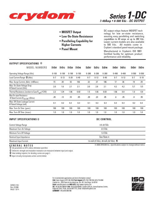
Series 1-DC
7-40Amp • 0-500 Vdc - DC OUTPUT
• MOSFET Output • Low On-State Resistance • Paralleling Capability for
Higher Currents • Panel Mount
0.3 0.3 100 100 1.0 1.0
D5D07 D5D10
0-500 0-500 0-7 0-10
19
29
5.7 5.5
1.0 0.8
.8 .55
0.2 0.3 100 100 1.0 1.0
INPUT SPECIFICATIONS 1
Control Voltage Range Maximum Turn-On Voltage Minimum Turn-Off Voltage Nominal Input Impedance Maximum Input Current
INPUT
4 (–)
Input and output polarity must be observed. Inductive loads must be diode suppressed.
1 (–) LOAD
OUTPUT
SSR
(–)
(+)
3 (+)
2 (+)
MAX. SURGE CURRENT (Amps)
Screw Torque Requirements: 6-32 Screws - 10 in. lbs. (1.1Nm), 8-32 and 10-32 Screws - 20in. lbs. (2.2Nm) (Screws dry without grease.)
- 1、下载文档前请自行甄别文档内容的完整性,平台不提供额外的编辑、内容补充、找答案等附加服务。
- 2、"仅部分预览"的文档,不可在线预览部分如存在完整性等问题,可反馈申请退款(可完整预览的文档不适用该条件!)。
- 3、如文档侵犯您的权益,请联系客服反馈,我们会尽快为您处理(人工客服工作时间:9:00-18:30)。
FEATURESLow pressure (0~1)Easy to use dual in-line package (DIP)Wide 0~60compensated temperature range Span calibration to 2% for low pressure Zero offset calibrationHigh performance, stable packaged silicon chip Gage and differential pressure configurationsAPPLICATIONSMedical Equipment Respiration HVACLevel Detection Flow Measurement Industrial ControlMODEL NUMBER FOR ORDERINGMAXIMUM RATINGOperating Input Current 1.5constant, Ambient Temperature Ta=25mV 2mV 2.50.650.32.02.0PIN CONFIGURATIONRELIABILITY TESTCover 9.40 13.973.3 OD 2.03ID PACKAGE CONFIGURATION AND DIMENSIONS (U nit : mm )120, 1000hrs-40, 1000hrs255, 1 million times, Rated Pressure -20, 1 million times, Rated Pressure100, 1 million times, Rated Pressure 40, 90%RH, 1 million times, Rated Voltage 260, 10 seconds -40~120, 30minutes/1Cycle, 100Cycles Amplitude : 1.5mm, Frequency : 10~55Hz,X, Y, Z(3-directions), 2 hrs each direction 75cm height, 2 timesBending Strength : 4.9N(0.5kgf), Right/Left 90, 1time 230, 5 secondsNote1. Mounting on printed circuit boardsWhen mounting a transistor on a printed circuit, it is assumed that lead wires will be processed or reformed due to space limitation or relations with other components. Even if no such special processing reforming is conducted exercise care on the following points :(a) Make the spaces of lead wire inserting holes on the printed circuit board the same as those of lead wires on a transistor.(b) Even if The spaces are not the same, do not pull the lead wires or push heavily against the sensor element.(c) Use a spacer for form a lead maintain space between a sensor and a printed circuit board, rather than closely contacting them with each other.(d) When forming a lead prior to mounting onto a board- Bend the lead at a point 3mm or more apart from the body(Lead root).- Bend one lead wire after securing the other lead wire. (near the main body)- Keep space between the sensor main body and and a fixing jig.- When bending the lead along the jig, be careful not to damage it with an edge of the jig.- Follow other precautions described in respective standard (e) When mounting a sensor onto a heat sink - Use the specified accessory.- Drill threaded holes on the heat kink as per specifications and keep the surface free from burrs and undulations.- Use KEC’s recommended silicon grease.- Tighten the screw within the specified torque.- Never apply a pneumatic screwdriver to a transistor main body.(f) Do not bend or stretch the lead wires repeatedly.When pulling in the axial directions, apply 500g or 600gpower, depending on the shapes of lead wires.2. SolderingWhen soldering a sensor to a printed circuit board, the soldering temperature is usually so high that it adversely affects the sensor.Normally, tests are conducted at a soldering temperature of 265for 10 seconds or 300for 3 seconds. Be sure to complete soldering procedures under these conditions of temperature and time.Be careful to select a type of flux that will neither corrode the lead wires nor affect the electrical characteristics of a sensor.The basic precautions for soldering procedures are as follows :(a) Complete soldering procedures in a time as short as possible.(b) Do not apply stress to a sensor after soldering by correcting or modifying its location or direction.(c) For a sensor employing a heat sink, mount it on the heat sink first: then solder this unit to a printed circuit board after confirming that it is fully secured.(d) Do not directly solder the heat-radiating portion of a sensor to a printed circuit board.(e) In flow solder jobs, sensors are apt to float on the solder due to solder surface tension. When adjusting the locations of sensor, be careful not to apply excessive stress to the roots ofthe sensor lead wires.(f) When using a soldering iron select those which have less leakage, and be sure to ground the soldering iron.3. Cleaning a circuit boardAfter soldering, circuit boards must be cleaned to remove flux.Observe the following precautions while cleaning them(a) When cleaning circuit boards to remove flux, make sure that no residual reactive ions such as Na or Cl ions remain. Note that organic solvents react with water to generate hydrogen chloride and other corrosive gases which can degrade device performance.(b) Do not rub the indication marks with a brush or one ’s fingers when cleaning or while a cleaning agent is applied to the markings.(c) There are ultrasonic wave cleaning methods which offer a high cleaning effect within a short time. Since there methods involve a complicated combination of factors such as the cleaning bath size, ultrasonic wave vibrator output, andprinted circuit board mounting method, there is fear that theservice life of airtight seal-type sensors may be extremely shortened. Therefore, as far as possible avoid using the ultrasonic wave cleaning method.- Basic requirements of ultrasonic wave cleaning method.Frequency : 27~29kHzOutput : 300W or less (300W/or less)Recommended solvents : Refer to details above Cleaning time : 30seconds or less。