激光加工形成硅基上的氧化低维纳米结构的PL发光
光电功能化的低维材料与器件研究

光电功能化的低维材料与器件研究光电功能化低维材料已成为当前材料科学研究和应用开发的热点领域之一。
低维材料是一类在一个或两个维度上尺寸极小的材料,具有独特的物理和化学特性。
与传统三维材料相比,低维材料的电子、光学、热学和力学性能更加优越,具有更宽的光谱响应范围和更高的效率。
光电功能化的低维材料和器件研究已成为国内外研究的热点和难点,其研究成果也已广泛应用于光电信息存储、光电控制、能源转换和生物医学等领域。
一、低维材料的分类与特性低维材料是在一个或两个维度上尺寸极小的材料,主要包括一维纳米线、二维薄膜和量子点等。
这些材料的特性包括:1. 电子性能:低维材料具有载流子与晶格耦合减弱、表面自由能增大、接触电势变化明显等电子性能特征。
这些特征促进了低维材料在太阳能电池、光电控制器等光电器件上的应用。
2. 光学性能:低维材料具有更宽的光响应范围、更高的量子效率和更小的逸出功。
这些特性对实现高效发光器件、太阳能电池、光电传感器等光电器件具有重要意义。
3. 热学性能:低维材料有更小的热容量和更大的界面效应,可用于制造热电转换器件,实现能源和热能的高效转换。
4. 力学性能:低维材料在弯曲和拉伸等情况下,会出现四面体效应和屈曲现象,其力学性能表现更为复杂。
这些特性在制造柔性电子设备和高强度材料等领域有重要应用。
二、光电功能化低维材料的制备低维材料的制备包括物理法、化学法和生物法等多种方式。
其中物理法包括真空蒸发、物理气相沉积和激光热解法等;化学法包括溶液法、气相沉积法和水热法等;生物法则是利用生物体系中的生物分子来制造低维材料或通过仿生学方法来合成低维材料。
近年来,通过表面修饰等手段,光电功能化低维材料多样性不断增强,使得低维材料的应用范围更为广泛。
例如,将金属氧化物、过渡金属硫化物、碳纳米管等多种材料与量子点、纳米线和薄膜等低维材料相结合,可以获得具有特殊性质和高效性能的光电功能化材料。
三、光电功能化低维材料的应用光电功能化低维材料在光电器件、能源转换和生物医学等领域的应用广泛。
硅基上低维结构的受激发光
摘
要 : 54 m 激 光抽 运 纳晶硅 样品 时 , 用 1n 我们 观 测到表 面上氧 化 结 构在 62 m 和 64 m 处 的 9n 9n
尖锐 受激 发光 , 明显 的 闽值 行 为证 明 了它的 受激 辐射 特 性 。 纳 晶硅 氧 化 结 构通 过 激光 辐 照 和 其
Байду номын сангаас
退 火处理 来形 成 。解释 这种 受激 辐射 的模 型 已提 出, 中纳 晶硅 与氧 化 硅 之 间 的 陷 阱态起 着重 其
Z A G R n — o , N a-u ,Q N C a -a I h- n H N o gt WA G H i I h o i ,LU S i og a x jn r
( . e aoaoyo P o eet nTc nl yadA pi t n G i o nvri ,G i n 5 0 5 hn ; 1 K yLb r r f ht lc o ehoo n p lai , uz uU i sy uy g 0 2 ,C ia t o r g c o h e t a 5
互作 用是 主要 的。
在我们最近的工作 中, 硅基上 的受激发光来 自陷阱态 电子与空穴 的复合 ( 为无声子过程 ) 。我们用 54 m的激光束照射样 品时 , 64 m 和 62 m处出现两个尖锐的受激发光峰 , 1n 在 9n 9n 它们来 自硅基上的一些
fc t e xd fslc n a d p rusna o r sa ly a mp ra tr l a e bewe n o i e o i o n o o n cy tlp a n i o t n oe. i Ke wo d y r s:S i l td e s in,Ox d tu t e o i c n,Tr p Stts tmu a e miso i e sr cur fsl o i a ae
半导体制造技术期末题库参考答案
(1) 、杂质分布形式:在表面浓度 Cs 一定的情况下,扩散时间越长,杂质 主要特点: 扩散的就越深,扩到硅内的杂质数量也就越多。
x 2 Dterfc 1 (2)、结深: j
CB A Dt Cs
x2
Cs 4 Dt C ( x, t ) | x ,t e (3)、杂质浓度梯度: x Dt
4、写出菲克第一定律和第二定律的表达式,并解释其含义。
费克第一定律 C 杂质浓度 D 扩散系数(单位为 cm2/s) J 材料净流量(单位时间内流过单位面积的原子个数) 解释:如果在一个有限的基体中杂质浓度 C(x, t)存在梯度分布,则杂质 将会产生扩散运动,杂质的扩散流密度 J 正比于杂质浓度梯度 C/ x,比 例系数 D 定义为杂质在基体中的扩散系数。 1、杂质的扩散方向是使杂质浓度梯度变小。如果扩散时间足够长,则杂质分布 逐渐变得均匀。 2、当浓度梯度变小时,扩散减缓。 3、D 依赖于扩散温度、杂质的类型以及杂质浓度等。 菲克第二定律
可得
代入第一定律方程则得到第二方程。即杂质在材料
中沿某一方向浓度随时间变化率是由于扩散所引起的。
5、以 P2O5 为例,多晶硅中杂质扩散的方式及分布情况。
由于 P2O5 的晶粒较大,因此主要形成 B 类分
6.分别写出恒定表面源扩散和有限表面源扩散的边界条件、初始条件、 扩散杂质的分布函数,简述这两种扩散的特点
如果假设扩散系数 D 为常数,这种假设在低杂质浓度情况下是正确的,则得
解释: 菲克第二定律即为一维扩散方程 沿扩散方向,从 x 到 x+Δx,面积为Δs 的一个小体积元内的杂质数量随时间的 变化情况。设在小体积元Δv=ΔxΔs 内的杂质分布是均匀的。体积元内的杂质 浓 度 为 C(x, t) , 经 过 Δ t 时 间 , 该 体 积 元 内 杂 质 变 化 量 为 ,杂质在 x 处的扩散流密度分别为 J(x,t)则 在 Δ t 时 间 内 通 过 x 处 和 x+ Δ x 处 的 杂 质 流 量 差 为 ,假设体积元内的杂质不产生也不消失,
低维纳米功能材料

(2) 在磁学性质方面的应用 当代计算机硬盘系统的磁记录密度超过1.55Gb/cm2,在这 情况下,感应法读出磁头和普通坡莫合金磁电阻磁头的磁致 电阻效应为3%,已不能满足需要,而纳米多层膜系统的巨 磁电阻效应高达50%,可以用于信息存储的磁电阻读出磁头, 具有相当高的灵敏度和低噪音。目前巨磁电阻效应的读出磁 头可将磁盘的记录密度提高到1.71Gb/cm2。同时纳米巨磁 电阻材料的磁电阻与外磁场间存在近似线性的关系,所以也 可以用作新型的磁传感材料。高分子复合纳米材料对可见光 具有良好的透射率,对可见光的吸收系数比传统粗晶材料低 得多,而且对红外波段的吸收系数至少比传统粗晶材料低3 个数量级,磁性比FeBO3和FeF3透明体至少高1个数量级, 从而在光磁系统、光磁材料中有着广泛的应用。
1·化学沉淀法 化学沉淀法是在金属盐类的水溶液中,控制 适当的条件使沉淀剂与金属离子反应,产生 水合氧化物或难溶化合物,使溶质转化为沉 淀,然后经分离、干燥或热分解而得到纳米 颗粒。该法可分为直接沉淀法、均匀沉淀法、 共沉淀法和醇盐水解法。
2.溶胶一凝胶法 溶胶一凝胶法是指金属有机或无机化合物经 过溶液、溶胶、凝胶而固化,再经热处理而 成为氧化物或其他化合物的方法。该方法可 实现分子水平的化学控制和介观水平的几何 控制,从而得到性能剪裁目的。
分子束外延(MBE) 在众多制备方法中,原子层沉积是当前被广 泛使用的一种方法,它可以制备大面积,均 匀性很好的薄膜,并且拥有对成膜速度的良 好控制。但是,它也有一些缺点,例如为了 获得均匀性良好的薄膜,必须在Si衬底上保留 一薄层Si02,这一层Si02对等效氧化层厚度 的减小无疑是个障碍。由于前驱体的使用, 剩余杂质的污染也是一个 严重的问题,它不 仅会影响器件的稳定性,甚至影响到薄膜的 结构特征。
多孔硅激光英文
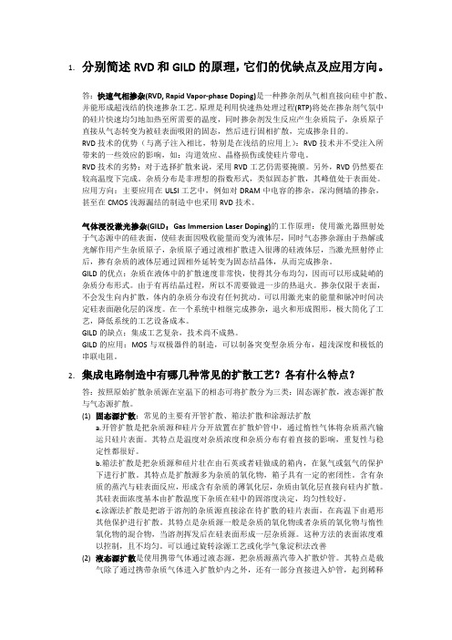
第26卷 第4期2008年12月 贵 州 科 学GU IZHO U SC IENC E Vol.26,No.4Dec.2008收稿日期资助项目国家自然科学基金资助项目(6)作者简介黄伟其,男,贵州大学,教授1多孔硅激光黄伟其,张荣涛,王海旭,金 锋(贵州光电子技术与应用重点实验室,贵州大学 贵州 贵阳 550025)摘 要 我们用波长为1064n m的纳秒脉冲激光在硅表面打出小孔结构,然后再做高温退火处理形成了硅的纳米氧化低维结构1在514nm激光泵浦下,发现该结构在700n m和750n m处有很强的受激辐射发光(P L)1实验中发现:该PL发光有明显的阈值表现和激光增强效应,证明该P L发光确实是光致受激发射1计算給出氧化界面态模型来解释该光致受激发光机理,其中Si=O和Si2O2S的键合可以产生氧化陷阱态,关键在于该氧化陷阱态与价带顶空穴态之间能够形成粒子数反转1为硅基上激光器件的光电子集成研发开辟了新的途经1关键词:光致荧光;多孔硅;陷阱态中图分类号 O472.3 文献标识码 A 文章编号 1003-6563(2008)04-0012-06L ASER O N PO RO US S IHUAN G W ei-qi,ZHANG Rong-tao,WAN G H a i-x u,J I N F eng(Key Lab.of Phot oelectron Technology and Appli ca ti on,Guizhou Uni ve rsity,Guiy ang550025)ABSTRAC T The p h otol um inescence(P L)of nanocrystal present in porous silicon s hifts fro m t he near infra2red t o t he ultraviol e t depend i ng on the size when the s urface is passivated with Si2H bonds.After oxidati on,thecenter wavelength of P L band is p i nned in the region of700n m~750nm and its intensity inc rease s obvi ously.Ca lcula ti on sho ws that trap electronic st a tes appea r in the band gap of t he s ma lle r nanoc rystal when Si=Obonds or Si2O2Si b onds are for m ed.The change s in PL intensity and wave l ength can be ex p l a ined by both quan2tum confine m ent and trap state s in oxida tion layer of nan ocrysta l.In the t heore tica l mode l,the most i m portantfac t or in the enhancem ent and p inning effec t of P L em ission is the relative position bet ween the l eve l of the trapstate s and the lev e l of the phot oexc itati on in the silicon nanoc rystal.KEY W O RD S phot olu m inescence;porous silicon;trap st a tes1 I ntroduc ti o nOf all the f or m s of silicon containing nanocrystal,por ous silicon is the one that ha s a ttrac ted the most attention to date[1,2],mostly because of its intense visible photolu m inescence(P L).N u m er ous models have been p r oposed to exp lain its PL.Presently,although a deta iled understanding of the P L ha s yet t o be achieved[2],it is usua lly accep ted that the band gap opens as a result of quantu m confine m ent,which pushe s the P L in the visible band for:2008-02-18:1074002:nanocrystal .P L of nanocrysta l present in por ous silicon can be turned fr om the nea r infrared t o the ultravi olet when the surf ace is passiva ted with Si 2H bonds .After oxida tion,the centerwavelength of P L band isp inned in the r egion of 700nm ~750nm.M.V .W olkin pr opose a model f or exp laining the p inning wavelength eff ect which is r e lated to the trapp ing of an electr on by Si =O bonds tha t p r oduce localized levels in the bandgap of s m aller nanocrystals[3].I n our calculation the Si 2O 2Si bonds or Si =O bonds on the surface of nanocrystal can all pr oduce the tr ap states .I nW olkin ’s model,it is indicated tha t the quantum confine m ent alone can exp lain the P L on por ous nano 2c r ystals lar ger than 3nm (displaying red or orange e m issi on),and the oxidati on of the nanocrystal p lays an i mpor 2tant r ole as the nanoc r ystal size s ar e s m aller than 3nm.B ut it is different in Q in ’s model that t w o c ompetitive pr ocesse s take place in P L in which the oxidati on state s play a m ain r ole as the size of nanocrystal isla r ger than 3nm ,and the quantum confine m ent take s a dom inant affecti on as the size of nanoc r ystal is s m aller than 3nm [4].The 3nm is a c ritica l size in their models .W e think that the 3nm size is not i mportant and the r e la 2tive positi on bet ween the level of the tr ap states and the level of the phot oexcitati on in the silicon nanoc r ysta l is the most i m portant thing in our model .2 Exp e ri m e nta l p rocedureThe sample s used in the study were p repa r ed as f oll ow ing (A )and (B ),respectively .(A ).W e took som e Si of P 2type (100)orientedwafersw ith a 10220Ωc m as the silicon sa mp les .Having been c leaned in a Summ a cleaner (a m ixture of choline and m ethanol ),the silic on sample swer e prepared by anodizingin HF (49%):Ethanol (1∶1.5)for 15m in.Anodizing current density was about 100mA /cm 2.(B ).The silicon sa mp les were p r epared by anodizing in HF (49%):Ethanol (1∶1.5)f or 15m in unde r the ir 2radia tion of a la ser bea m (spot dia m eter :700μm )with 532nm wave length and 20mW powe r .A nodizing current density was about 60mA /c m 2.After etching,a ll sa mp les we r e rinsed in ethanol and then exposed t o air f or seve r al days .Scanning e lec tr on m icr oscopy (EP MA 21600)was used to obse r ve the oxidati on por ous structures on the sam 2ple s .The P L s pectr a of the sa mp les under the 514nm excita tion we r e m ea sur ed by using REN I S HA W R a man Sys 2te m s in which the spot dia m eter of lase r bea m f or exciting can reach t o 1μm.F ig .1(a )and (b )show the i mages of SE M on the sample s (A )and (B ),r e s pective ly .And their P L spectra a r e co mpa r ed in Fig .1(c ).Fig .1(b)shows a kind of condensed r ods structure in the r egion with irradia ting and anodizing on the sa mpleB.It is c lea r that the laser irradiati on makes the por ous layer c r ack,sc r e w and condensate into s om e r ods state .It is the r od that e m itsmore P L than that of the general por ous sa mp les as shown in Fig .1(c )because of increasing surface on the r ods lar gely and inc r easing por osities .3 C a lcula ti o n m e thodF or num erical calculations,we start fr om a supercell built by j oining f our cubic c 2Si cells on the x 2y plane,and then square e mp ty colum ns are dug a l ong the z 2direc tion by r emoving 13centre Si a t om s [5],which pr oduce a weight por osity of about 40%.The sur face dangling bonds are sa tur a ted by using hydr ogen and oxygen at om s,in or der to si m ulate different degrees of sa m ple oxidati on .This pore mode l based on supercells has the advantage of being si mple and e mphasize s the quantum confine m ent ef fect and def or m ati on of the str uc ture .The r e is pref e r entialf [1]y 2y ()22S f S 2T y 2q 2y T DFT y y x 31 4期 黄伟其,等:多孔硅激光gr owth o por e s al ong the c r stall ogr aphic directi ons in p t pe 001oriented c i wa ers .o we chose the a bove model .he e lec tronic behavi our is inve stigated in the work b an ab initio non relativistic uantum m echani cal anal sis .he calculati on were carried out b using the local densit appr o i m ation41贵 州 科 学 26卷 51 4期 黄伟其,等:多孔硅激光F i g .5 (a )A sha rp d i s tribu ti on m ode l fo r trap s ta te s by contro l ling oxida ti on on po r o usS i i n wh i ch the popu l a ti o n i nve rs i o n o cc ur p roba bly;(b )La se r on P o r o us S i (LDA )and nonlocal gradient 2correc ted exchange 2correla tion f uncti ona l (GG A )f or the self 2c onsistent t otal en 2e r gy calculati on .It is conside r ed tha t both LDA and GG A unde r esti m ate the band gap by 30%250%for sem icon 2duct ors and insulators .The ab initio calculati on in the study have been pe r f or med with the CASTEP code s deve l oped at Ca m bridge U 2niversity,UK,which is considered a s one of the p recise DFT plane 2wave pseudopotential p r ogra m s .The pore sur face is initially saturated by hydr ogen atom s,and during the oxida tion p r ocess they are gr adua lly substituted by oxygen at om s as shown in F ig .2and F ig .3.4 R e su lts and dis cus s i o nW hen nanoc r ystalline Si is oxidized,the Si 2Si or Si 2O 2Si bonds a r e likely to weaken or break because of the la r ge str e ss a t the distorti on surface a s shown in Fig .2(a)and (d)which involves thr ee unsaturated Si 2O 2bonds .Then the Si =O double bond is more likely to be for m ed and stabilize the interface,since it requires neither a la r ge def or m ation ene r gy nor an exce ss e le m ent,while the l ocalized state s are f or m ed in gap obvi ously .Fig .2(b )and (e )show the structure and the density of state s (DOS )in the por e supercell sa tur a ted by t wo Si =O bonds (r e sting one unsaturated Si 2O 2bond ).Fig .2(c )and (f )sho w the str uc tur e and the density of states (DOS )in the pore supe r cell satur a ted by three Si =O bonds (the other dangling bonds be ing satur a ted by hydr ogen a t om s ).On the other hand,the Si 2O 2Si bonds f or m ed on nanocrystalline Si can als o p r oduce the l ocalized states in gap a s shown in F ig .3.Accor ding to the Fourier transf or m infrar ed spec trosc opy (FTI R )[3],the oxide laye r on por ous Si nanocrystal involves the Si =O bonds and the Si 2O 2Si bonds .I n our model,if the Si nanocrystallite is passivated by oxygen,the l ocalized tra p states of electr ons (or even the trapped exciton )may be f or med on the Si =O bonds or Si 2O 2Si bonds .As shown in F ig .4,the model includes t wo syste m s:the left one is a tra p state syste m in the oxidati on layer in which the Si =O bonds and the Si 2O 2Si bonds de ter m ine the trapped electr on state energy which is size inde 2pendent,and the right one is a phot on pump syste m in the Si nanocrystal in which the leve l of the valence band val 2ley depends on nanocrysta l size by quantu m c onfine ment .The position of the tr ap sta tes is in the r egion of 1.5~2.1e V after considering the underesti ma tion of the band gap by the LDA and G G A ca lculation .I ,z f 3,f f L f f f x y f xy y F ()ff f L 61贵 州 科 学 26卷 n the model the critical si e o nm is not i mportant and it is the most i mportant ac t or or P p inning and enhancing that the leve l position o the trap states is l ower than tha t o the electr onic state s o the phot oe citati on in the nanoc r sta l a te r o gen passivit.ig .4a shows the obvious e ects o the P pinning and enhanc ing inwhich the elec tr ons fr om the va lley of the conductor band opened by quantum confine m ent are ra p idly caught into the trap states in gap,then the population inversi on bet ween the top of the valence band and the trap states is thuspossible due to the longer lifeti m e of the tr apped e lec tr ons [3].B ut as shown in F ig .4(b ),the PL p inning and en 2hancing eff ects disappear at all when the level positi on of the trap states is higher than that of the electr onic states of the photoexcita tion in the nanocr ystal .The process in F ig .4(c )is a conversion situa tion of PL pinning and enhan 2c ing in which only a botto m party of oxide states can capture the e lec tr ons in conductor band .After oxida tion,the energy of the oxide sta tes increase s slowly with deceasing of the nanocrystal siz e because of dist orti on which is different fr om the quantum confine m ent [3].For example,the 5n m nanocrystal after oxygen pas 2sivity relate s to about 1.5e V in the energy of the oxide states,and the s m aller nanoc r ysta l (<2nm )t o 2.1e V.The results can exp lain the P L p inning and enhancing effec t in s m aller nanocrystals and the little shift of PL wave length in larger nanocrystals .I n Fig .1(c ),the r ange of the P L band on the nanocrystal passivated with oxygen is fr om 600n m t o 830n m which sho w s that the agreement bet ween experi m ents and the ory is good .W e could make the trap states distribute t o a shar p regi on by contr olling oxidation in irradiation and annea ling a s shown in F ig .5(a)whose laser with three 2level or f our 2level syste m has been realized.Fig .5(b)shows the shar p em issi on sti m ulated in the lase r on por ous Si .5 Conc l u sionI n summ ary,the results in calculati on and expe ri m ent in the paper indicate tha t :(1)W hen the nanocrystal 2line Si is oxidized,the Si 2O 2Si bonds or Si =O bonds can pr oduce the trap states in gap;(2)W hen the band gap of Si nanocrystals opened by quantum c onfinement is w ider than the ga p bet ween the trap state and the valence band,the r ecombinati on of the electr on trapped in oxygen 2related loca liz ed sta tes and the hole on the va lence band (or even trapped exc iton )gene r a tes the P L p inning and enhancing effects;(3)The wavelength distributi on in P L band should be due t o the energy distributi on of the trap sta tes because the P L em issi on co m es fr om the jumping down of the electr ons in the tr ap states;(4)The shar p distributi on of the trap state s f or med by c ontr olling oxida tion in irradia tion and annealing could p r oduce a laser on por ous Si .A cknow ledg m en tThiswork wa s supported by the N ati ona l Na tur a l Science Founda tion of China .R e fe rence s[1] W.Q .Huang,S .R.Liu 1and Fen J i n 1Sti m ulated em issi on fro m trap e lectroni c state s in oxide of nan ocrysta l Si[J ]1Appl .Phy s .L ett .2008,92,2219101[2] S .G .Pavl ov,H .W.Hubers,J .N.Hovenier,Silicon donor and st okes terahertz lase rs[J ]1J.L u m in .2006,121,3041[3] M.V .Wol kin,J.Jorne,P .M.Fauche t,G .A llan,and C.Delerue 1Electr onic sta tes and l um i nescence i n porous silicon quantu mdots :the role of ox ygen[J ]1P hys .Rev .L ett .1999,82,197-2501[4] G .G .Q i n and G .Q in 1M ulti p le mechanis m mode l for phot olu m ine scence fro m oxidi zed por ous Si [J ]1P hys .Sta tus .Solid A ,2000,182,335-3391[5] W Q ,S R L 1L X 1S f x f y S []1y ,,53571 4期 黄伟其,等:多孔硅激光..H uang ..iu and i u ti m u l a ted em issi on r om trap e l ec tron ic state s i n o ide o nano cr stal i J J.App l .P h s .2007102017。
退火氧化生成的硅锗低维结构的光致发光性质
第 6期
王海旭 ,等 : 退火氧化生成 的硅锗低维结构 的光致发光性质
定位表征 , 其中采用了先进的样品倾斜定位法。
2 3 实验 结果 .
孔结 构 表 面在 74nn处 有 很 强 的 P 2 l L峰 , 图 2 如 () a 曲线 所示 , 发 光 非 常稳 定 ; 火 2 i , 且 退 0mn后
很 好 的基础 , 便于 实现硅 基上 的光 电子 集成 , 且较
2 实
验
2 1 样 品加工 .
砷镓材料有环保上的优势 ; 但是硅和锗是间接带 隙半导体, 不能较好地发出可见光, 只能发出红外 光, 并且发光效率很低 , 故限制了它们在光电子领
域 中的应用 。近 十 几年 来 , 内外很 多工 作组 为 国 了提 高硅和锗 的发光 性 能 , 用 制作 多 孔硅 的方 采
温炉 进行 2 3 ,5 6 ,0r n的退火氧 化处 理 。 0,0 4 ,0 9 i a
2 2 样 品检测 .
上形成 了具有 各种 P L发光 特性 的氧化低维 结 构, 并且发现样 品的 P 光谱 随退 火时问的改变 L 发生 了 明 显 的 变 化。参 照 Q 和 Q L 模 C CC 型 , 我们建立 了量 子受限一 晶体与氧化物界 面态综合模型来解释 P 发光的增强效应。该实 L
样不是很高, 近几年来发现激光辐照氧化和退
火 氧化 对 加工 硅 和锗 的低 维结 构 更 为 有 效 和 简
捷 。目前许多研究表 明: 无论是纳 晶硅 、 纳晶锗 , 还是多 孔 硅 发 光 , 发 光 机 理 都 与 氧 化 硅 层 其 相关 [ 1 。 62 -]
半导体材料的历史现状及研究进展(精)

半导体材料的历史现状及研究进展(精)半导体材料的研究进展摘要:随着全球科技的快速发展,当今世界已经进入了信息时代,作为信息领域的命脉,光电子技术和微电子技术无疑成为了科技发展的焦点。
半导体材料凭借着自身的性能特点也在迅速地扩大着它的使用领域。
本文重点对半导体材料的发展历程、性能、种类和主要的半导体材料进行了讨论,并对半导体硅材料应用概况及其发展趋势作了概述。
关键词:半导体材料、性能、种类、应用概况、发展趋势一、半导体材料的发展历程半导体材料从发现到发展,从使用到创新,拥有这一段长久的历史。
宰二十世纪初,就曾出现过点接触矿石检波器。
1930年,氧化亚铜整流器制造成功并得到广泛应用,是半导体材料开始受到重视。
1947年锗点接触三极管制成,成为半导体的研究成果的重大突破。
50年代末,薄膜生长激素的开发和集成电路的发明,是的微电子技术得到进一步发展。
60年代,砷化镓材料制成半导体激光器,固溶体半导体此阿里奥在红外线方面的研究发展,半导体材料的应用得到扩展。
1969年超晶格概念的提出和超晶格量子阱的研制成功,是的半导体器件的设计与制造从杂志工程发展到能带工程,将半导体材料的研究和应用推向了一个新的领域。
90年代以来随着移动通信技术的飞速发展,砷化镓和磷化烟等半导体材料成为焦点,用于制作高速高频大功率激发光电子器件等;近些年,新型半导体材料的研究得到突破,以氮化镓为代表的先进半导体材料开始体现出超强优越性,被称为IT产业的新发动机。
新型半导体材料的研究和突破,常常导致新的技术革命和新兴产业的发展.以氮化镓为代表的第三代半导体材料,是继第一代半导体材料(以硅基半导体为代表和第二代半导体材料(以砷化镓和磷化铟为代表之后,在近10年发展起来的新型宽带半导体材料.作为第一代半导体材料,硅基半导体材料及其集成电路的发展导致了微型计算机的出现和整个计算机产业的飞跃,并广泛应用于信息处理、自动控制等领域,对人类社会的发展起了极大的促进作用.硅基半导体材料虽然在微电子领域得到广泛应用,但硅材料本身间接能带结构的特点限制了其在光电子领域的应用.随着以光通状态所需的能量。
低维纳米材料的制备与性能研究

低维纳米材料的制备与性能研究随着科技的发展和人类对材料的不断探索,一种新型的材料正在逐渐走进我们的生活——低维纳米材料。
低维纳米材料是指结构在纳米级(即10^-9米)下只有一到二维,具有独特的物理、化学性质和生物学性质,被认为具有很大的应用前景。
这篇文章将讨论低维纳米材料的制备方法以及其性能研究。
一、低维纳米材料的制备方法1. 剥离法剥离法是低维纳米材料制备中最常用的方法之一,根据材料层次结构的差异性,采用力学、化学或化学力学剥离方式,通过分离出晶体层制备低维纳米材料。
目前剥离法中最常用的是机械剥离法和化学剥离法。
机械剥离法通常是将原始多层晶体通过针尖或硬刮刀等物理手段剥离分离成单层或多层块晶;而化学剥离法则是通过特定的溶液处理原始材料,将层数少的晶片分离出来。
这种方法在实验室中操作简单方便,但是存在成本较高、层数难控制等问题。
2. 化学合成法在化学合成法中,晶体生长是通过控制溶液中前驱体的浓度、酸碱度等因素来实现的,这些因素能够影响晶体胶体的性质、结构以及形态。
常用的化学合成方法包括热分解、沉淀、共沉淀、水热法等。
其中水热法作为一种比较优秀的合成方法,可以制备出纳米晶、有序的纳米线和纳米棒等一系列的低维纳米材料。
通过调控合成条件(如反应时间、反应温度等)和溶液成分,可以使低维纳米材料的形状、尺寸、晶体结构等各种物理性质发生变化,从而满足不同的实际应用需求。
3. 微电子加工技术微电子加工技术是一种现代的制备低维纳米材料的方法。
通过利用处理光刻仪、化学气相沉积等技术特点,能够在大量均匀的硅基片表面制备出非常薄的膜,因此在这种方法中,低维纳米材料常常是由无机材料制成的。
因此,微电子加工技术制备的低维纳米材料通常要经过功能化处理,使之具有特定的物理、化学性质和生物学性质,从而可以发挥其广泛的实际应用价值。
二、低维纳米材料的性能研究低维纳米材料作为一种新型结构的材料,其物理化学性质也与普通的材料截然不同。
- 1、下载文档前请自行甄别文档内容的完整性,平台不提供额外的编辑、内容补充、找答案等附加服务。
- 2、"仅部分预览"的文档,不可在线预览部分如存在完整性等问题,可反馈申请退款(可完整预览的文档不适用该条件!)。
- 3、如文档侵犯您的权益,请联系客服反馈,我们会尽快为您处理(人工客服工作时间:9:00-18:30)。
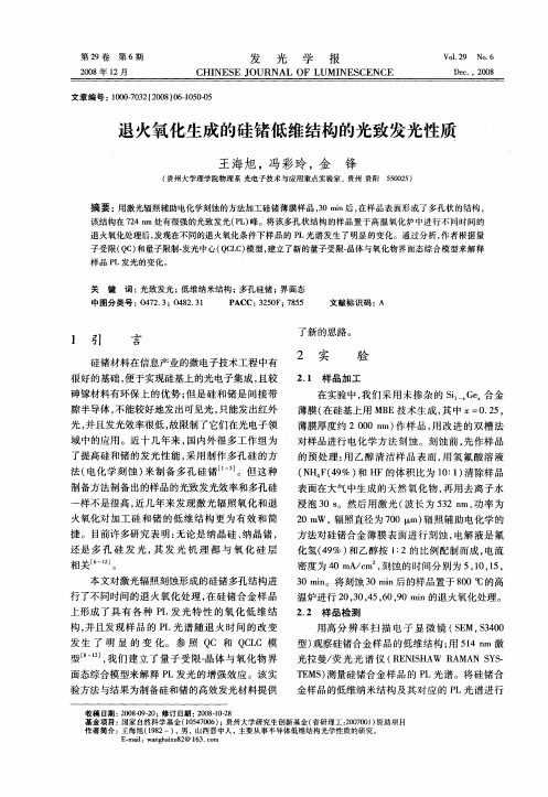
图 2 犘 犔 发光对比图 洞 壁 上 网 孔 状 结 构 处 的 犘 犔 发光比较多孔硅 犘 犔 发光的要强 2 个数量级 ( 比较可见 : 多孔硅的 犘 由此衬托出 犔 发光并不弱, 网孔状结构处的 犘 犔 发光很强 ) . 图 4 与时间相关的 犘 犔 图 开始时样品的 犘 犔发光随激光加工时间增加 而增强 ; 当激光加工时间在 9 狊时 , 犘 犔 发光最强 .
1 引言
硅与锗的材料 在 信 息 产 业 中 的 微 电 子 工 程 里 有 很 好的基础与应用 , 硅和锗的器件便于 实现 硅基上的光 电 ] 1, 2 且较砷化镓材料器件有环保上 的优势 [ ; 但是 子集成 , 硅和锗的间接跃迁能带结构使其发光 效率 较低 , 限 制了 其应用范围 , 这是目前的瓶颈难题 . 近十 几年 来 , 在 研究 硅和锗的发光性能时发现 , 其低维 结构 形成的 能带变 化 [ ] 带来很强的 犘 过去常用电化学方法来生成 犔 发 光 3~5 . [ , ] 硅和锗的低维 结 构 6 7 , 最近几年发现激光辐照方法对
) 犉 犻 . 1 ( 犪 犛 犈犕 犘 犺 狅 狋 狅狅 犳 狋 犺 犲犺 狅 犾 犲 狀 犲 狋 狊 狋 狉 狌 犮 狋 狌 狉 犲狅 犳 狊 犻 犾 犻 犮 狅 狀犳 狅 狉 犿 犵 ; ( ) 犻 狀 犲 犱 犻 狊 狋 狉 犻 犫 狌 狋 犻 狅 狀 犻 狀 狋 狋 犺 犲 犻 狀 狊 犻 犱 犲狅 犳 狋 犺 犲犺 狅 犾 犲犱 狉 犻 犾 犾 犲 犱犫 犾 犪 狊 犲 狉 犫犔 犵犪 狔 犱 犻 犪 狉 犪 犿狅 犳狅 狓 犲 狀狅 狀狋 犺 犲狊 犻 犾 犻 犮 狅 狀狊 犪 犿 犾 犲狅 犫 狋 犪 犻 狀 犲 犱犫 狊 犻 狀 犺 犲 犵 狔 犵 狆 狔狌 犵狋 犾 犻 狀 犲狊 犮 犪 狀 狀 犻 狀 犲 犮 犺 狀 犻 狌 犲狅 犳犲 犾 犲 犿 犲 狀 狋犪 狀 犪 犾 狊 犻 狊 犵狋 狇 狔
批准号 : ) 1 0 5 4 7 0 0 6 国家自然科学基金资助项目 ( : 通信作者 . 犈犿 犪 犻 犾 犠犙犎 狌 犪 狀 2 0 0 1@狔 犪 犺 狅 狅 . 犮 狅 犿 犵 0 0 7 0 3 3 1 收到 , 2 0 0 7 0 8 2 0 定稿 2 0 0 8 中国电子学会 2
第1期
黄伟其等 : 犔 发光 激光加工形成硅基上的氧化低维纳米结构的 犘
1 1 7
图 1 ( ) 洞壁上的网状低维 纳 米 硅 晶 体 结 构 的 犛 ( 洞壁上的氧 犪 犈犕 像 ; 犫) 化分布图 ( 上方的曲线为氧的成分分布 , 下方的曲线是硅的成分分布 )
图 3 脱氧加工的样品的 犘 犔 发光对比图 分别浸入酒精和氢氟酸进行激 光辐照加工的样品几乎没有 犘 水中的样品仍有一些 犘 犔 发光 , 犔 发光 .
照到样品上的 能 量 , 激光束的辐照圆斑直径调整到3 0 ; 辐照时间控制为 这时 , 在硅 样品 表面被 0 犿 8~9 狊 . ~5 μ 打出的孔洞的侧壁上形成较规则 的网 孔状 结构 , 各个网 孔由几 狀 厚的网孔壁相互隔开 , 如图 ( ) 所示 犿 1犪 . 用波长 5 直径的束斑 , 1 4 狀 犿 的激光会聚为 1 犿 犘 犔 μ 发光的区域可定位于洞壁上的网 孔状 结构 处 . 发 现该处 有很强的 犘 其强度比一般的多孔硅样品的 犘 犔 发 光, 犔 发光强度要大 2 个数量级 , 如图 2 所示 . 用电子探针元 素 线 扫 描 分 布 技 术 分 析 来 显 现 洞 壁 如图 1 ( ) 所示 ) 上的氧化程度 ( 犫 . 为了 确 定 硅 样 品 表 面 氧 化 在 增 强 犘 犔 发光上所起 的作用 , 我们设计 并 进 行 了 以 下 实 验 : 将硅样品作预处 理后 , 分别浸入酒精 、 氢氟酸和水 中进 行激 光辐照加工 ; 在保持浸泡状态中检测样品的 犘 如图 3 所示 . 这 犔 发光 , 将激光与硅样品的作用过程和检 测过 程均隔 离于无 样, 分 别 比 较 将 硅 样 品 浸 入 酒 精、 氢氟酸和 氧化的环境中 . 水中的激光加工样 品 的 犘 浸入酒精和氢氟 犔 发 光 结 果, 酸中的硅 样 品 表 面 基 本 没 有 氧 化 , 故几乎没有 犘 犔发 光; 而在水中用激 光 加 工 的 硅 样 品 表 面 情 况 较 复 杂 , 仍 故仍有较弱的 犘 有较少的氧化发生 , 犔 发光 .
8~1 0] 加工硅和锗的低维结构更为有效和简捷 [ . 目前 , 迫切需要解决的问题是 在硅和 锗样 品上 生成 稳定的低维结构并有较强且稳定的 犘 犔 发 光乃至 犈 犔发 光. 最近的研究表 明 : 无论是纳米硅晶发光还是多孔硅 发光 , 其发光机理 都 与 氧 化 硅 层 相 关 , 即所谓的纳米硅 晶的光泵作用与氧化硅层发光中心的 亚稳 态激射 . 传统 的生成纳米硅晶和氧化硅层二体系统 结构 的方法为 : 经 高温退火在富硅氧化层中形成硅原子 团簇 , 或用溅射法 将 硅 离 子 注 入 氧 化 层, 但其加工质量和稳定性都不理 想. 我们认为 : 用激光辐照手段生成纳米硅晶和氧化硅 层二体结构应该 是 最 有 希 望 的 方 法 , 包 括: 在氧化层中 用激光诱导硅离子或锗离子游离 与凝聚 、 用激 光辐 照生 成低维结构并使其表面氧化等 ; 激 光辐 照的助 氧化作 用 是很明显的 , 我们 设 计 了 相 应 的 实 验 , 例如在激光辐照 下的硅样品 3 0 0℃ 退火的氧化效 果接 近于 8 0 0℃ 的 单纯 退火的 氧 化 效 果 ; 又例如3 的 连 续 激光在硅 0犠 犢犃犌 表面辐照 2 在精密椭 0 狊能生成十几纳 米 厚 的 氧 化 硅 层 ; 偏测厚仪上增加激光束的辐照强 度 , 可 直接测 量激光辐 照时间与氧化层厚度增加的变化关 系 ; 在硅的 氧化层 中
用激光诱导能生 成 镶 嵌 于 层 中 的 纳 米 硅 或 锗 的 量 子 团 簇. 总之 , 用激光 辐 照 手 段 来 构 造 氧 化 低 维 结 构 有 独 特 的优越性 . 本文选择用激 光 辐 照 的 方 法 在 单 晶 硅 样 品 和 锗 硅 合金样品上加工出 具 有 较 强 的 、 稳定的 犘 犔 发光特性的 氧 化 低 维 结 构, 包括用不同功率的连续激光和脉冲激 乃至超快脉冲 激 光 来 加 工 样 品 , 并从物理层面上研 光、 究氧化低维结构 的 生 成 机 理 , 分 析 激 光 与 硅 材 料、 激光 建立 激光 诱导 的冷等 与锗硅合金材料的相互作用过程 , 离子体波作用模 型 , 从 而 指 导 激 光 加 工 的 优 化 过 程. 参 [ ] 1 1~1 3 模型 , 建立量子受限 晶 体与 氧化 物界面 照犙 犆 犔 犆 态综合模型来解释 犘 并设法从低维 犔 发 光 的 增 强 效 应, 纳米晶体量子受 限 态 与 氧 化 硅 界 面 态 的 相 对 位 置 来 构 造犘 从而解决所谓 犔 发光 增 强 效 应 的 阈 值 分 布 结 构, [ 1 4] “ 临界尺寸 ” 的难题 . 我们认为 : 犘 犔 发光的增强由较高 的低维纳米晶体的电子能态分布和较低的氧化硅与纳晶 界面中的界面态 分布 所交 织构成 的阈 值区 间决 定 . 不同 条件加工的不同纳米结构的晶体与氧化硅的界面态具有 不同的特征分布 , 从而产生不同频率的 犘 犔 发光分布 .
犉 犻 . 3 犠 犲 犪 犽 犲 狉犘 犔犲 犿 犻 狊 狊 犻 狅 狀狅 犳狋 犺 犲狊 犪 犿 犾 犲 狊狑 犺 犻 犮 犺狑 犲 狉 犲犻 犿 犵 狆 , , 犿 犲 狉 狊 犲 犱犻 狀犎 犉( 4 9% ) 犈 狋 犺 犪 狀 狅 犾犪 狀 犱狆 狌 狉 犲狑 犪 狋 犲 狉 狉 犲 狊 犲 犮 狋 犻 狏 犲 犾 犺 犲 狀 狆 狔狑 犻 狉 狉 犪 犱 犻 犪 狋 犲 犱
第2 9卷 第1期 2 0 0 8年1月
半 导 体 学 报
犑 犗犝犚犖犃 犔犗 犉犛 犈犕 犐 犆 犗犖犇犝犆 犜 犗犚 犛
犞 狅 犾 . 2 9 犖 狅 . 1 , 犑 犪 狀 . 2 0 0 8
激光加工形成硅基上的氧化低维纳米结构的 犘 犔 发光
1 1 1 1世荣 秦朝建 秦水介 ( ) 1 贵州大学贵州光电子技术与应用重点实验室 , 贵阳 5 5 0 0 2 5 ( ) 2 中国科学院地球化学研究所 , 贵阳 5 5 0 0 0 3
2 实验
在激光加工 中 , 辐照用的激光源有2 0~4 0 犿犠 的 由1 5 3 2 狀 犿 波长的连续 激 光 ( 0 6 4 狀 犿 波 长 的 犢犃犌 激 光 倍频产生 ) , 有1 的 0~5 0犠 1 0 6 4 狀 犿 波 长 的 犢犃犌 连 续 激光 和 对 应 的 1 0 狀 狊 脉 宽 的 脉 冲 激 光 ,还 有 1 2 0 犳 狊 ( / ) 的超快脉冲 激 光 分 别 用 单 晶 硅 和 锗 硅 合 金 1 8 0 犿 犑狆 . 作样品 . 用分子束外延( 方法或化学气相沉积 犕犅 犈) ( ) 方法生成 ( )薄膜衬底 . 犆 犞犇 犛 犻 犲 2 5 1-狓犌 狓 狓=0 用各种功率的 连 续 激 光 和 脉 冲 激 光 分 别 照 射 单 晶
硅样品或硅锗 合 金 样 品 . 当 采 用 几 十 犿犠 的 小 功 率 激 光辐照时 , 同时用 电 化 学 方 法 加 工 样 品 . 改变激光辐照 的功率 、 辐照的时 间 和 环 境 参 量 , 在各种加工的样品中 寻找稳定的 、 较强的 犘 发 光 的 氧 化 低 维 结 构. 用电子 犔 日 本 岛 津 公 司 制 造) 的扫描 扫描探 针 ( 犈 犘犕犃 1 6 0 0 型, 二次电子和背 散 射 电 子 成 像 技 术 观 察 与 分 析 样 品 的 形 貌结构 ; 并用电子扫描探针的元素 线分布 和元 素面 分布 分析技术测量样品的形貌结构对 应的成 分分 布 ; 用 英国 犚 犈 犖 犐 犛 犎犃犠 公司的 犚 犪 犿 犪 狀 光谱仪测 量样 品结 构 所 对 应的光致发光谱 . 经大量的实验 探 索 , 筛 选 出 3 种 有 价 值 的 样 品, 其 加工过程与结果描述如下 : ( )用电阻率为 1 1 0~2 0 犿 的 狆型犛 犻作 样 品 . Ω·犮 首先将 样 品 进 行 清 洗 , 然后用1 波 长 、 0 6 4 狀 犿 2 0~3 0犠 功率的 犢犃犌 连续激光辐照样品 , 辐照时间分别为 1, 2, , …, 在硅样品表面打出孔洞 3 1 5 狊 . . 控制 加 工 条 件 : 固 定 犢犃犌 激 光 的 工 作 电 流 , 使输 出功 率 为3 ; 用 特 有 的 “ 散 焦 束 斑 ” 方 法 控 制 激 光 辐 0犠