Orcad 16.5 DRC setting
OrCAD 166新功能教程

•如果元件属性中
BOM_IGNORE=TRUE 那么Capture出BOM的时候 将不包含此元件
上海库源电气科技有限公司
Web:
Forum:
PCB功能增强-节点推挤
•推挤时可编辑节点变化方式 •Line •Arc
Corner:节点增加线段
功能增强-保存
•增强保存功能, •只标示本次操作修改内容
上海库源电气科技有限公司
Web:
Forum:
功能增强-save as project
Save as project可以将工程所所涉及的库 及DSN文件等统一另存为,比之16.5中针对 Project的Save AS只保存opj文件,DSN以及 库文件无法同步另存为这个功能增强更有方便。
Cadence SPB 16.6 What’s New
Cadence SPB 16.6 新特性——OrCAD篇
上海库源电气科技有限公司
Web:
Forum:
原理图驱动的信号完整性分析
-Capture 流程
1、设置仿真条件
2、提取网络拓扑
Forum:
4、查看仿真波形
上海库源电气科技有限公司
3、在SigXplorer中仿真设置约束,并提取“TOP”
Web: Forum:
原理图驱动的信号完整性分析
-PCB 流程
上海库源电气科技有限公司
Web:
Forum:
Corner:节点增加圆弧
•Move:单纯移动节点
上海库源电气科技有限公司
Web:
Forum:
PCB功能增强-元件对齐
•在Placement
Edit编辑模式下,可以设置对齐参数,
CadenceAllegro16.5培训教程
CadenceAllegro16.5培训教程Cadence Allegro 16.5培训教程引言Cadence Allegro 16.5是一款功能强大的电子设计自动化工具,广泛应用于电子设计领域。
本文档旨在提供有关Cadence Allegro 16.5培训教程的详细信息,帮助初学者快速上手使用该工具。
第一部分:介绍1.1 Cadence Allegro 16.5概述Cadence Allegro是一款专业的PCB设计工具,提供从原理图设计到布局绘制和印制板制造的全面工作流程。
它具有强大的功能和灵活的工作环境,能够满足各类电子产品的设计需求。
1.2 Cadence Allegro 16.5的优点- 强大的功能:Cadence Allegro 16.5提供了丰富的设计工具,包括原理图绘制、版图设计、信号完整性分析等,能够满足复杂电路设计的需求。
-多种设计约束:Cadence Allegro 16.5支持多种设计约束设置,如电气约束、尺寸约束、信号完整性约束等,保证设计的可靠性和稳定性。
- 高度集成:Cadence Allegro 16.5与其他Cadence软件工具的无缝集成,如OrCAD、Allegro PCB SI等,方便设计师实现整个设计流程的协同工作。
- 内置验证机制:Cadence Allegro 16.5提供了强大的验证工具,如设计规则检查、布局识别检查等,帮助设计师快速发现和解决问题。
- 全面的制造支持:Cadence Allegro 16.5支持从布局到印制板制造的全面工作流程,包括设计生成、工艺规划、生产输出等,保证设计的可制造性和可靠性。
第二部分:基础知识2.1 Cadence Allegro 16.5界面介绍Cadence Allegro 16.5的界面由主窗口、菜单栏、工具栏、设计文件预览等组成。
本节介绍各个组件的功能和使用方法。
2.2 常用命令本节介绍Cadence Allegro 16.5中一些常用命令的使用方法,如绘制元件、连接电路、设置约束等。
Orcad16.5原理图转PADS_Logic原理图方法
Orcad16.5原理图转PADS logic原理图方法在将Cadence公司的Orcad16.5原理图文件转成PADS logic原理图时,需要经过以下三个步骤:(1)将Orcad16.5原理图文件另存为低版本Orcad16.2原理图文件,文件后缀名为.dsn;(2)在PADS logic软件中打开Orcad16.2原理图文件,并将其另存为PADS logic原理图文件,文件后缀名为.sch;转换后得到的PADS logic原理图文件除了在文件属性方面是Logic原理图文件后,其仍然具备Orcad16.2原理图文件的特点。
例如,在Orcad16.2原理图文件中存在原理图分层结构,而Logic 不存在该结构。
但是由于两种软件的原理图兼容,因此,在Orcad16.2原理图中出现的符号仍然可以在PADS logic中打开,但是PADS Logic本身可能没有该符号或者该符号异于Orcad16.2原理图符号(例如,两种软件的接地符号、电源符号、换页连接符等就不一样)。
因此,转换后得到的Logic原理图文件并不能直接使用,需要进一步修改为标准PADS logic原理图文件。
(3)在PADS logic中新建一个原理图文件,然后将转换后得到的Logic原理图文件复制到该原理图中,这时发生一个很有意思的现象:将原有Logic 原理图文件粘贴到该原理图中时,原Orcad16.2原理图符号竟然变成了Logic 本身的原理图符号(例如,接地符号、电源符号、换页连接符变成Logic原理图符号)。
在此基础上,用Logic中的元件替换转换后原理图文件中的符号即可。
将该文件进行修改并保存,即可得到最终的标准Logic原理图文件。
对于由Protel99se原理图文件转换后得到的PADS logic原理图文件,也存在上述步骤(2)提到的问题,因此也可以用上述步骤(3)来解决。
温馨提示:在将Orcad16.2原理图文件转换后得到的PADS logic原理图文件在局部一些地方跟原有Orcad16.2原理图文件有差异,这时需要对转换后得到的原理文件进行小范围修改,以保证原始设计文件在Logic中真实展现。
Orcad16.5原理图转PADS Logic原理图方法

Orcad16.5原理图转PADS logic原理图方法在将Cadence公司的Orcad16.5原理图文件转成PADS logic原理图时,需要经过以下三个步骤:(1)将Orcad16.5原理图文件另存为低版本Orcad16.2原理图文件,文件后缀名为.dsn;(2)在PADS logic软件中打开Orcad16.2原理图文件,并将其另存为PADS logic原理图文件,文件后缀名为.sch;转换后得到的PADS logic原理图文件除了在文件属性方面是Logic原理图文件后,其仍然具备Orcad16.2原理图文件的特点。
例如,在Orcad16.2原理图文件中存在原理图分层结构,而Logic 不存在该结构。
但是由于两种软件的原理图兼容,因此,在Orcad16.2原理图中出现的符号仍然可以在PADS logic中打开,但是PADS Logic本身可能没有该符号或者该符号异于Orcad16.2原理图符号(例如,两种软件的接地符号、电源符号、换页连接符等就不一样)。
因此,转换后得到的Logic原理图文件并不能直接使用,需要进一步修改为标准PADS logic原理图文件。
(3)在PADS logic中新建一个原理图文件,然后将转换后得到的Logic原理图文件复制到该原理图中,这时发生一个很有意思的现象:将原有Logic 原理图文件粘贴到该原理图中时,原Orcad16.2原理图符号竟然变成了Logic 本身的原理图符号(例如,接地符号、电源符号、换页连接符变成Logic原理图符号)。
在此基础上,用Logic中的元件替换转换后原理图文件中的符号即可。
将该文件进行修改并保存,即可得到最终的标准Logic原理图文件。
对于由Protel99se原理图文件转换后得到的PADS logic原理图文件,也存在上述步骤(2)提到的问题,因此也可以用上述步骤(3)来解决。
温馨提示:在将Orcad16.2原理图文件转换后得到的PADS logic原理图文件在局部一些地方跟原有Orcad16.2原理图文件有差异,这时需要对转换后得到的原理文件进行小范围修改,以保证原始设计文件在Logic中真实展现。
cadence16.5安装心得
cadence16.5安装心得参照论坛的安装方法,仍然碰到了一些问题,因此把安装过程记录下来,希望之后安装的朋友不走这些弯路。
破解文件请于论坛中下载。
1、点setup.exe,安装licensemanager,问license时点cancel,restart my computer later,finish。
2、安装product选择license位置时,不要5280@xxx,而是输入C:\Cadence\LicenseManager\license.dat最后finishexit3、在任务管理器关掉下面两个进程(如果有的话):cdsNameServer.execdsMsgServer.exe4、把安装目录下的SPB_16.5/tools/pspice目录下的orsimsetup.dll剪切出来放着(如果不用仿真就删掉,第8步完成后拷回,剪切到tools/pspice目录以外)5、把破解文件夹crack\licens_gen里的pubkey pubkey1.3.exe,crack里licenseManagerPubkey.bat放到Cadence/LicenseManager目录下并运行licenseManagerPubkey.bat6、把破解文件夹crack\licens_gen里的pubkey pubkey1.3.exe,crack里ToolsPubkey.bat放到Cadence/SPB_16.5/tools目录下并运行ToolsPubkey.bat7、修改crack\licens_gen\src.lic文件里面第二个word(host name)为计算机的名字删除破解文件夹licens_gen下的license.lic,然后双击licgen.bat生成新的license.lic,copy 到安装目录下适当地方,如C:\Cadence\LicenseManager\8、在开始/程序里运行LicenseManager/License server configuration Unilily,弹出窗口点browes...指向刚才生成的license.lic打开,next,将主机名改成系统hostname。
Allegro16.5新增功能(中文版)
Allegro16.5新增功能(中文版)What’s New in Cadence OrCAD PCB Designer from 15.7 to 16.5Graser -JonathanTopicUIUsability Enhancements to Allegro Applications ?Constraints HDIx Icon 的更新,及工具群組的變更x 使工具視窗最大化GUI Modernization Cadence Branding New Icons Fold-Away Window TabsApplication Modes分為General,Etch,None….模式Quick access to popular forms or functionsEditing commands associated with selected elementHierarchical parent elementsUser controlsStatus Bar UpdatesFunctional responses forClass-subclassApp modesSuper filterNumber of selected objectsGeneral Edit Application Modes pre-selection編輯模式Central Location for Design Parameters新的參數設定界面包含Display, Design, Text, Etch Edit, Shape and manufacturingNew graphics engine支援OpenGL顯示OpenGL Enabled OpenGL DisabledQuick Access to Commonly Used Subclasses 自設常用的層面Highlighting with StipplesColor Dialog is enhanced tosupport 15 stipple patternsAssign color optionsHighlight optionsHighlighting with StipplesHighlighting of FixedNets/ComponentsDifferentiation of Keepout areasRatsnets Color Displayx使用不同顏色顯示不同層面的Ratx Display Option-Top:Top-Top:Bot-Bot:BotNet Element Coloring “Nets”Worksheet Added to Color DialogHighlight and Coloring“Assign Color”Function Integrated to Pre-Selection EnvironmentPin Number Displaypin number display with top and bottom layer visibilityFlip BoardFlip/Mirror boardabout Y axis ?Simple toggle on-offcommandFlip Mode indicator ?View and Full EditcapabilityOpen GL dependent3-D GraphicsOpen GL dependentSimple toggle On-Off command ?Full board view3-D GraphicsSupport multiple windowsView micro vias, through hole vias and traces on different layers ?Pre-selection supportView one net with HDI micro via breakout3-D GraphicsMouse driven Spin, Pan, Zoom functions ?Filtered View Options。
orCAD_PADS学习笔记[1]
![orCAD_PADS学习笔记[1]](https://img.taocdn.com/s3/m/678286f7aef8941ea76e0597.png)
orCAD_PADS学习笔记--林旭OrCAD篇如何在orCAD中批量修改元器件属性?1.选择项目文件(*.dsn),点击Tools\Export Properties。
2.设置参数。
Scope:Export entire design or Library(导出全部项目或库文件)。
Contents:part Properties(器件属性)。
Mode:Export Instance Properties(使用当前属性)。
3.进入存放路径,右击导出的*.exp文件,选择用Excel打开。
4.修改表中需要修改的参数,保存并选择“是”。
5.回到原理图环境下面,点击Tools\Import Properties,导入刚保存的Excel文件,完毕。
注意:修改时不能修改或删除属性文件的第一行和每一行的第一项和第二项。
orCAD如何生成BOM表?1.选择项目文件(*.dsn),点击Tools\Bill of Materials。
2.设置参数。
Scope:Export entire design or Library(导出全部项目或库文件)。
Contents:part Properties(器件属性)。
Mode:Export Instance(Properties)(使用当前属性)。
3.Line Item Definition中:(以下为我常用的)Header:项目\t属性\t封装\t数量\t元器件编号\tCombined property string:{Item}\t{Value}\t{pcb footprint}\t{Quantity}\t{Reference}\t4.选中Open in Excel。
5.点OK就可以了。
为什么orCAD中无法输出网表?1.DRC检查时问题特征为:ERROR [NET0021] Cannot get part.[FMT0024] Ref-des not found. Possible Logical/Physical annotation conflict.[FMT0018] Errors processing intermediate file.2.问题的原因是因为使用了orCAD中的Pspice器件库。
Cadence-V16.5-图解安装步骤
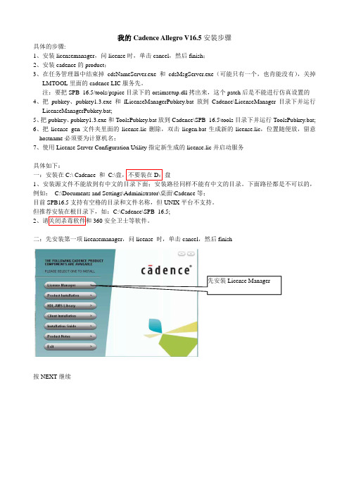
我的Cadence Allegro V16.5安装步骤具体的步骤:1、安装licensemanager ,问license 时,单击cancel ,然后finish ;2、安装cadence 的product ;3、在任务管理器中结束掉cdsNameServer.exe 和cdsMsgServer.exe (可能只有一个,也肯能没有),关掉LMTOOL 里面的cadence LIC 服务先。
注:要把SPB_16.5/tools/pspice 目录下的orsimsetup.dll 拷出来,这个patch 后是不能进行仿真设置的 4、把pubkey 、pubkey1.3.exe 和lLicenseManagerPubkey.bat 放到Cadence\LicenseManager 目录下并运行LicenseManagerPubkey.bat; 5、把pubkey 、pubkey1.3.exe 和ToolsPubkey.bat 放到Cadence\SPB_16.5\tools 目录下并运行ToolsPubkey.bat; 6、把license_gen 文件夹里面的license.lic 删除,双击licgen.bat 生成新的license.lic ,位置随便放,留意hostname 必须要为计算机名;7、使用License Server Configuration Utility 指定新生成的license.lic 并启动服务具体如下:一:安装在C:\ Cadence 和 C:\盘,不要装在D :盘1、安装源文件不能放到有中文的目录下面;安装路径同样不能有中文的目录。
下面路径都是不可以的,例如: C:\Documents and Settings\Administrator\桌面\Cadence 等; 目前SPB16.5支持有空格的目录和文件名称,但UNIX 平台不支持。
但推荐安装在根目录下,如:C:\Cadence\SPB_16.5;2、请关闭杀毒软件和360安全卫士等软件。
- 1、下载文档前请自行甄别文档内容的完整性,平台不提供额外的编辑、内容补充、找答案等附加服务。
- 2、"仅部分预览"的文档,不可在线预览部分如存在完整性等问题,可反馈申请退款(可完整预览的文档不适用该条件!)。
- 3、如文档侵犯您的权益,请联系客服反馈,我们会尽快为您处理(人工客服工作时间:9:00-18:30)。
Orcad 16.5 DRC settingDesign Rules Options tabUse thisTo do this...control...Scope Select the scope of the design rules check. The scope can cover the entire design, or selected schematic folders and pages. Mode Specify to check either instances or occurrences.Capture automatically sets this option based on the project type. Alldesigns default to use instances. If a PCB or Schematic designis complex or has occurrence properties, the default shiftsto occurrences. Capture recommends the preferred mode, whichyou can override.Action Specifies either a design rules check, deletion of existing DRC markers or creating DRC markers for warning.Note: The DRC markers are automatically deleted when you runa subsequent design rules check.Use the Ignore DRC Warnings option to specify any DRC Warningsthat you do not want to be checked during the DRC check andnetlisting. For example, to ignore the ALG0051 or ALG0016warnings during netlist, specify these in the Ignore Warningsdialog.Design Rules Select the type of rules to run, electrical and / orphysical. Report file Specify the path and file name for the report.View Output Open the design rules check report file in a text editor. Browse Displays a standard Windows dialog box for selecting files.Electrical Rules tabElectrical RulesUse this control...To do this...Check single node nets Check if the design contains any nets with only oneconnection.Check no driving sourceand Pin type conflictsCheck duplicate net names Check if the design contains any duplicate net names.Check off-page connectorconnections Verify that off-page connector nets on a schematic page match those on other schematic pages.Check hierarchical portconnections Verify that hierarchical pins in a hierarchical block match hierarchical ports in the child schematic folder or folders.Errors are generated if the number ofhierarchical ports and hierarchical pins differ between the parent and child schematic folders. Also generates errors if the types of hierarchical ports are not identical between the parent and child schematic folders.Check unconnected bus nets Check for and reports all unconnected bus nets. This check will run for all unconnected bus nets across schematics in a design.Check unconnected pins Check for any pins on the design thatare unconnected or do not have no-connect attached.Check SDT compatibility Check for SDT compatibility. For more informationabout SDT compatibility, see Saving in SDT format.ReportsUse this control...To do this...Report all net names List the names of all nets in the report file.Report off-grid objects List all objects that are on Fine grid in thereport file.Report hierarchical ports and off-page connectors List all hierarchical ports and off-page connectors in the report file.Report misleading tapconnections Checks for and reports those signals thatare wrongly connected through a Bus Tap to a bus. Also checks for missing bus taps.Physical Rules tabPhysical RulesUse this control...To do this...Check power pin visibility Check if the visibility property of a power pinon one section of multi-section part is differentfrom the corresponding power pin on anothersection of the part.Check missing/illegal PCB Footprint property Check if the PCB footprint property on a part is missing or the property defined is illegal.Check Normal Convert view sync Check if the pin numbers on the normal view of a part are different from the pin numbers on the convert view.Check incorrectPin_Groupassignment Check if all pins in same pin group in a part are of the same type.Check high speed props syntax Check the syntax of the high speed properties of the nets in the design.Check missing pin numbers Check if any part on the design has missingpin numbers.Check device with zero pins Check if any part on the design has no pin on the part.Check power ground short Check if the type of power pin name inside a part isconnected to a net on the schematic with adifferent name.Check Name Prop consistency Check if the occurrences of a hierarchical block have the same "Name" property.ReportsUse this control...To do this...Report Visible unconnected power List the names of all visible unconnectedpins power pins.Report unused part packages List the names of any unused part packages. Report invalid packaging List any invalid packaging.Report identical part references List any identical part references.ERC Matrix tabUse thisTo do this...control...Matrix Set the rules used by the Design Rules Check when testing connections between pins, hierarchical blocks, andhierarchical ports.The pins, hierarchical ports, and off-page connectors arelisted in columns and rows in the table. A test is representedby the intersection of a row and column. Either theintersection of a row and column is empty, or it contains a"W" or an "E." An empty intersection represents a validconnection, a "W" is a warning, and an "E" represents an error.You can cycle through these three settings by pointing to anintersection and clicking the mouse button until the desiredsetting displays. You can also type W for warning, E for error,and N for an empty intersection. In addition to these keys,you can use the arrow keys to select other intersections. RestoreRestore the ERC matrix to its default values.defaults。