SN74AC533DWG4中文资料
74LS240中文资料

LOW POWER SCHOTTKYDevice Package Shipping SN74LS240N 16 Pin DIP 1440 Units/Box SN74LS240DW 16 Pin SOIC DW SUFFIX CASE 751D2500/T ape & Reel PLASTIC N SUFFIX CASE 738201201SN74LS244N 16 Pin DIP 1440 Units/Box SN74LS244DW16 Pin2500/T ape & ReelON Semiconductor and are trademarks of Semiconductor Components Industries, LLC (SCILLC). SCILLC reserves the right to make changes without further notice to any products herein. SCILLC makes no warranty, representation or guarantee regarding the suitability of its products for any particular purpose, nor does SCILLC assume any liability arising out of the application or use of any product or circuit, and specifically disclaims any and all liability, including without limitation special, consequential or incidental damages. “Typical” parameters which may be provided in SCILLC data sheets and/or specifications can and do vary in different applications and actual performance may vary over time. All operating parameters, including “Typicals” must be validated for each customer application by customer’s technical experts. SCILLC does not convey any license under its patent rights nor the rights of others.SCILLC products are not designed, intended, or authorized for use as components in systems intended for surgical implant into the body, or other applications intended to support or sustain life, or for any other application in which the failure of the SCILLC product could create a situation where personal injury or death may occur. Should Buyer purchase or use SCILLC products for any such unintended or unauthorized application, Buyer shall indemnify and hold SCILLC and its officers, employees, subsidiaries, affiliates, and distributors harmless against all claims, costs, damages, and expenses, and reasonable attorney fees arising out of, directly or indirectly, any claim of personal injury or death associated with such unintended or unauthorized use, even if such claim alleges that SCILLC was negligent regarding the design or manufacture of the part. SCILLC is an Equal Opportunity/Affirmative Action Employer. PUBLICATION ORDERING INFORMATIONASIA/PACIFIC: LDC for ON Semiconductor – Asia SupportPhone:303–675–2121 (Tue–Fri 9:00am to 1:00pm, Hong Kong Time)Toll Free from Hong Kong 800–4422–3781Email: ONlit–asia@JAPAN: ON Semiconductor, Japan Customer Focus Center4–32–1 Nishi–Gotanda, Shinagawa–ku, Tokyo, Japan 141–8549Phone: 81–3–5487–8345Email: r14153@Fax Response Line:303–675–2167。
MC74AC240DWG资料

MC74AC240, MC74ACT240Octal Buffer/Line Driver with 3−State OutputsThe MC74AC240/74ACT240 is an octal buffer and line driver designed to be employed as a memory address driver, clock driver and bus oriented transmitter or receiver which provides improved PC board density.Features•3−State Outputs Drive Bus Lines or Buffer Memory Address Registers•Outputs Source/Sink 24 mA•′ACT240 Has TTL Compatible Inputs •Pb−Free Packages are AvailableTRUTH TABLEInputs Outputs OE 1D (Pins 12, 14, 16, 18)L L H L H L H XZNOTE:H = HIGH Voltage Level L = LOW Voltage Level X = ImmaterialZ = High ImpedanceTRUTH TABLEInputs Outputs OE 2D (Pins 3, 5, 7, 9)L L H L H L H XZNOTE:H = HIGH Voltage Level L = LOW Voltage Level X = ImmaterialZ = High ImpedanceV OE OE 1GNDFigure 1. Pinout: 20−Lead Packages Conductors(Top View)SOIC−20W DW SUFFIX CASE 751DTSSOP−20DT SUFFIX CASE 948ESOEIAJ−20M SUFFIX CASE 9671PDIP−20N SUFFIX CASE 738See detailed ordering and shipping information in the package dimensions section on page 6 of this data sheet.ORDERING INFORMATIONSee general marking information in the device marking section on page 7 of this data sheet.DEVICE MARKING INFORMATIONMAXIMUM RATINGSSymbol Parameter Value Unit V CC DC Supply Voltage (Referenced to GND)−0.5 to +7.0V V IN DC Input Voltage (Referenced to GND)−0.5 to V CC +0.5V V OUT DC Output Voltage (Referenced to GND)−0.5 to V CC +0.5VI IN DC Input Current, per Pin±20mAI OUT DC Output Sink/Source Current, per Pin±50mAI CC DC V CC or GND Current per Output Pin±50mAT stg Storage Temperature−65 to +150°C Stresses exceeding Maximum Ratings may damage the device. Maximum Ratings are stress ratings only. Functional operation above the Recommended Operating Conditions is not implied. Extended exposure to stresses above the Recommended Operating Conditions may affect device reliability.RECOMMENDED OPERATING CONDITIONSSymbol Parameter Min Typ Max UnitV CC Supply Voltage ′AC 2.0 5.0 6.0V ′ACT 4.5 5.0 5.5V IN, V OUT DC Input Voltage, Output Voltage (Ref. to GND)0−V CC Vt r, t f Input Rise and Fall Time (Note 1)′AC Devices except Schmitt InputsV CC @ 3.0 V−150−V CC @ 4.5 V−40−ns/VV CC @ 5.5 V−25−t r, t f Input Rise and Fall Time (Note 2)′ACT Devices except Schmitt InputsV CC @ 4.5 V−10−ns/VV CC @ 5.5 V−8.0−T J Junction Temperature (PDIP)−−140°C T A Operating Ambient Temperature Range−402585°CI OH Output Current − High−−−24mAI OL Output Current − Low−−24mA1.V IN from 30% to 70% V CC; see individual Data Sheets for devices that differ from the typical input rise and fall times.2.V IN from 0.8 V to 2.0 V; see individual Data Sheets for devices that differ from the typical input rise and fall times.DC CHARACTERISTICSSymbol Parameter V CC(V)74AC74ACUnit Conditions T A = +25°C T A =−40°C to +85°CTyp Guaranteed LimitsV IH Minimum High LevelInput Voltage 3.0 1.5 2.1 2.1V OUT = 0.1 V4.5 2.25 3.15 3.15V or V CC − 0.1 V5.5 2.75 3.85 3.85V IL Maximum Low LevelInput Voltage 3.0 1.50.90.9V OUT = 0.1 V4.5 2.25 1.35 1.35V or V CC − 0.1 V5.5 2.75 1.65 1.65V OH Minimum High LevelOutput Voltage 3.0 2.99 2.9 2.9I OUT = −50 m A4.5 4.49 4.4 4.4V5.5 5.49 5.4 5.4V*V IN = V IL or V IH3.0− 2.56 2.46−12 mA4.5− 3.86 3.76I OH−24 mA5.5− 4.86 4.76−24 mAV OL Maximum Low LevelOutput Voltage 3.00.0020.10.1I OUT = 50 m A4.50.0010.10.1V5.50.0010.10.1V*V IN = V IL or V IH3.0−0.360.4412 mA4.5−0.360.44I OL24 mA5.5−0.360.4424 mAI IN Maximum InputLeakage Current5.5−±0.1±1.0m A V I = V CC, GNDI OZ Maximum3−StateCurrentV I(OE) = V IL, V IH 5.5−±0.5±5.0m A V I = V CC, GNDV O = V CC, GNDI OLD†Minimum DynamicOutput Current 5.5−−75mA V OLD = 1.65 V MaxI OHD 5.5−−−75mA V OHD = 3.85 V MinI CC Maximum QuiescentSupply Current5.5−8.080m A V IN = V CC or GND*All outputs loaded; thresholds on input associated with output under test.†Maximum test duration 2.0 ms, one output loaded at a time.NOTE:I IN and I CC @ 3.0 V are guaranteed to be less than or equal to the respective limit @ 5.5 V V CC.AC CHARACTERISTICS(For Figures and Waveforms − See AND8277/D at )Symbol Parameter V CC*(V)74AC74ACUnitFig.No.T A = +25°CC L = 50 pFT A = −40°Cto +85°CC L = 50 pFMin Typ Max Min Maxt PLH Propagation Delay 3.3 1.5 6.08.0 1.09.0ns3−5 Data to Output 5.0 1.5 4.5 6.5 1.07.0t PHL Propagation Delay 3.3 1.5 5.58.0 1.08.5ns3−5 Data to Output 5.0 1.5 4.5 6.0 1.0 6.5t PZH Output Enable Time 3.3 1.5 6.010.5 1.011.0ns3−7 5.0 1.5 5.07.0 1.08.0t PZL Output Enable Time 3.3 1.57.010.0 1.011.0ns3−8 5.0 1.5 5.58.0 1.08.5t PHZ Output Disable Time 3.3 1.57.010.0 1.010.5ns3−7 5.0 1.5 6.59.0 1.09.5t PLZ Output Disable Time 3.3 1.57.510.5 1.011.5ns3−8 5.0 1.5 6.59.0 1.09.5*Voltage Range 3.3 V is 3.3 V ±0.3 V. Voltage Range 5.0 V is 5.0 V ±0.5 V. DC CHARACTERISTICSSymbol Parameter V CC(V)74ACT74ACTUnit Conditions T A = +25°C T A = −40°C to +85°CTyp Guaranteed LimitsV IH Minimum High LevelInput Voltage 4.5 1.5 2.0 2.0VV OUT = 0.1 V 5.5 1.5 2.0 2.0or V CC − 0.1 VV IL Maximum Low LevelInput Voltage 4.5 1.50.80.8VV OUT = 0.1 V 5.5 1.50.80.8or V CC − 0.1 VV OH Minimum High LevelOutput Voltage 4.5 4.49 4.4 4.4VI OUT = −50 m A5.5 5.49 5.4 5.4*V IN = V IL or V IH4.5− 3.86 3.76V I OH−24 mA5.5− 4.86 4.76−24 mAV OL Maximum Low LevelOutput Voltage 4.50.0010.10.1VI OUT = 50 m A5.50.0010.10.1*V IN = V IL or V IH4.5−0.360.44VI OL24 mA 5.5−0.360.4424 mAI IN Maximum InputLeakage Current5.5−±0.1±1.0m A V I = V CC, GNDD I CCT Additional Max. I CC/Input 5.50.6− 1.5mA V I = V CC −2.1 VI OZ Maximum3−StateCurrentV I(OE) = V IL, V IH 5.5−±0.5±5.0m A V I = V CC, GNDV O = V CC, GNDI OLD†Minimum DynamicOutput Current 5.5−−75mA V OLD = 1.65 V MaxI OHD 5.5−−−75mA V OHD = 3.85 V MinI CC Maximum QuiescentSupply Current5.5−8.080m A V IN = V CC or GND*All outputs loaded; thresholds on input associated with output under test.†Maximum test duration 2.0 ms, one output loaded at a time.AC CHARACTERISTICS(For Figures and Waveforms − See Section 3 of the ON Semiconductor FACT Data Book, DL138/D)Symbol Parameter V CC*(V)74ACT74ACTUnitFig.No.T A = +25°CC L = 50 pFT A = −40°Cto +85°CC L = 50 pFMin Typ Max Min Maxt PLH Propagation Delay Data to Output 5.0 1.5 6.08.5 1.59.5ns3−5 t PHL Propagation Delay Data to Output 5.0 1.5 5.57.5 1.58.5ns3−5 t PZH Output Enable Time 5.0 1.57.08.5 1.09.5ns3−7 t PZL Output Enable Time 5.0 2.07.09.5 1.510.5ns3−8 t PHZ Output Disable Time 5.0 2.08.09.5 2.010.5ns3−7 t PLZ Output Disable Time 5.0 2.5 6.510.0 2.010.5ns3−8 *Voltage Range 5.0 V is 5.0 V ±0.5 V.CAPACITANCESymbol Parameter ValueTypUnit Test ConditionsC IN Input Capacitance 4.5pF V CC = 5.0 V C PD Power Dissipation Capacitance45pF V CC = 5.0 VORDERING INFORMATIONDevicePackage Shipping †MC74AC240N PDIP−2018 Units / Rail MC74AC240NG PDIP−20(Pb−Free)MC74ACT240N PDIP−20MC74ACT240NG PDIP−20(Pb−Free)MC74AC240DW SOIC−2038 Units / Rail MC74AC240DWG SOIC−20(Pb−Free)MC74AC240DWR2SOIC−201000 / Tape & Reel MC74AC240DWR2G SOIC−20(Pb−Free)MC74ACT240DW SOIC−2038 Units / Rail MC74ACT240DWG SOIC−20(Pb−Free)MC74ACT240DWR2SOIC−201000 / Tape & Reel MC74ACT240DWR2G SOIC−20(Pb−Free)MC74AC240DTR2TSSOP−20*2500 / Tape & Reel MC74AC240DTR2G TSSOP−20*MC74ACT240DTR2TSSOP−20*MC74ACT240DTR2G TSSOP−20*MC74AC240MEL SOEIAJ−202000 / Tape & Reel MC74AC240MELG SOEIAJ−20(Pb−Free)MC74ACT240MEL SOEIAJ−202000 / Tape & Reel MC74ACT240MELGSOEIAJ−20(Pb−Free)†For information on tape and reel specifications, including part orientation and tape sizes, please refer to our Tape and Reel Packaging Specifications Brochure, BRD8011/D.*These packages are inherently Pb−Free.MARKING DIAGRAMSPDIP−20SOIC−20W TSSOP−20SOEIAJ−20201120AC 240ALYW G G74ACT240AWLYWWGA = Assembly Location WL, L = Wafer Lot YY, Y = YearWW, W = Work Week G or G = Pb−Free Package(Note: Microdot may be in either location)20174AC240AWLYWWG120ACT 240ALYW G GPACKAGE DIMENSIONSPDIP−20N SUFFIXPLASTIC DIP PACKAGECASE 738−03ISSUE ENOTES:1.DIMENSIONING AND TOLERANCING PER ANSI Y14.5M, 1982.2.CONTROLLING DIMENSION: INCH.3.DIMENSION L TO CENTER OF LEAD WHEN FORMED PARALLEL.4.DIMENSION B DOES NOT INCLUDE MOLD FLASH.DIM MIN MAX MIN MAX MILLIMETERSINCHES A 25.6627.171.010 1.070B 6.10 6.600.2400.260C 3.81 4.570.1500.180D 0.390.550.0150.022G 2.54 BSC 0.100 BSC J 0.210.380.0080.015K 2.80 3.550.1100.140L 7.62 BSC 0.300 BSC M 0 15 0 15 N0.51 1.010.0200.040____E 1.27 1.770.0500.070F 1.27 BSC 0.050 BSC SOIC−20WDW SUFFIX CASE 751D−05ISSUE GPACKAGE DIMENSIONSTSSOP−20DT SUFFIX CASE 948E−02ISSUE CDIM A MIN MAX MIN MAX INCHES 6.600.260MILLIMETERS B 4.30 4.500.1690.177C 1.200.047D 0.050.150.0020.006F 0.500.750.0200.030G 0.65 BSC 0.026 BSCH 0.270.370.0110.015J 0.090.200.0040.008J10.090.160.0040.006K 0.190.300.0070.012K10.190.250.0070.010L 6.40 BSC 0.252 BSC M 0 8 0 8 ____1.DIMENSIONING AND TOLERANCING PER ANSI Y14.5M, 1982.2.CONTROLLING DIMENSION:MILLIMETER.3.DIMENSION A DOES NOT INCLUDE MOLD FLASH, PROTRUSIONS OR GATE BURRS. MOLD FLASH OR GATE BURRS SHALL NOT EXCEED 0.15 (0.006) PER SIDE.4.DIMENSION B DOES NOT INCLUDE INTERLEAD FLASH OR PROTRUSION.INTERLEAD FLASH OR PROTRUSIONSHALL NOT EXCEED 0.25 (0.010) PER SIDE.5.DIMENSION K DOES NOT INCLUDE DAMBAR PROTRUSION. ALLOWABLE DAMBAR PROTRUSION SHALL BE 0.08(0.003) TOTAL IN EXCESS OF THE K DIMENSION AT MAXIMUM MATERIAL CONDITION.6.TERMINAL NUMBERS ARE SHOWN FOR REFERENCE ONLY .7.DIMENSION A AND B ARE TO BE DETERMINED AT DATUM PLANE −W−.6.400.252−−−−−−16X0.360.65PITCH*For additional information on our Pb−Free strategy and soldering details, please download the ON Semiconductor Soldering and Mounting Techniques Reference Manual, SOLDERRM/D.SOLDERING FOOTPRINT*PACKAGE DIMENSIONSSOEIAJ−20M SUFFIX CASE 967−01ISSUE ADIM MIN MAX MIN MAX INCHES−−− 2.05−−−0.081MILLIMETERS 0.050.200.0020.0080.350.500.0140.0200.150.250.0060.01012.3512.800.4860.5045.10 5.450.2010.2151.27 BSC 0.050 BSC 7.408.200.2910.3230.500.850.0200.0331.10 1.500.0430.0590 0.700.900.0280.035−−−0.81−−−0.032A 1H E Q 1L E _10 _0 _10 _NOTES:1.DIMENSIONING AND TOLERANCING PER ANSIY14.5M, 1982.2.CONTROLLING DIMENSION: MILLIMETER.3.DIMENSIONS D AND E DO NOT INCLUDEMOLD FLASH OR PROTRUSIONS AND AREMEASURED AT THE PARTING LINE. MOLD FLASH OR PROTRUSIONS SHALL NOT EXCEED 0.15(0.006) PER SIDE.4.TERMINAL NUMBERS ARE SHOWN FORREFERENCE ONLY.5.THE LEAD WIDTH DIMENSION (b) DOES NOTINCLUDE DAMBAR PROTRUSION. ALLOWABLE DAMBAR PROTRUSION SHALL BE 0.08 (0.003)TOTAL IN EXCESS OF THE LEAD WIDTHDIMENSION AT MAXIMUM MATERIAL CONDITION.DAMBAR CANNOT BE LOCATED ON THE LOWER RADIUS OR THE FOOT. MINIMUM SPACEBETWEEN PROTRUSIONS AND ADJACENT LEAD TO BE 0.46 ( 0.018).A b c D E e L M ZON Semiconductor and are registered trademarks of Semiconductor Components Industries, LLC (SCILLC). SCILLC reserves the right to make changes without further notice to any products herein. SCILLC makes no warranty, representation or guarantee regarding the suitability of its products for any particular purpose, nor does SCILLC assume any liability arising out of the application or use of any product or circuit, and specifically disclaims any and all liability, including without limitation special, consequential or incidental damages.“Typical” parameters which may be provided in SCILLC data sheets and/or specifications can and do vary in different applications and actual performance may vary over time. All operating parameters, including “Typicals” must be validated for each customer application by customer’s technical experts. SCILLC does not convey any license under its patent rights nor the rights of others. SCILLC products are not designed, intended, or authorized for use as components in systems intended for surgical implant into the body, or other applications intended to support or sustain life, or for any other application in which the failure of the SCILLC product could create a situation where personal injury or death may occur. Should Buyer purchase or use SCILLC products for any such unintended or unauthorized application, Buyer shall indemnify and hold SCILLC and its officers, employees, subsidiaries, affiliates,and distributors harmless against all claims, costs, damages, and expenses, and reasonable attorney fees arising out of, directly or indirectly, any claim of personal injury or death associated with such unintended or unauthorized use, even if such claim alleges that SCILLC was negligent regarding the design or manufacture of the part. SCILLC is an Equal Opportunity/Affirmative Action Employer. This literature is subject to all applicable copyright laws and is not for resale in any manner.PUBLICATION ORDERING INFORMATION。
HD74AC153T中文资料

HD74AC153Dual 4-Input MultiplexerADE-205-370 (Z)1st. EditionSep. 2000 DescriptionThe HD74AC153 is a high-speed dual 4-input multiplexer with common select inputs and individual enable inputs for each section. It can select two lines of data from four sources. The two buffered outputs present data in the true (noninverted) form. In addition to multiplexer operation, the HD74AC153 can act as a function generator and generate any two functions of three variables.Feature• Outputs Source/Sink 24 mAPin ArrangementHD74AC1532Logic SymbolPin NamesI 0a to I 3a Side A Data Inputs I 0b to I 3b Side B Data Inputs S 0, S 1Common Select Inputs E a Side A Enable Input E b Side B Enable Input Z a Side A Output Z bSide B OutputFunctional DescriptionThe HD74AC153 is a dual 4-input multiplexer. It can select two bits of data from up to four sources under the control of the common Select inputs (S 0, S 1). The two 4-input multiplexer circuits have individual active-Low Enables (E a , E b ) which can be used to strobe the outputs independently. When the Enables (E a ,E b ) are High, the corresponding outputs (Z a , Z b ) are forced Low. The HD74AC153 is the logic implementation of a 2-pole, 4-position switch, where the position of the switch is determined by the logic levels supplied to the two Select inputs. The logic equations for the outputs are shown below.Z a = E a •(I 0a •S 1•S 0 + I 1a •S 1•S 0 + I 2a •S 1•S 0 + I 3a •S 1•S 0)Z b = E b •(I 0b •S 1•S 0 + I 1b •S 1•S 0 + I 2b •S 1•S 0 + I 3b •S 1•S 0)HD74AC1533Truth TableSelect Inputs Input (a or b)Output S 0S 1E I 0I 1I 2I 3Z X X H X X X X L L L L L X X X L L L L H X X X H H L L X L X X L H L L X H X X H L H L X X L X L L H L X X H X H H H L X X X L L H HLXXXHHH :High Voltage Level L :Low Voltage Level X :ImmaterialHD74AC1534Logic DiagramDC Characteristics (unless otherwise specified)ItemSymbol Max Unit ConditionMaximum quiescent supply current I CC 80µA V IN = V CC or ground, V CC = 5.5 V,Ta = Worst caseMaximum quiescent supply currentI CC8.0µAV IN = V CC or ground, V CC = 5.5 V,Ta = 25°CHD74AC1535AC Characteristics: HD74AC153Ta = +25°C C L = 50 pFTa = –40°C to +85°C C L = 50 pF ItemSymbol V CC (V)*1Min Typ Max Min Max Unit Propagation delay t PLH3.3 1.09.515.0 1.017.5nsS n to Z n5.0 1.06.511.0 1.012.5Propagation delay t PHL 3.3 1.08.514.5 1.016.5ns S n to Z n5.0 1.06.511.0 1.012.0Propagation delay t PLH 3.3 1.08.013.5 1.016.0ns E n to Z n5.0 1.0 5.59.5 1.011.0Propagation delay t PHL 3.3 1.07.011.0 1.012.5ns E n to Z n5.0 1.0 5.08.0 1.09.0Propagation delay t PLH 3.3 1.07.512.5 1.014.5ns I n to Z n5.0 1.0 5.59.0 1.010.5Propagation delay t PHL 3.3 1.07.011.5 1.013.0ns I n to Z n 5.01.05.08.51.010.0Note:1.Voltage Range 3.3 is 3.3 V ± 0.3 VVoltage Range 5.0 is 5.0 V ± 0.5 VCapacitanceItemSymbol Typ Unit Condition Input capacitanceC IN 4.5pF V CC = 5.5 V Power dissipation capacitanceC PD65.0pFV CC = 5.0 VHD74AC153 Package Dimensions6HD74AC1537HD74AC1538Cautions1.Hitachi neither warrants nor grants licenses of any rights of Hitachi’s or any third party’s patent,copyright, trademark, or other intellectual property rights for information contained in this document.Hitachi bears no responsibility for problems that may arise with third party’s rights, includingintellectual property rights, in connection with use of the information contained in this document.2.Products and product specifications may be subject to change without notice. Confirm that you have received the latest product standards or specifications before final design, purchase or use.3.Hitachi makes every attempt to ensure that its products are of high quality and reliability. However,contact Hitachi’s sales office before using the product in an application that demands especially high quality and reliability or where its failure or malfunction may directly threaten human life or cause risk of bodily injury, such as aerospace, aeronautics, nuclear power, combustion control, transportation,traffic, safety equipment or medical equipment for life support.4.Design your application so that the product is used within the ranges guaranteed by Hitachi particularly for maximum rating, operating supply voltage range, heat radiation characteristics, installationconditions and other characteristics. Hitachi bears no responsibility for failure or damage when used beyond the guaranteed ranges. Even within the guaranteed ranges, consider normally foreseeable failure rates or failure modes in semiconductor devices and employ systemic measures such as fail-safes, so that the equipment incorporating Hitachi product does not cause bodily injury, fire or other consequential damage due to operation of the Hitachi product.5.This product is not designed to be radiation resistant.6.No one is permitted to reproduce or duplicate, in any form, the whole or part of this document without written approval from Hitachi.7.Contact Hitachi’s sales office for any questions regarding this document or Hitachi semiconductor products.Hitachi, Ltd.Semiconductor & Integrated Circuits.Nippon Bldg., 2-6-2, Ohte-machi, Chiyoda-ku, Tokyo 100-0004, Japan Tel: Tokyo (03) 3270-2111 Fax: (03) 3270-5109Copyright © Hitachi, Ltd., 2000. All rights reserved. Printed in Japan.Hitachi Asia Ltd. Hitachi Tower16 Collyer Quay #20-00, Singapore 049318Tel : <65>-538-6533/538-8577 Fax : <65>-538-6933/538-3877URL : .sg URLNorthAmerica : /Europe : /hel/ecg Asia : Japan : http://www.hitachi.co.jp/Sicd/indx.htmHitachi Asia Ltd.(Taipei Branch Office)4/F, No. 167, Tun Hwa North Road, Hung-Kuo Building, Taipei (105), Taiwan Tel : <886>-(2)-2718-3666 Fax : <886>-(2)-2718-8180 Telex : 23222 HAS-TPURL : Hitachi Asia (Hong Kong) Ltd. Group III (Electronic Components) 7/F., North Tower, World Finance Centre,Harbour City, Canton Road Tsim Sha Tsui, Kowloon, Hong KongTel : <852>-(2)-735-9218 Fax : <852>-(2)-730-0281URL : Hitachi Europe Ltd.Electronic Components Group.Whitebrook ParkLower Cookham Road MaidenheadBerkshire SL6 8YA, United Kingdom Tel: <44> (1628) 585000Fax: <44> (1628) 585160Hitachi Europe GmbHElectronic Components Group Dornacher Stra βe 3D-85622 Feldkirchen, Munich GermanyTel: <49> (89) 9 9180-0Fax: <49> (89) 9 29 30 00Hitachi Semiconductor (America) Inc.179 East Tasman Drive,San Jose,CA 95134 Tel: <1> (408) 433-1990Fax: <1>(408) 433-0223For further information write to:Colophon 2.0。
SN74LS623DWE4,SN74LS623DWG4,SN74LS623DWR,SN74LS623DWRE4,SN74LS623NSR, 规格书,Datasheet 资料

IMPORTANT NOTICETexas Instruments (TI) reserves the right to make changes to its products or to discontinue any semiconductor product or service without notice, and advises its customers to obtain the latest version of relevant information to verify, before placing orders, that the information being relied on is current.TI warrants performance of its semiconductor products and related software to the specifications applicable at the time of sale in accordance with TI’s standard warranty. Testing and other quality control techniques are utilized to the extent TI deems necessary to support this warranty. Specific testing of all parameters of each device is not necessarily performed, except those mandated by government requirements.Certain applications using semiconductor products may involve potential risks of death, personal injury, or severe property or environmental damage (“Critical Applications”).TI SEMICONDUCTOR PRODUCTS ARE NOT DESIGNED, INTENDED, AUTHORIZED, OR WARRANTED TO BE SUITABLE FOR USE IN LIFE-SUPPORT APPLICATIONS, DEVICES OR SYSTEMS OR OTHER CRITICAL APPLICATIONS.Inclusion of TI products in such applications is understood to be fully at the risk of the customer. Use of TI products in such applications requires the written approval of an appropriate TI officer. Questions concerning potential risk applications should be directed to TI through a local SC sales office.In order to minimize risks associated with the customer’s applications, adequate design and operating safeguards should be provided by the customer to minimize inherent or procedural hazards.TI assumes no liability for applications assistance, customer product design, software performance, or infringement of patents or services described herein. Nor does TI warrant or represent that any license, either express or implied, is granted under any patent right, copyright, mask work right, or other intellectual property right of TI covering or relating to any combination, machine, or process in which such semiconductor products or services might be or are used.Copyright © 1996, Texas Instruments IncorporatedTAPE AND REEL INFORMATION*All dimensions are nominalDevicePackage Type Package Drawing Pins SPQReel Diameter (mm)Reel Width W1(mm)A0(mm)B0(mm)K0(mm)P1(mm)W (mm)Pin1Quadrant SN74LS623DWR SOIC DW 202000330.024.410.813.0 2.712.024.0Q1SN74LS623NSRSONS202000330.024.48.213.02.512.024.0Q1*All dimensions are nominalDevice Package Type Package Drawing Pins SPQ Length(mm)Width(mm)Height(mm) SN74LS623DWR SOIC DW202000346.0346.041.0 SN74LS623NSR SO NS202000346.0346.041.0IMPORTANT NOTICETexas Instruments Incorporated and its subsidiaries(TI)reserve the right to make corrections,modifications,enhancements,improvements, and other changes to its products and services at any time and to discontinue any product or service without notice.Customers should obtain the latest relevant information before placing orders and should verify that such information is current and complete.All products are sold subject to TI’s terms and conditions of sale supplied at the time of order acknowledgment.TI warrants performance of its hardware products to the specifications applicable at the time of sale in accordance with TI’s standard warranty.Testing and other quality control techniques are used to the extent TI deems necessary to support this warranty.Except where mandated by government requirements,testing of all parameters of each product is not necessarily performed.TI assumes no liability for applications assistance or customer product design.Customers are responsible for their products and applications using TI components.To minimize the risks associated with customer products and applications,customers should provide adequate design and operating safeguards.TI does not warrant or represent that any license,either express or implied,is granted under any TI patent right,copyright,mask work right, or other TI intellectual property right relating to any combination,machine,or process in which TI products or services are rmation published by TI regarding third-party products or services does not constitute a license from TI to use such products or services or a warranty or endorsement e of such information may require a license from a third party under the patents or other intellectual property of the third party,or a license from TI under the patents or other intellectual property of TI.Reproduction of TI information in TI data books or data sheets is permissible only if reproduction is without alteration and is accompanied by all associated warranties,conditions,limitations,and notices.Reproduction of this information with alteration is an unfair and deceptive business practice.TI is not responsible or liable for such altered rmation of third parties may be subject to additional restrictions.Resale of TI products or services with statements different from or beyond the parameters stated by TI for that product or service voids all express and any implied warranties for the associated TI product or service and is an unfair and deceptive business practice.TI is not responsible or liable for any such statements.TI products are not authorized for use in safety-critical applications(such as life support)where a failure of the TI product would reasonably be expected to cause severe personal injury or death,unless officers of the parties have executed an agreement specifically governing such use.Buyers represent that they have all necessary expertise in the safety and regulatory ramifications of their applications,and acknowledge and agree that they are solely responsible for all legal,regulatory and safety-related requirements concerning their products and any use of TI products in such safety-critical applications,notwithstanding any applications-related information or support that may be provided by TI.Further,Buyers must fully indemnify TI and its representatives against any damages arising out of the use of TI products in such safety-critical applications.TI products are neither designed nor intended for use in military/aerospace applications or environments unless the TI products are specifically designated by TI as military-grade or"enhanced plastic."Only products designated by TI as military-grade meet military specifications.Buyers acknowledge and agree that any such use of TI products which TI has not designated as military-grade is solely at the Buyer's risk,and that they are solely responsible for compliance with all legal and regulatory requirements in connection with such use. TI products are neither designed nor intended for use in automotive applications or environments unless the specific TI products are designated by TI as compliant with ISO/TS16949requirements.Buyers acknowledge and agree that,if they use any non-designated products in automotive applications,TI will not be responsible for any failure to meet such requirements.Following are URLs where you can obtain information on other Texas Instruments products and application solutions:Products ApplicationsAmplifiers AudioData Converters AutomotiveDLP®Products BroadbandDSP Digital ControlClocks and Timers MedicalInterface MilitaryLogic Optical NetworkingPower Mgmt SecurityMicrocontrollers TelephonyRFID Video&ImagingRF/IF and ZigBee®Solutions WirelessMailing Address:Texas Instruments,Post Office Box655303,Dallas,Texas75265Copyright©2009,Texas Instruments Incorporated。
SN74HC573A中文资料
PACKAGING INFORMATIONOrderable Device Status(1)PackageType PackageDrawingPins PackageQtyEco Plan(2)Lead/Ball Finish MSL Peak Temp(3)5962-8512801VRA ACTIVE CDIP J201None Call TI Level-NC-NC-NC 5962-8512801VSA ACTIVE CFP W201None Call TI Level-NC-NC-NC 85128012A ACTIVE LCCC FK201None Call TI Level-NC-NC-NC 8512801RA ACTIVE CDIP J201None Call TI Level-NC-NC-NC 8512801SA ACTIVE CFP W201None Call TI Level-NC-NC-NC JM38510/65406BRA ACTIVE CDIP J201None Call TI Level-NC-NC-NC SN54HC573AJ ACTIVE CDIP J201None Call TI Level-NC-NC-NCSN74HC573ADBR ACTIVE SSOP DB202000Pb-Free(RoHS)CU NIPDAU Level-2-260C-1YEAR/Level-1-235C-UNLIMSN74HC573ADW ACTIVE SOIC DW2025Pb-Free(RoHS)CU NIPDAU Level-2-250C-1YEAR/Level-1-235C-UNLIMSN74HC573ADWR ACTIVE SOIC DW202000Pb-Free(RoHS)CU NIPDAU Level-2-250C-1YEAR/Level-1-235C-UNLIMSN74HC573AN ACTIVE PDIP N2020Pb-Free(RoHS)CU NIPDAU Level-NC-NC-NCSN74HC573AN3OBSOLETE PDIP N20None Call TI Call TISN74HC573APWLE OBSOLETE TSSOP PW20None Call TI Call TISN74HC573APWR ACTIVE TSSOP PW202000Pb-Free(RoHS)CU NIPDAU Level-1-250C-UNLIMSN74HC573APWT ACTIVE TSSOP PW20250Pb-Free(RoHS)CU NIPDAU Level-1-250C-UNLIM SNJ54HC573AFK ACTIVE LCCC FK201None Call TI Level-NC-NC-NC SNJ54HC573AJ ACTIVE CDIP J201None Call TI Level-NC-NC-NC SNJ54HC573AW ACTIVE CFP W201None Call TI Level-NC-NC-NC (1)The marketing status values are defined as follows:ACTIVE:Product device recommended for new designs.LIFEBUY:TI has announced that the device will be discontinued,and a lifetime-buy period is in effect.NRND:Not recommended for new designs.Device is in production to support existing customers,but TI does not recommend using this part in a new design.PREVIEW:Device has been announced but is not in production.Samples may or may not be available.OBSOLETE:TI has discontinued the production of the device.(2)Eco Plan-May not be currently available-please check /productcontent for the latest availability information and additional product content details.None:Not yet available Lead(Pb-Free).Pb-Free(RoHS):TI's terms"Lead-Free"or"Pb-Free"mean semiconductor products that are compatible with the current RoHS requirements for all6substances,including the requirement that lead not exceed0.1%by weight in homogeneous materials.Where designed to be soldered at high temperatures,TI Pb-Free products are suitable for use in specified lead-free processes.Green(RoHS&no Sb/Br):TI defines"Green"to mean"Pb-Free"and in addition,uses package materials that do not contain halogens, including bromine(Br)or antimony(Sb)above0.1%of total product weight.(3)MSL,Peak Temp.--The Moisture Sensitivity Level rating according to the JEDECindustry standard classifications,and peak solder temperature.Important Information and Disclaimer:The information provided on this page represents TI's knowledge and belief as of the date that it is provided.TI bases its knowledge and belief on information provided by third parties,and makes no representation or warranty as to the accuracy of such information.Efforts are underway to better integrate information from third parties.TI has taken and continues to take reasonable steps to provide representative and accurate information but may not have conducted destructive testing or chemical analysis on incoming materials and chemicals.TI and TI suppliers consider certain information to be proprietary,and thus CAS numbers and other limited information may not be available for release.In no event shall TI's liability arising out of such information exceed the total purchase price of the TI part(s)at issue in this document sold by TI to Customer on an annual basis.元器件交易网IMPORTANT NOTICETexas Instruments Incorporated and its subsidiaries (TI) reserve the right to make corrections, modifications,enhancements, improvements, and other changes to its products and services at any time and to discontinueany product or service without notice. Customers should obtain the latest relevant information before placingorders and should verify that such information is current and complete. All products are sold subject to TI’s termsand conditions of sale supplied at the time of order acknowledgment.TI warrants performance of its hardware products to the specifications applicable at the time of sale inaccordance with TI’s standard warranty. T esting and other quality control techniques are used to the extent TIdeems necessary to support this warranty. Except where mandated by government requirements, testing of allparameters of each product is not necessarily performed.TI assumes no liability for applications assistance or customer product design. Customers are responsible fortheir products and applications using TI components. T o minimize the risks associated with customer productsand applications, customers should provide adequate design and operating safeguards.TI does not warrant or represent that any license, either express or implied, is granted under any TI patent right,copyright, mask work right, or other TI intellectual property right relating to any combination, machine, or processin which TI products or services are used. Information published by TI regarding third-party products or servicesdoes not constitute a license from TI to use such products or services or a warranty or endorsement thereof.Use of such information may require a license from a third party under the patents or other intellectual propertyof the third party, or a license from TI under the patents or other intellectual property of TI.Reproduction of information in TI data books or data sheets is permissible only if reproduction is withoutalteration and is accompanied by all associated warranties, conditions, limitations, and notices. Reproductionof this information with alteration is an unfair and deceptive business practice. TI is not responsible or liable forsuch altered documentation.Resale of TI products or services with statements different from or beyond the parameters stated by TI for thatproduct or service voids all express and any implied warranties for the associated TI product or service andis an unfair and deceptive business practice. TI is not responsible or liable for any such statements.Following are URLs where you can obtain information on other Texas Instruments products and applicationsolutions:Products ApplicationsAmplifiers Audio /audioData Converters Automotive /automotiveDSP Broadband /broadbandInterface Digital Control /digitalcontrolLogic Military /militaryPower Mgmt Optical Networking /opticalnetworkMicrocontrollers Security /securityTelephony /telephonyVideo & Imaging /videoWireless /wirelessMailing Address:Texas InstrumentsPost Office Box 655303 Dallas, Texas 75265Copyright 2005, Texas Instruments Incorporated。
SNJ54ABT533FK中文资料

PACKAGING INFORMATIONOrderable Device Status (1)Package Type Package Drawing Pins Package Qty Eco Plan (2)Lead/Ball FinishMSL Peak Temp (3)5962-9584301Q2A ACTIVE LCCC FK 201TBD Call TI Level-NC-NC-NC 5962-9584301QRA ACTIVE CDIP J 201TBD Call TI Level-NC-NC-NC 5962-9584301QSA ACTIVE CFP W 201TBD Call TI Level-NC-NC-NC SN74ABT533DBLE OBSOLETE SSOP DB 20TBD Call TI Call TI SN74ABT533DW OBSOLETE SOIC DW 20TBD Call TI Call TI SN74ABT533DWR OBSOLETE SOIC DW 20TBD Call TI Call TI SN74ABT533N OBSOLETE PDIP N 20TBD Call TI Call TISNJ54ABT533FK ACTIVE LCCC FK 201TBD Call TI Level-NC-NC-NC SNJ54ABT533J ACTIVE CDIP J 201TBD Call TI Level-NC-NC-NC SNJ54ABT533WACTIVECFPW201TBDCall TILevel-NC-NC-NC(1)The marketing status values are defined as follows:ACTIVE:Product device recommended for new designs.LIFEBUY:TI has announced that the device will be discontinued,and a lifetime-buy period is in effect.NRND:Not recommended for new designs.Device is in production to support existing customers,but TI does not recommend using this part in a new design.PREVIEW:Device has been announced but is not in production.Samples may or may not be available.OBSOLETE:TI has discontinued the production of the device.(2)Eco Plan -The planned eco-friendly classification:Pb-Free (RoHS)or Green (RoHS &no Sb/Br)-please check /productcontent for the latest availability information and additional product content details.TBD:The Pb-Free/Green conversion plan has not been defined.Pb-Free (RoHS):TI's terms "Lead-Free"or "Pb-Free"mean semiconductor products that are compatible with the current RoHS requirements for all 6substances,including the requirement that lead not exceed 0.1%by weight in homogeneous materials.Where designed to be solderedat high temperatures,TI Pb-Free products are suitable for use in specified lead-free processes.Green (RoHS &no Sb/Br):TI defines "Green"to mean Pb-Free (RoHS compatible),and free of Bromine (Br)and Antimony (Sb)based flame retardants (Br or Sb do not exceed 0.1%by weight in homogeneous material)(3)MSL,Peak Temp.--The Moisture Sensitivity Level rating according to the JEDEC industry standard classifications,and peak solder temperature.Important Information and Disclaimer:The information provided on this page represents TI's knowledge and belief as of the date that it is provided.TI bases its knowledge and belief on information provided by third parties,and makes no representation or warranty as to the accuracy of such information.Efforts are underway to better integrate information from third parties.TI has taken and continues to take reasonable steps to provide representative and accurate information but may not have conducted destructive testing or chemical analysis on incoming materials and chemicals.TI and TI suppliers consider certain information to be proprietary,and thus CAS numbers and other limited information may not be available for release.In no event shall TI's liability arising out of such information exceed the total purchase price of the TI part(s)at issue in this document sold by TI to Customer on an annual basis.PACKAGE OPTION ADDENDUM26-Sep-2005Addendum-Page 1元器件交易网IMPORTANT NOTICETexas Instruments Incorporated and its subsidiaries (TI) reserve the right to make corrections, modifications,enhancements, improvements, and other changes to its products and services at any time and to discontinueany product or service without notice. Customers should obtain the latest relevant information before placingorders and should verify that such information is current and complete. All products are sold subject to TI’s termsand conditions of sale supplied at the time of order acknowledgment.TI warrants performance of its hardware products to the specifications applicable at the time of sale inaccordance with TI’s standard warranty. T esting and other quality control techniques are used to the extent TIdeems necessary to support this warranty. Except where mandated by government requirements, testing of allparameters of each product is not necessarily performed.TI assumes no liability for applications assistance or customer product design. Customers are responsible fortheir products and applications using TI components. T o minimize the risks associated with customer productsand applications, customers should provide adequate design and operating safeguards.TI does not warrant or represent that any license, either express or implied, is granted under any TI patent right,copyright, mask work right, or other TI intellectual property right relating to any combination, machine, or processin which TI products or services are used. Information published by TI regarding third-party products or servicesdoes not constitute a license from TI to use such products or services or a warranty or endorsement thereof.Use of such information may require a license from a third party under the patents or other intellectual propertyof the third party, or a license from TI under the patents or other intellectual property of TI.Reproduction of information in TI data books or data sheets is permissible only if reproduction is withoutalteration and is accompanied by all associated warranties, conditions, limitations, and notices. Reproductionof this information with alteration is an unfair and deceptive business practice. TI is not responsible or liable forsuch altered documentation.Resale of TI products or services with statements different from or beyond the parameters stated by TI for thatproduct or service voids all express and any implied warranties for the associated TI product or service andis an unfair and deceptive business practice. TI is not responsible or liable for any such statements.Following are URLs where you can obtain information on other Texas Instruments products and applicationsolutions:Products ApplicationsAmplifiers Audio /audioData Converters Automotive /automotiveDSP Broadband /broadbandInterface Digital Control /digitalcontrolLogic Military /militaryPower Mgmt Optical Networking /opticalnetworkMicrocontrollers Security /securityTelephony /telephonyVideo & Imaging /videoWireless /wirelessMailing Address:Texas InstrumentsPost Office Box 655303 Dallas, Texas 75265Copyright 2005, Texas Instruments Incorporated。
SN74LS86中文资料

LOW POWER SCHOTTKYDevice Package Shipping SN74LS86N 14 Pin DIP 2000 Units/Box SN74LS86D14 PinSOIC D SUFFIX CASE 751A2500/T ape & ReelPLASTIC N SUFFIX CASE 646141141ON Semiconductor and are trademarks of Semiconductor Components Industries, LLC (SCILLC). SCILLC reserves the right to make changes without further notice to any products herein. SCILLC makes no warranty, representation or guarantee regarding the suitability of its products for any particular purpose, nor does SCILLC assume any liability arising out of the application or use of any product or circuit, and specifically disclaims any and all liability, including without limitation special, consequential or incidental damages. “Typical” parameters which may be provided in SCILLC data sheets and/or specifications can and do vary in different applications and actual performance may vary over time. All operating parameters, including “Typicals” must be validated for each customer application by customer’s technical experts. SCILLC does not convey any license under its patent rights nor the rights of others.SCILLC products are not designed, intended, or authorized for use as components in systems intended for surgical implant into the body, or other applications intended to support or sustain life, or for any other application in which the failure of the SCILLC product could create a situation where personal injury or death may occur. Should Buyer purchase or use SCILLC products for any such unintended or unauthorized application, Buyer shall indemnify and hold SCILLC and its officers, employees, subsidiaries, affiliates, and distributors harmless against all claims, costs, damages, and expenses, and reasonable attorney fees arising out of, directly or indirectly, any claim of personal injury or death associated with such unintended or unauthorized use, even if such claim alleges that SCILLC was negligent regarding the design or manufacture of the part. SCILLC is an Equal Opportunity/Affirmative Action Employer. PUBLICATION ORDERING INFORMATIONASIA/PACIFIC: LDC for ON Semiconductor – Asia SupportPhone:303–675–2121 (Tue–Fri 9:00am to 1:00pm, Hong Kong Time)Toll Free from Hong Kong 800–4422–3781Email: ONlit–asia@JAPAN: ON Semiconductor, Japan Customer Focus Center4–32–1 Nishi–Gotanda, Shinagawa–ku, Tokyo, Japan 141–8549Phone: 81–3–5487–8345Email: r14153@Fax Response Line:303–675–2167。
74AC163B中文资料
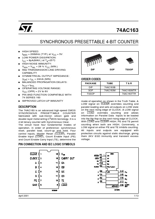
1/13April 2001sHIGH SPEED:f MAX = 200MHz (TYP.) at V CC = 5V sLOW POWER DISSIPATION:I CC = 8µA(MAX.) at T A =25°C sHIGH NOISE IMMUNITY:V NIH = V NIL = 28 % V CC (MIN.)s50Ω TRANSMISSION LINE DRIVING CAPABILITYsSYMMETRICAL OUTPUT IMPEDANCE:|I OH | = I OL = 24mA (MIN)sBALANCED PROPAGATION DELAYS:t PLH ≅ t PHLsOPERATING VOLTAGE RANGE:V CC (OPR) = 2V to 6VsPIN AND FUNCTION COMPATIBLE WITH 74 SERIES 163sIMPROVED LATCH-UP IMMUNITYDESCRIPTIONThe 74AC163 is an advanced high-speed CMOS SYNCRONOUS PRESETTABLE COUNTER fabricated with sub-micron silicon gate and double-layer metal wiring C 2MOS tecnology. It is a 4 bit binary counter with Synchronous Clear.The circuit have four fundamental modes of operation, in order of preference: synchronous reset, parallel load, count-up and hold. Four control inputs, Master Reset (CLEAR), Parallel Enable Input (LOAD), Count Enable Input (PE)and Count Enable Carry Input (TE), determine the mode of operation as shown in the Truth Table. A LOW signal on CLEAR overrides counting and parallel loading and sets all outputs on LOW state on the next rising edge of CLOCK. A LOW signal on LOAD overrides counting and allows information on Parallel Data inputs to be loaded into the flip-flop on the next rising edge of CLOCK.With LOAD and CLEAR HIGH, PE and TE permit counting when both are HIGH. Conversely, a LOW signal on either PE and TE inhibits counting.All inputs and outputs are equipped with protection circuits against static discharge, giving them 2KV ESD immunity and transient excess voltage.74AC163SYNCHRONOUS PRESETTABLE 4-BIT COUNTERPIN CONNECTION AND IEC LOGIC SYMBOLSORDER CODESPACKAGE TUBE T & R DIP 74AC163B SOP 74AC163M74AC163MTR TSSOP74AC163TTR74AC1632/13INPUT AND OUTPUT EQUIVALENT CIRCUIT PIN DESCRIPTIONTRUTH TABLE LOGIC DIAGRAMPIN No SYMBOL NAME AND FUNCTION 1CLEAR Master Reset2CLOCK Clock Input (LOW toHIGH Edge Trigger)3, 4, 5, 6A, B, C, D Data Inputs7PE Count Enable Input10TE Count Enable Carry Input 9LOAD Parallel Enable Input 14, 13, 12,11QA to QD Flip-Flop Outputs 15CARRY OUT Terminal Count Output8GND Ground (0V)16V CC Positive Supply Voltage74AC1633/13TIMING CHART74AC1634/13ABSOLUTE MAXIMUM RATINGSAbsolute Maximum Ratings are those values beyond which damage to the device may occur. Functional operation under these conditions is not implied.RECOMMENDED OPERATING CONDITIONS1) V IN from 30% to 70% of V CCSymbol ParameterValue Unit V CC Supply Voltage -0.5 to +7V V I DC Input Voltage -0.5 to V CC + 0.5V V O DC Output Voltage -0.5 to V CC + 0.5V I IK DC Input Diode Current ± 20mA I OK DC Output Diode Current ± 20mA I O DC Output Current ± 50mA I CC or I GND DC V CC or Ground Current± 300mA T stg Storage Temperature -65 to +150°C T LLead Temperature (10 sec)300°CSymbol ParameterValue Unit V CC Supply Voltage 2 to 6V V I Input Voltage 0 to V CC V V O Output Voltage 0 to V CC V T op Operating Temperature-55 to 125°C dt/dvInput Rise and Fall Time V CC = 3.0, 4.5 or 5.5V (note 1)8ns/V74AC1635/13DC SPECIFICATIONS1) Maximum test duration 2ms, one output loaded at time2) Incident wave switching is guaranteed on transmission lines with impedances as low as 50ΩSymbolParameterTest ConditionValue UnitV CC (V)T A = 25°C -40 to 85°C -55 to 125°C Min.Typ.Max.Min.Max.Min.Max.V IHHigh Level Input Voltage3.0V O = 0.1 V or V CC -0.1V 2.1 1.5 2.1 2.1V4.5 3.15 2.25 3.15 3.155.5 3.852.753.853.85V ILLow Level Input Voltage3.0V O = 0.1 V or V CC -0.1V 1.50.90.90.9V4.5 2.25 1.35 1.35 1.355.5 2.75 1.651.651.65V OHHigh Level Output Voltage3.0I O =-50 µA 2.9 2.99 2.9 2.9V4.5I O =-50 µA 4.4 4.49 4.4 4.45.5I O =-50 µA 5.4 5.495.4 5.43.0I O =-12 mA 2.56 2.46 2.44.5I O =-24 mA 3.86 3.76 3.75.5I O =-24 mA 4.864.764.7V OLLow Level Output Voltage3.0I O =50 µA 0.0020.10.10.1V4.5I O =50 µA 0.0010.10.10.15.5I O =50 µA 0.0010.10.10.13.0I O =12 mA 0.360.440.54.5I O =24 mA 0.360.440.55.5I O =24 mA 0.360.440.5I I Input Leakage Current5.5V I = V CC or GND ± 0.1± 1± 1µA I CC Quiescent Supply Current5.5V I = V CC or GND 880160µA I OLD Dynamic Output Current (note 1, 2)5.5V OLD = 1.65 V max 7550mA I OHDV OHD = 3.85 V min-75-50mA74AC1636/13AC ELECTRICAL CHARACTERISTICS (C L = 50 pF, R L = 500 Ω, Input t r = t f = 3ns)(*) Voltage range is 3.3V ± 0.3V (**) Voltage range is 5.0V ± 0.5VSymbolParameterTest ConditionValueUnitV CC (V)T A = 25°C -40 to 85°C -55 to 125°C Min.Typ.Max.Min.Max.Min.Max.t PLH t PHL Propagation DelayTime CLOCK to Q 3.3(*)7.012.013.013.0ns 5.0(**)5.09.09.59.5t PLH t PHL Propagation DelayTime CLOCK to CARRY OUT3.3(*)8.014.015.015.0ns5.0(**)6.010.511.511.5t PLH t PHL Propagation DelayTime TE to CARRY OUT3.3(*) 5.59.511.011.0ns5.0(**) 4.06.57.57.5t W CK pulse Width,(Count) HIGH or LOW3.3(*) 2.04.57.57.5ns5.0(**)2.0 4.0 4.5 4.5t W CK pulse Width,(Load) HIGH or LOW3.3(*) 2.0 3.0 3.5 3.5ns5.0(**) 2.0 2.5 3.0 3.0t s Setup Time HIGHor LOW (INPUT to CLOCK)3.3(*) 2.04.05.0 5.0ns5.0(**) 1.5 3.0 4.0 4.0t n Hold Time HIGH orLOW (INPUT to CLOCK)3.3(*)-1.5-0.500ns5.0(**)-1.00.5 1.0 1.0t s Setup Time HIGHor LOW (CLEAR to CLOCK)3.3(*) 1.0 3.04.0 4.0ns5.0(**) 1.0 3.5 4.5 4.5t h Hold Time HIGH orLOW (CLEAR to CLOCK)3.3(*)-0.50.5 1.0 1.0ns5.0(**)-0.30.5 1.0 1.0t s Setup Time HIGHor LOW ( LOAD to CLOCK)3.3(*) 3.0 5.08.08.0ns5.0(**) 2.56.07.07.0t h Hold Time HIGH orLOW (LOAD to CLOCK)3.3(*)-2.5-1.0-0.5-0.5ns5.0(**)-1.500.50.5t s Setup Time HIGHor LOW (PE or TE to CLOCK)3.3(*) 3.0 6.07.07.0ns5.0(**) 2.0 4.0 5.0 5.0t h Hold Time HIGH orLOW (PE or TE to CLOCK)3.3(*)-2.0-0.500ns5.0(**)-1.500.50.5f MAX Maximum ClockFrequency3.3(*)702006060MHz5.0(**)110200959574AC1637/13CAPACITIVE CHARACTERISTICSPD load. (Refer to Test Circuit). Average operating current can be obtained by the following equation. I CC(opr) = C PD x V CC x f IN + I CC /n (per circuit)L R L = R 1 = 500Ω or equivalentR T = Z OUT of pulse generator (typically 50Ω)WAVEFORM 1: PROPAGATION DELAYS, COUNT MODE (f=1MHz; 50% duty cycle)SymbolParameterTest ConditionValue UnitV CC (V)T A = 25°C -40 to 85°C -55 to 125°C Min.Typ.Max.Min.Max.Min.Max.C IN Input Capacitance 5.0 4.5pF C PDPower Dissipation Capacitance (note1)5.0f IN = 10MHz37pF74AC1638/13WAVEFORM 2: PROPAGATION DELAYS CLEAR MODE (f=1MHz; 50% duty cycle)WAVEFORM 3: PROPAGATION DELAYS PRESET MODE(f=1MHz; 50% duty cycle)74AC1639/13WAVEFORM 4: PROPAGATION DELAYS COUNTABLE MODE (f=1MHz; 50% duty cycle)WAVEFORM 5: PROPAGATION DELAYS CASCADE MODE(f=1MHz; 50% duty cycle)74AC163 Information furnished is believed to be accurate and reliable. However, STMicroelectronics assumes no responsibility for the consequences of use of such information nor for any infringement of patents or other rights of third parties which may result from its use. No license is granted by implication or otherwise under any patent or patent rights of STMicroelectronics. Specifications mentioned in this publication are subject to change without notice. This publication supersedes and replaces all information previously supplied. STMicroelectronics products are not authorized for use as critical components in life support devices or systems without express written approval of STMicroelectronics.© The ST logo is a registered trademark of STMicroelectronics© 2001 STMicroelectronics - Printed in Italy - All Rights ReservedSTMicroelectronics GROUP OF COMPANIESAustralia - Brazil - China - Finland - France - Germany - Hong Kong - India - Italy - Japan - Malaysia - Malta - MoroccoSingapore - Spain - Sweden - Switzerland - United Kingdom© 13/13。
- 1、下载文档前请自行甄别文档内容的完整性,平台不提供额外的编辑、内容补充、找答案等附加服务。
- 2、"仅部分预览"的文档,不可在线预览部分如存在完整性等问题,可反馈申请退款(可完整预览的文档不适用该条件!)。
- 3、如文档侵犯您的权益,请联系客服反馈,我们会尽快为您处理(人工客服工作时间:9:00-18:30)。
SN54AC533, SN74AC533OCTAL TRANSPARENT DĆTYPE LATCHESWITH 3ĆSTATE OUTPUTSSCAS555C − NOVEMBER 1995 − REVISED OCTOBER 2003
1POST OFFICE BOX 655303 • DALLAS, TEXAS 75265
D2-V to 6-V V
CC Operation
DInputs Accept Voltages to 6 V
DMax t
pd of 10.5 ns at 5 V
D3-State Inverting Outputs Drive Bus Lines
DirectlyDFull Parallel Access for Loading
description/ordering information
The ’AC533 devices are octal transparent D-typelatches with 3-state outputs. When thelatch-enable (LE) input is high, the Q outputsfollow the complements of the data (D) inputs.When LE is taken low, the Q outputs are latchedat the inverse logic levels set up at the D inputs.
A buffered output-enable (OE) input can be usedto place the eight outputs in either a normal logicstate (high or low logic levels) or thehigh-impedance state. In the high-impedancestate, the outputs neither load nor drive the buslines significantly. The high-impedance state andincreased drive provide the capability to drive buslines without need for interface or pullupcomponents.
OE does not affect the internal operations of thelatches. Old data can be retained or new data canbe entered while the outputs are in thehigh-impedance state.
To ensure the high-impedance state during power up or power down, OE should be tied to VCC through a pullupresistor; the minimum value of the resistor is determined by the current-sinking capability of the driver.
ORDERING INFORMATIONTAPACKAGE†ORDERABLEPART NUMBERTOP-SIDEMARKING
PDIP − NTubeSN74AC533NSN74AC533NTubeSN74AC533DWSOIC − DWTape and reelSN74AC533DWRAC533
°°SOP − NSTape and reelSN74AC533NSRAC533−40C to 85CSSOP − DBTape and reelSN74AC533DBRAC533TubeSN74AC533PWTSSOP − PWTape and reelSN74AC533PWRAC533
CDIP − JTubeSNJ54AC533JSNJ54AC533J°°CFP − WTubeSNJ54AC533WSNJ54AC533W−55C to 125CLCCC − FKTubeSNJ54AC533FKSNJ54AC533FK†Package drawings, standard packing quantities, thermal data, symbolization, and PCB design guidelines are
available at www.ti.com/sc/package.
Copyright 2003, Texas Instruments IncorporatedUNLESS OTHERWISE NOTED this document contains PRODUCTION
DATA information current as of publication date. Products conform tospecifications per the terms of Texas Instruments standard warranty.Production processing does not necessarily include testing of allparameters.
Please be aware that an important notice concerning availability, standard warranty, and use in critical applications ofTexasInstruments semiconductor products and disclaimers thereto appears at the end of this data sheet.
1234567891020191817161514131211
OE1Q1D2D2Q3Q3D4D4QGNDVCC
8Q
8D7D7Q6Q6D5D5QLE
SN54AC533...JORWPACKAGESN74AC533...DB, DW, N, NS, OR PW PACKAGE(TOP VIEW)
32120199101112134
5678
1817161514
8D7D7Q6Q6D
2D2Q3Q3D4D
SN54AC533...FK PACKAGE(TOP VIEW)
1D1QOE5Q5D8Q
4QGND
LE
VCC
元器件交易网www.cecb2b.comSN54AC533, SN74AC533OCTAL TRANSPARENT DĆTYPE LATCHESWITH 3ĆSTATE OUTPUTSSCAS555C − NOVEMBER 1995 − REVISED OCTOBER 2003
2POST OFFICE BOX 655303 • DALLAS, TEXAS 75265
FUNCTION TABLE(each latch)
INPUTSOUTPUT
OELEDQ
LHHLLHLHLLXQ0
HXXZ
logic diagram (positive logic)OELE
1D1Q
111
32
To Seven Other ChannelsC1
1D
absolute maximum ratings over operating free-air temperature range (unless otherwise noted)†Supply voltage range, VCC −0.5 V to 7 V. . . . . . . . . . . . . . . . . . . . . . . . . . . . . . . . . . . . . . . . . . . . . . . . . . . . . . . . . . Input voltage range, VI (see Note 1) −0.5 V to VCC + 0.5 V. . . . . . . . . . . . . . . . . . . . . . . . . . . . . . . . . . . . . . . . . . . Output voltage range, VO (see Note 1) −0.5 V to VCC + 0.5 V. . . . . . . . . . . . . . . . . . . . . . . . . . . . . . . . . . . . . . . . Input clamp current, IIK (VI < 0 or VI > VCC) ±20 mA. . . . . . . . . . . . . . . . . . . . . . . . . . . . . . . . . . . . . . . . . . . . . . . .
Output clamp current, IOK (VO < 0 or VO > VCC) ±20 mA. . . . . . . . . . . . . . . . . . . . . . . . . . . . . . . . . . . . . . . . . . . . Continuous output current, IO (VO = 0 to VCC) ±50 mA. . . . . . . . . . . . . . . . . . . . . . . . . . . . . . . . . . . . . . . . . . . . . . Continuous current through VCC or GND ±200 mA. . . . . . . . . . . . . . . . . . . . . . . . . . . . . . . . . . . . . . . . . . . . . . . . . .
Package thermal impedance, θJA (see Note 2):DB package 70°C/W. . . . . . . . . . . . . . . . . . . . . . . . . . . . . . . . . DW package 58°C/W. . . . . . . . . . . . . . . . . . . . . . . . . . . . . . . . . N package 69°C/W. . . . . . . . . . . . . . . . . . . . . . . . . . . . . . . . . . . NS package 60°C/W. . . . . . . . . . . . . . . . . . . . . . . . . . . . . . . . . PW package 83°C/W. . . . . . . . . . . . . . . . . . . . . . . . . . . . . . . . . Storage temperature range, Tstg −65°C to 150°C. . . . . . . . . . . . . . . . . . . . . . . . . . . . . . . . . . . . . . . . . . . . . . . . . . .