AOD4187中文资料
常用稳压管型号
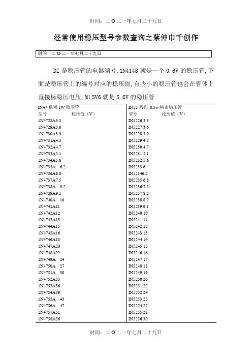
经常使用稳压型号参数查询之蔡仲巾千创作DZ是稳压管的电器编号,1N4148就是一个0.6V的稳压管,下面是稳压管上的编号对应的稳压值,有些小的稳压管也会在管体上直接标稳压电压,如5V6就是5.6V的稳压管.美标稳压二极管型号:HITACHI(日立):HITACHI(日立)0.5W稳压二极管型号参数稳压HZ3A1 2.5~2.7VHZ3A2 2.6~2.8VHZ3A3 2.6~2.9VHZ3B1 2.8~3.0VHZ3B2 2.9~3.1VHZ3B3 3.0~3.2V线性稳压器件(输入输出电流相等,压降3V以上)型号稳压(V) 最年夜输出电流可替代型号79L05 -5V 100mA79L06 -6V 100mA79L08 -8V 100mALM7805 5V 1A L7805,LM340T5LM7806 6V 1A L7806LM7808 8V 1A L7808LM7809 9V 1A L7809LM7812 12V 1A L7812,LM340T12LM7815 15V 1A L7815,LM340T15LM7818 18V 1A L7815LM7824 24V 1A L7824LM7905 -5V 1A L7905LM7906 -6V 1A L7906,KA7906LM7908 -8V 1A L7908LM7909 -9V 1A L7909LM7912 -12V 1A L7912LM7915 -15V 1A L7915LM7918 -18V 1A L7918LM7924 -24V 1A L792478L05 5V 100mA78L06 6V 100mA78L08 8V 100ma78L09 9V 100ma78L12 12V 100ma78L15 15V 100ma78L18 18V 100ma78L24 24V 100ma开关稳压器件(电压转换效率高)型号说明最年夜输出电流LM1575T-3.3 3.3V简易开关电源稳压器1ALM1575T-5.0 5V简易开关电源稳压器1ALM1575T-12 12V简易开关电源稳压器1ALM1575T-15 15V简易开关电源稳压器1ALM1575T-ADJ 简易开关电源稳压器(可调1.23V~37V) 1ALM1575HVT-3.3 3.3V简易开关电源稳压器1ALM1575HVT-5.0 5V简易开关电源稳压器1ALM1575HVT-12 12V简易开关电源稳压器1ALM1575HVT-15 15V简易开关电源稳压器1ALM1575HVT-ADJ 简易开关电源稳压器(可调1.23V~37V) 1ALM2575T-3.3 3.3V简易开关电源稳压器1ALM2575T-5.0 5V简易开关电源稳压器1ALM2575T-12 12V简易开关电源稳压器1ALM2575T-15 15V简易开关电源稳压器1ALM2575T-ADJ 简易开关电源稳压器(可调1.23V~ 37V) 1ALM2575HVT-3.3 3.3V简易开关电源稳压器1ALM2575HVT-5.0 5V简易开关电源稳压器1ALM2575HVT-12 12V简易开关电源稳压器1ALM2575HVT-15 15V简易开关电源稳压器1ALM2575HVT-ADJ 简易开关电源稳压器(可调1.23V~37V) 1ALM2576T-3.3 3.3V简易开关电源稳压器3ALM2576T-5.0 5.0V简易开关电源稳压器3ALM2576T-12 12V简易开关电源稳压器3ALM2576T-15 15V简易开关电源稳压器3ALM2576T-ADJ 简易开关电源稳压器(可调1.23V~37V) 3ALM2576HVT-3.3 3.3V简易开关电源稳压器3ALM2576HVT-5.0 5.0V简易开关电源稳压器3ALM2576HVT-12 12V简易开关电源稳压器3ALM2576HVT-15 15V简易开关电源稳压器3ALM2576HVT-ADJ 简易开关电源稳压器(可调1.23V~37V) 3A。
丹东华奥电子有限公司LD42794汽车半导体说明书
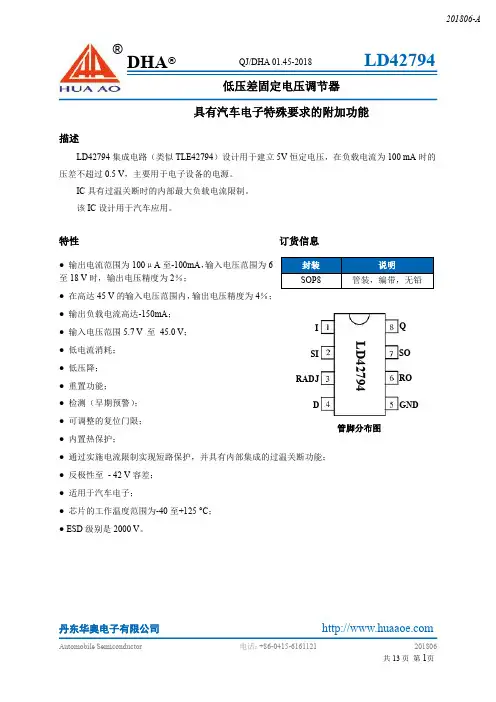
丹东华奥电子有限公司描述LD42794集成电路(类似TLE42794)设计用于建立5V 恒定电压,在负载电流为100mA 时的压差不超过0.5V ,主要用于电子设备的电源。
IC 具有过温关断时的内部最大负载电流限制。
该IC 设计用于汽车应用。
特性订货信息●输出电流范围为100μA 至-100mA ,输入电压范围为6至18V 时,输出电压精度为2%;●在高达45V 的输入电压范围内,输出电压精度为4%;●输出负载电流高达-150mA ;●输入电压范围5.7V 至45.0V ;●低电流消耗;●低压降;●重置功能;●检测(早期预警);●可调整的复位门限;●内置热保护;●通过实施电流限制实现短路保护,并具有内部集成的过温关断功能;●反极性至-42V 容差;●适用于汽车电子;●芯片的工作温度范围为-40至+125°C ;●ESD 级别是2000V 。
封装说明SOP8管装,编带,无铅低压差固定电压调节器具有汽车电子特殊要求的附加功能QSI SO GNDIRO DRADJLD42794管脚分布图表1:管脚描述(SOP8)丹东华奥电子有限公司参考电流和饱和控制整理控制单元参考图1–集成电路方框图注:A1–逻辑元素A2,A3,A5–缓冲区A4–误差放大器G1–复位振荡器R1–R3-电阻VT1–VT4–晶体管丹东华奥电子有限公司丹东华奥电子有限公司注:1缩写:-U D–复位延迟电压(连接管脚4);-C1–电容连接到复位信号延迟输出(连接管脚4);丹东华奥电子有限公司--R1–电阻连接到管脚8。
2表中电流数值前面的符号«-»仅指示其方向(漏极电流)。
*环境温度参考参数:IC温度升高时的关闭温度T j,sd OFF,o C,min./max.=151/200;温度滞后T j,sdh OFF,o C,min./max.=5/30IC工作说明●IC包含:●控制放大器;●参考电压单元;●控制元件;●控制单元;●复位振荡器;●复位门限调节单元;●早期预警单元(检测);●温度感应器;●晶体管电流和饱和控制电路。
SUP57N20-33_08中文资料
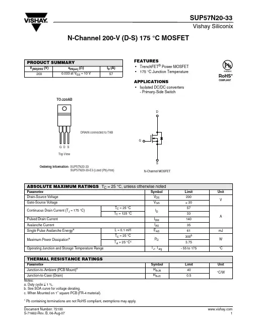
Vishay SiliconixSUP57N20-33N-Channel 200-V (D-S) 175 °C MOSFETFEATURES•TrenchFET ® Power MOSFET •175 °C Junction TemperatureAPPLICATIONS•Isolated DC/DC converters- Primary-Side SwitchPRODUCT SUMMARYV(BR)DSS (V)r DS(on) (Ω)I D (A)2000.033 at V GS = 10 V57Notes:a. Duty cycle ≤ 1 %.b. See SOA curve for voltage derating.c. When Mounted on 1" square PCB (FR-4 material).* Pb containing terminations are not RoHS compliant, exemptions may apply.ABSOLUTE MAXIMUM RATINGS T C = 25°C, unless otherwise notedParameterSymbol Limit Unit Drain-Source Voltage V DS 200VGate-Source VoltageV GS± 20Continuous Drain Current (T J = 175 °C)T C = 25 °C I D 57AT C = 125 °C33Pulsed Drain Current I DM 140Avalanche CurrentI AS35Single Pulse Avalanche Energy a L = 0.1 mH E AS 61mJ Maximum Power DissipationaT C = 25 °C P D 300b W T A = 25 °C c3.75Operating Junction and Storage T emperature RangeT J , T stg- 55 to 175°CTHERMAL RESISTANCE RATINGSParameterSymbol Limit Unit Junction-to-Ambient (PCB Mount)c R thJA 40°C/WJunction-to-Case (Drain)R thJC0.5Vishay SiliconixSUP57N20-33Notes:a. Pulse test; pulse width ≤ 300 µs, duty cycle ≤ 2 %.b. Guaranteed by design, not subject to production testing.c. Independent of operating temperature.Stresses beyond those listed under “Absolute Maximum Ratings” may cause permanent damage to the device. These are stress ratings only, and functional operation of the device at these or any other conditions beyond those indicated in the operational sections of the specifications is not implied. Exposure to absolute maximum rating conditions for extended periods may affect device reliability.SPECIFICATIONS T J = 25°C, unless otherwise notedParameter Symbol Test Conditions Min Typ Max UnitStaticDrain-Source Breakdown Voltage V (BR)DSS V DS = 0 V , I D = 250 µA 200V Gate-Threshold Voltage V GS(th) V DS = V GS , I D = 250 µA 24Gate-Body LeakageI GSS V DS = 0 V, V GS = ± 20 V ± 100nAZero Gate Voltage Drain Current I DSS V DS = 160 V , V GS = 0 V 1µA V DS = 160 V, V GS = 0 V , T J = 125 °C 50V DS = 160 V, V GS = 0 V , T J = 175 °C250On-State Drain Current aI D(on) V DS ≥ 5 V , V GS = 10 V 120A Drain-Source On-State Resistance a r DS(on) V GS = 10 V, I D = 30 A 0.0270.033ΩV GS = 10 V, I D = 30 A, T J = 125 °C 0.069V GS = 10 V, I D = 30 A, T J = 175 °C0.093Forward T ransconductance a g fsV DS = 15 V , I D = 30 A25S Dynamic bInput Capacitance C iss V GS = 0 V , V DS = 25 V , f = 1 MHz5100pFOutput CapacitanceC oss 480Reverse Transfer Capacitance C rss 210Total Gate Charge c Q g V DS = 100 V , V GS = 10 V , ID = 85 A 90130nC Gate-Source Charge c Q gs 23Gate-Drain Charge c Q gd 34Turn-On Delay Time c t d(on) V DD = 100 V, R L = 1.5 Ω I D ≅ 65 A, V GEN = 10 V , R G = 2.5 Ω2435nsRise Time ct r 220330Turn-Off Delay Time c t d(off) 4570Fall Time ct f200300Source-Drain Diode Ratings and Characteristics (T C = 25°C)b Continuous Current I S 65A Pulsed Current I SM 140Forward Voltage a V SD I F = 65 A, V GS = 0 V 1.0 1.5V Reverse Recovery Time t rr I F = 50 A, di/dt = 100 A/µs130200ns Peak Reverse Recovery Current I RM(REC)812A Reverse Recovery ChargeQ rr0.521.2µCOutput CharacteristicsTransfer CharacteristicsVishay SiliconixSUP57N20-33TYPICAL CHARACTERISTICS 25°C, unless otherwise notedAvalanche Current vs. TimeDrain Source Breakdown vs. Junction TemperatureVishay SiliconixSUP57N20-33THERMAL RATINGSVishay Silicon ix main tain s worldwide man ufacturin g capability. Products may be man ufactured at on e of several qualified location s. Reliability data for Silicon Technology and Package Reliability represent a composite of all qualified locations. For related documents such as package/tape drawin gs, part markin g, an d reliability data, see /ppg?72100.Maximum Avalanche and Drain Currentvs. Case TemperatureSafe Operating AreaNormalized Thermal Transient Impedance, Junction-to-CaseDisclaimer Legal Disclaimer NoticeVishayAll product specifications and data are subject to change without notice.Vishay Intertechnology, Inc., its affiliates, agents, and employees, and all persons acting on its or their behalf (collectively, “Vishay”), disclaim any and all liability for any errors, inaccuracies or incompleteness contained herein or in any other disclosure relating to any product.Vishay disclaims any and all liability arising out of the use or application of any product described herein or of any information provided herein to the maximum extent permitted by law. The product specifications do not expand or otherwise modify Vishay’s terms and conditions of purchase, including but not limited to the warranty expressed therein, which apply to these products.No license, express or implied, by estoppel or otherwise, to any intellectual property rights is granted by this document or by any conduct of Vishay.The products shown herein are not designed for use in medical, life-saving, or life-sustaining applications unless otherwise expressly indicated. Customers using or selling Vishay products not expressly indicated for use in such applications do so entirely at their own risk and agree to fully indemnify Vishay for any damages arising or resulting from such use or sale. Please contact authorized Vishay personnel to obtain written terms and conditions regarding products designed for such applications.Product names and markings noted herein may be trademarks of their respective owners.元器件交易网。
OPA4188零漂移4运放
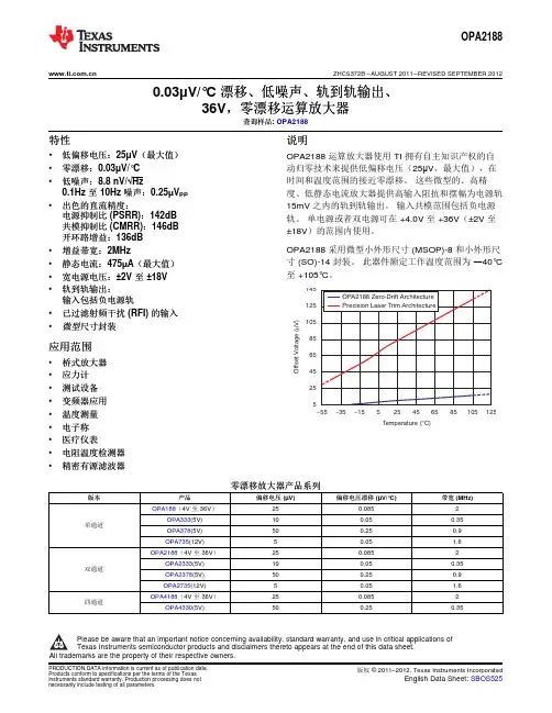
OPA2188 采用微型小外形尺寸 (MSOP)-8 和小外形尺 寸 (SO)-14 封装。 此器件额定工作温度范围为 ―40°C 至 +105°C。
145 OPA2188 Zero-Drift Architecture
125
Precision Laser Trim Architecture
Offset Voltage (mV)
(1) For the most current package and ordering information, see the Package Option Addendum at the end of this document, or visit the device product folder at .
OPA2188
PARAMETER
CONDITIONS
MIN
TYP
OFFSET VOLTAGE
VOS PSRR
Input offset voltage Power-supply rejection ratio Long-term stability
TA = –40°C to +105°C
VS = 4 V to 36 V, VCM = VS / 2
PACKAGE- PACKAGE PRODUCT LEAD DESIGNATOR
OPA2188
SO-8 MSOP-8
D DGK
PACKAGE INFORMATION(1)
SPECIFIED TEMPERATURE
RANGE
PACKAGE MARKING
–40°C to +105°C
2188
–40°C to +105°C
抗硫球阀
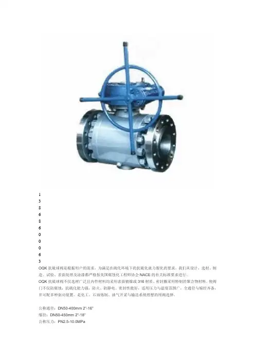
1
3
8
6
8
6
6
3
OQK抗硫球阀是根据用户的需求,为满足在硫化环境下的抗硫化就力裂化的要求,我们从设计,选材、制造、试验、表面处理及涂漆都严格按美国腐蚀化工程师协会NACE的有关标准要求进行。
OQK抗硫球阀不仅选材广泛且内件材料均采用表面镀镍或316材质、密封圈采用特制的聚合物材料。
使阀门不仅防腐蚀,抗硫化能力强,防火、防静电、密封性能好,适用压力与温度范围广,全通径与缩经齐备,并可配多种驱动装置,是化工、石油炼制、油气开采与输送系统理想的用阀选择。
公称通径:DN50-400mm 2"-16"
缩径:DN50-450mm 2"-18"
公称压力:PN2.5-10.0MPa
CLASS:150-900Lb
适用温度:-196℃-300℃主要性能及规范
型号、零件材料及主要参数。
AOD438中文资料
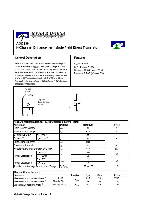
SymbolTyp Max 14.2203950R θJC 0.8 1.5Maximum Junction-to-AmbientASteady-State °C/W Maximum Junction-to-CaseCSteady-State°C/WThermal Characteristics ParameterUnits Maximum Junction-to-Ambient At ≤ 10s R θJA °C/W AOD438AOD438SymbolMin TypMaxUnits BV DSS 30V 1T J =55°C5I GSS 100nA V GS(th)1 1.83V I D(ON)85A 2.8 3.5T J =125°C4.45.54.4 5.5m Ωg FS 106S V SD 0.721V I S85A C iss 32003840pF C oss 590pF C rss 414pF R g0.540.7ΩQ g (10V)6376nC Q g (4.5V)3340nC Q gs 8.6nC Q gd 17.6nC t D(on)12ns t r 15.5ns t D(off)40ns t f 14ns t rr 3441ns Q rr30nCTHIS PRODUCT HAS BEEN DESIGNED AND QUALIFIED FOR THE CONSUMER MARKET. APPLICATIONS OR USES AS CRITICAL COMPONENTS IN LIFE SUPPORT DEVICES OR SYSTEMS ARE NOT AUTHORIZED. AOS DOES NOT ASSUME ANY LIABILITY ARISING OUT OF SUCH APPLICATIONS OR USES OF ITS PRODUCTS. AOS RESERVES THE RIGHT TO IMPROVE PRODUCT DESIGN,FUNCTIONS AND RELIABILITY WITHOUT NOTICE.Gate Drain Charge V GS =0V, V DS =15V, f=1MHz SWITCHING PARAMETERS Total Gate Charge Gate Source Charge Gate resistanceV GS =0V, V DS =0V, f=1MHzV GS =4.5V, V DS =15V, I D =20ATotal Gate Charge Turn-On Rise Time Turn-Off DelayTime V GS =10V, V DS =15V, R L =0.75Ω, R GEN =3ΩTurn-Off Fall TimeTurn-On DelayTime m ΩV GS =4.5V, I D =20AI S =1A,V GS =0VV DS =5V, I D =20AMaximum Body-Diode Continuous CurrentInput Capacitance Output CapacitanceDYNAMIC PARAMETERS R DS(ON)Static Drain-Source On-ResistanceForward TransconductanceDiode Forward Voltage I DSS µA Gate Threshold Voltage V DS =V GS I D =250µA V DS =24V, V GS =0VV DS =0V, V GS = ±20V Zero Gate Voltage Drain Current Gate-Body leakage current Electrical Characteristics (T J =25°C unless otherwise noted)STATIC PARAMETERS Parameter Conditions Body Diode Reverse Recovery TimeBody Diode Reverse Recovery Charge I F =20A, dI/dt=100A/µsDrain-Source Breakdown Voltage On state drain currentI D =250µA, V GS =0V V GS =10V, V DS =5V V GS =10V, I D =20AReverse Transfer Capacitance I F =20A, dI/dt=100A/µsA: The value of R θJA is measured with the device mounted on 1in 2 FR-4 board with 2oz. Copper, in a still air environment with T A =25°C. The Power dissipation P DSM is based on steady-state R θJA and the maximum allowed junction temperature of 150°C. The value in any givenapplication depends on the user's specific board design, and the maximum temperature of 175°C may be used if the PCB or heatsink allows it.B. The power dissipation P D is based on T J(MAX)=175°C, using junction-to-case thermal resistance, and is more useful in setting the upperdissipation limit for cases where additional heatsinking is used. It is used to determine the current rating, when this rating falls below the package limit.C: Repetitive rating, pulse width limited by junction temperature T J(MAX)=175°C.D. The R θJA is the sum of the thermal impedence from junction to case R θJC and case to ambient.E. The static characteristics in Figures 1 to 6 are obtained using <300 µs pulses, duty cycle 0.5% max.F. These tests are performed with the device mounted on 1 in 2 FR-4 board with 2oz. Copper, in a still air environment with T A =25°C. The SOA curve provides a single pulse rating.G. The maximum current rating is limited by the package current capability. Rev 2: July 2005AOD438AOD438AOD438。
ADA4817-1中文资料
FEATURES
High speed −3 dB bandwidth (G = 1, RL = 100 Ω): 1050 MHz Slew rate: 870 V/μs 0.1% settling time: 9 ns
Low input bias current: 2 pA Low input capacitance
NC = NO CONNECT
Figure 1. 8-Lead ADA4817-1 LFCSP (CP-8-2)
ADA4817-2
TOP VIEW (Not to Scale)
16 FB1 15 PD1 14 +VS1 13 OUT1
–IN1 1 +IN1 2
NC 3 –VS2 4
12 –VS1 11 NC 10 +IN2 9 –IN2
Low Noise, 1 GHz FastFET Op Amps ADA4817-1/ADA4817-2
CONNECTION DIAGRAMS
ADA4817-1
TOP VIEW (Not to Scale)
PD 1 FB 2 –T 6 NC 5 –VS
07756-001
元器件交易网
ADA4817-1/ADA4817-2
TABLE OF CONTENTS
Features .............................................................................................. 1 Applications....................................................................................... 1 Connection Diagrams...................................................................... 1 General Description ......................................................................... 1 Revision History ............................................................................... 2 Specifications..................................................................................... 3
AOD冶炼设备主要参数一缆表
~5620
托圈高度
mm
1408
托圈外径
mm
4858
托圈内径
mm
4258
负载容量
ton
200
托圈的耳轴直径
mm
~530
轴承座
PCS
2
倾炉驱动机构
AOD炉倾动速度
rpm
0.2-1.0
总传动比
1168.42
电动机
KW
18.5×4
力矩能力
KN.M
~500
定位系统
绝对值编码器
顶枪
顶枪长度
mm
~5700
顶枪直径
mm
~150
氧气流量
Nm3/min
最大80
氧气压力(顶枪入口)
Mpa
~1.1
冷却水流量
m3/h
~50
冷却水压力(顶枪入口)
Mpa
~1.2
喷吹对冷却水入口/出口平均升温
0C
<15
70TAOD炉
炉子跨二期
3台
AOD炉体
公称容量
t
70
炉体直径
mm
4644
炉体高度
mm
6160(有效高度)
新砌筑耐材的炉体容积比
型号
两台ZSSP-9000
总容量
千伏安
18000
一次电压
千伏
35
二次电压
伏
1000
中频电源
功率范围
千瓦
10000~16000
进线电压
伏
1000
最大进线电流
安
260600
中频频率
赫兹
150
设备名称
设备安装位置
AOD4184中文资料
SymbolTyp Max 18224455R θJC2.43Steady-StateMaximum Junction-to-AmbientA,GSteady-State °C/WThermal Characteristics ParameterUnits Maximum Junction-to-AmbientA,Gt ≤ 10s R θJA °C/W °C/W Maximum Junction-to-CaseD,FAOD4184SymbolMin TypMaxUnits BV DSS 40V 1T J =55°C5I GSS ±100nA V GS(th) 1.7 2.23V I D(ON)120A6.78T J =125°C11138.511g FS 100S V SD 0.721V I S20A C iss 1500pF C oss 215pF C rss 135pF R g23.55ΩQ g (10V)27.235.4nC Q g (4.5V)13.6nC Q gs 4.5nC Q gd 6.4nC t D(on) 6.4ns t r 17.2ns t D(off)29.6ns t f 16.8ns t rr 2938ns Q rr26nC COMPONENTS IN LIFE SUPPORT DEVICES OR SYSTEMS ARE NOT AUTHORIZED. AOS DOES NOT ASSUME ANY LIABILITY ARISING OUT OF SUCH APPLICATIONS OR USES OF ITS PRODUCTS. AOS RESERVES THE RIGHT TO IMPROVE PRODUCT DESIGN,FUNCTIONS AND RELIABILITY WITHOUT NOTICE.TBDGate Source Charge Gate resistanceV GS =0V, V DS =0V, f=1MHzV GS =10V, V DS =20V, I D =20ATBD Total Gate Charge m ΩTurn-On Rise Time Turn-Off DelayTime V GS =10V, V DS =20V, R L =1Ω, R GEN =3ΩTurn-Off Fall TimeTurn-On DelayTime Gate Drain Charge V GS =0V, V DS =20V, f=1MHz SWITCHING PARAMETERS Total Gate Charge V GS =4.5V, I D =15AI S =1A,V GS =0V V DS =5V, I D =20AMaximum Body-Diode Continuous CurrentInput Capacitance Output Capacitance DYNAMIC PARAMETERS R DS(ON)Static Drain-Source On-ResistanceForward TransconductanceDiode Forward VoltageElectrical Characteristics (T J =25°C unless otherwise noted)STATIC PARAMETERS ParameterConditions I DSS µA Body Diode Reverse Recovery ChargeI F =20A, dI/dt=100A/µsBody Diode Reverse Recovery Time V GS =10V, I D =20AReverse Transfer Capacitance I F =20A, dI/dt=100A/µs Gate Threshold Voltage V DS =V GS I D =250µA Drain-Source Breakdown Voltage On state drain currentI D =250µA, V GS =0V V GS =10V, V DS =5V V DS =40V, V GS =0VV DS =0V, V GS = ±20V Zero Gate Voltage Drain Current Gate-Body leakage current A: The value of R θJA is measured with the device in a still air environment with T A =25°C. The power dissipation P DSM and current rating I DSM are based on T J(MAX)=150°C, using steady state junction-to-ambient thermal resistance.B. The power dissipation P D is based on T J(MAX)=175°C, using junction-to-case thermal resistance, and is more useful in setting the upper dissipation limit for cases where additional heatsinking is used.C: Repetitive rating, pulse width limited by junction temperature T J(MAX)=175°C.D. The R θJA is the sum of the thermal impedence from junction to case R θJC and case to ambient.E. The static characteristics in Figures 1 to 6 are obtained using <300 µs pulses, duty cycle 0.5% max.F. These curves are based on the junction-to-case thermal impedence which is measured with the device mounted to a large heatsink, assuming a maximum junction temperature of T J(MAX)=175°C. The SOA curve provides a single pulse rating.G. These tests are performed with the device mounted on 1 in 2 FR-4 board with 2oz. Copper, in a still air environment with T A =25°C.H. The maximum current rating is limited by bond-wires. Rev0: March 2008。
AOD4144中文资料
ID=250µA, VGS=0V
30
V
IDSS
Zero Gate Voltage Drain Current
VDS=30V, VGS=0V
TJ=55°C
10 µA
50
IGSS
Gate-Body leakage current
VDS=0V, VGS= ±20V
100 nA
VGS(th) Gate Threshold Voltage
VDS (V) =30V ID = 55A RDS(ON) < 8mΩ RDS(ON) < 14mΩ
(VGS = 10V) (VGS = 10V) (VGS = 4.5V)
- RoHS Compliant - Halogen Free
100% UIS Tested! 100% R g Tested!
RθJA
18 44
22 55
Maximum Junction-to-Case
Steady-State
RθJC
2.4
3
Alpha & Omega Semiconductor, Ltd.
Units V V
A
A A mJ W
W °C
Units °C/W °C/W °C/W
元器件交易网
4.5V
50
40
4V
30
20
10
VGS=3.5V
0
0
1
2
3
4
5
VDS (Volts) Fig 1: On-Region Characteristics (Note E)
ID(A)
100
VDS=5V 80
60
- 1、下载文档前请自行甄别文档内容的完整性,平台不提供额外的编辑、内容补充、找答案等附加服务。
- 2、"仅部分预览"的文档,不可在线预览部分如存在完整性等问题,可反馈申请退款(可完整预览的文档不适用该条件!)。
- 3、如文档侵犯您的权益,请联系客服反馈,我们会尽快为您处理(人工客服工作时间:9:00-18:30)。
Symbol V DS V GSI DMI AR E AR SymbolTyp Max 15204150R θJC2 2.5T =70°CContinuous Drain T C =25°C I DSM T C =100°CP D T C =100°C I D Continuous Drain Parameter T C =25°C T C =100°C Maximum Junction-to-Ambient A D Steady-State Avalanche CurrentCPower DissipationAT A =25°C P DSM °C/W Absolute Maximum Ratings T A =25°C unless otherwise noted Pulsed Drain Current CPower DissipationBT C =25°C Gate-Source Voltage Drain-Source Voltage Maximum Junction-to-CaseSteady-State°C/WThermal CharacteristicsParameterUnits Maximum Junction-to-Ambient A t ≤ 10s R θJA °C/W Repetitive avalanche energy L=0.1mH CAOD4187P-Channel Enhancement Mode Field Effect Transistor= -10V) = -10V) = -4.5V) 100% UIS Tested! 100% Rg Tested!General DescriptionThe AOD4187 uses advanced trench technology and DSGD-PAKTop ViewSBottom ViewDGSSymbolMin TypMaxUnits BV DSS -40V -1T J =55°C -5I GSS ±100nA V GS(th)-1.7-1.9-3V I D(ON)-100A1417T J =125°C 21261823g FS 40S V SD -0.7-1V I S-50A C iss 196023502850pF C oss 185240320pF C rss 130185260pF R g2 5.511ΩQ g (-10V)354250nC Q g (-4.5V)162025nC Q gs 5.5 6.68nC Q gd 79.714nC t D(on)9.6ns t r 29ns t D(off)56ns t f 19.2ns t rr 141721ns Q rr404960nC COMPONENTS IN LIFE SUPPORT DEVICES OR SYSTEMS ARE NOT AUTHORIZED. AOS DOES NOT ASSUME ANY LIABILITY ARISING OUT OF SUCH APPLICATIONS OR USES OF ITS PRODUCTS. AOS RESERVES THE RIGHT TO IMPROVE PRODUCT DESIGN,FUNCTIONS AND RELIABILITY WITHOUT NOTICEBody Diode Reverse Recovery TimeBody Diode Reverse Recovery Charge I F =-12A, dI/dt=500A/µsDrain-Source Breakdown Voltage On state drain currentI D =-250µA, V GS =0V V GS =-10V, V DS =-5V V GS =-10V, I D =-12AReverse Transfer Capacitance I F =-12A, dI/dt=500A/µsElectrical Characteristics (T J =25°C unless otherwise noted)STATIC PARAMETERS ParameterConditions I DSS µA Gate Threshold Voltage V DS =V GS I D =-250µA V DS =-40V, V GS =0VV DS =0V, V GS = ±20V Zero Gate Voltage Drain Current Gate-Body leakage current Forward Transconductance Diode Forward VoltageR DS(ON)Static Drain-Source On-ResistanceMaximum Body-Diode Continuous CurrentInput Capacitance Output CapacitanceDYNAMIC PARAMETERS I S =-1A,V GS =0VV DS =-5V, I D =-12A V GS =-4.5V, I D =-8Am ΩTurn-On Rise Time Turn-Off DelayTime V GS =-10V, V DS =-20V, R L =1.6Ω,R GEN =3ΩTurn-Off Fall TimeTurn-On DelayTime Total Gate Charge Gate Drain Charge V GS =0V, V DS =-20V, f=1MHz SWITCHING PARAMETERS Gate Source Charge Gate resistanceV GS =0V, V DS =0V, f=1MHzTotal Gate Charge V GS =-10V, V DS =-20V, I D =-12AA: The value of R θJA is measured with the device mounted on 1in 2 FR-4 board with 2oz. Copper, in a still air environment with T A =25°C. The Power dissipation P DSM is based on R θJA and the maximum allowed junction temperature of 150°C. The value in any given application depends on the user's specific board design, and the maximum temperature of 175°C may be used if the PCB allows i t.B. The power dissipation P D is based on T J(MAX)=175°C, using junction-to-case thermal resistance, and is more useful in setting the upper dissipation limit for cases where additional heatsinking is used.C: Repetitive rating, pulse width limited by junction temperature T J(MAX)=175°C. Ratings are based on low frequency and duty cycles to keepinitial T J =25°C.D. The R θJA is the sum of the thermal impedence from junction to case R θJC and case to ambient.E. The static characteristics in Figures 1 to 6 are obtained using <300µs pulses, duty cycle 0.5% max.F. These curves are based on the junction-to-case thermal impedence which is measured with the device mounted to a large heatsink, assuming a maximum junction temperature of T J(MAX)=175°C.The SOA curve provides a single pulse rating.G. The maximum current rating is limited by bond-wires.H. These tests are performed with the device mounted on 1 in 2 FR-4 board with 2oz. Copper, in a still air environment with T A =25°C.*This device is guaranteed green after data code 8X11 (Sep 1ST 2008). Rev 1: Oct-2008VdsChargeGate Charge Test Circuit & WaveformVddVdsIdVgsUnclamped Inductive Switching (UIS) Test Circuit & Waveforms2E = 1/2 LI AR ARBV DSSI ARVdd VddResistive Switching Test Circuit & Waveforms。