MA4L032-31中文资料
ATTINY28L-4PC,ATTINY28L-4PI,ATTINY28L-4AC,ATTINY28L-4AU,ATTINY28L-4AI,规格书,Datasheet 资料
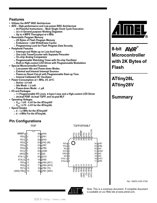
1Features•Utilizes the AVR ® RISC Architecture•AVR – High-performance and Low-power RISC Architecture–90 Powerful Instructions – Most Single Clock Cycle Execution –32 x 8 General-purpose Working Registers –Up to 4 MIPS Throughput at 4 MHz •Nonvolatile Program Memory–2K Bytes of Flash Program Memory –Endurance: 1,000 Write/Erase Cycles–Programming Lock for Flash Program Data Security •Peripheral Features–Interrupt and Wake-up on Low-level Input–One 8-bit Timer/Counter with Separate Prescaler –On-chip Analog Comparator–Programmable Watchdog Timer with On-chip Oscillator–Built-in High-current LED Driver with Programmable Modulation •Special Microcontroller Features–Low-power Idle and Power-down Modes –External and Internal Interrupt Sources–Power-on Reset Circuit with Programmable Start-up Time –Internal Calibrated RC Oscillator •Power Consumption at 1 MHz, 2V , 25°C –Active: 3.0 mA –Idle Mode: 1.2 mA–Power-down Mode: <1 µA •I/O and Packages–11 Programmable I/O Lines, 8 Input Lines and a High-current LED Driver –28-lead PDIP , 32-lead TQFP , and 32-pad MLF •Operating Voltages–V CC : 1.8V - 5.5V for the ATtiny28V –V CC : 2.7V - 5.5V for the ATtiny28L •Speed Grades–0 - 1.2 MHz for the ATtiny28V –0 - 4 MHz For the ATtiny28LPin ConfigurationsPDIPTQFP/QFN/MLF8-bit Microcontroller with 2K Bytes of ATtiny28L ATtiny28V SummaryNote: This is a summary document. A complete documentis available on our Web site at .2ATtiny28L/V1062FS–AVR–07/06DescriptionThe ATtiny28 is a low-power CMOS 8-bit microcontroller based on the AVR RISC archi-tecture. By executing powerful instructions in a single clock cycle, the ATtiny28 achieves throughputs approaching 1 MIPS per MHz, allowing the system designer to optimize power consumption versus processing speed. The AVR core combines a rich instruction set with 32 general-purpose working registers. All the 32 registers are directly con-nected to the Arithmetic Logic Unit (ALU), allowing two independent registers to be accessed in one single instruction executed in one clock cycle. The resulting architec-ture is more code efficient while achieving throughputs up to ten times faster than conventional CISC microcontrollers.Block DiagramFigure 1. The ATtiny28 Block DiagramThe ATtiny28 provides the following features: 2K bytes of Flash, 11 general-purpose I/O lines, 8 input lines, a high-current LED driver, 32 general-purpose working registers, an 8-bit timer/counter, internal and external interrupts, programmable Watchdog Timer with internal oscillator and 2 software-selectable power-saving modes. The Idle Mode stops the CPU while allowing the timer/counter and interrupt system to continue functioning.The Power-down mode saves the register contents but freezes the oscillator, disabling all other chip functions until the next interrupt or hardware reset. The wake-up or inter-3ATtiny28L/V1062FS–AVR–07/06rupt on low-level input feature enables the ATtiny28 to be highly responsive to external events, still featuring the lowest power consumption while in the power-down modes.The device is manufactured using Atmel’s high-density, nonvolatile memory technology.By combining an enhanced RISC 8-bit CPU with Flash on a monolithic chip, the Atmel ATtiny28 is a powerful microcontroller that provides a highly flexible and cost-effective solution to many embedded control applications. The ATtiny28 AVR is supported with a full suite of program and system development tools including: macro assemblers, pro-gram debugger/simulators, in-circuit emulators and evaluation kits.Pin DescriptionsVCC Supply voltage pin.GNDGround pin.Port A (PA3..PA0)Port A is a 4-bit I/O port. PA2 is output-only and can be used as a high-current LED driver. At V CC = 2.0V, the PA2 output buffer can sink 25 mA. PA3, PA1 and PA0 are bi-directional I/O pins with internal pull-ups (selected for each bit). The port pins are tri-stated when a reset condition becomes active, even if the clock is not running.Port B (PB7..PB0)Port B is an 8-bit input port with internal pull-ups (selected for all Port B pins). Port B pins that are externally pulled low will source current if the pull-ups are activated.Port B also serves the functions of various special features of the ATtiny28 as listed on page 27. If any of the special features are enabled, the pull-up(s) on the corresponding pin(s) is automatically disabled. The port pins are tri-stated when a reset condition becomes active, even if the clock is not running.Port D (PD7..PD0)Port D is an 8-bit I/O port. Port pins can provide internal pull-up resistors (selected for each bit). The port pins are tri-stated when a reset condition becomes active, even if the clock is not running.XTAL1Input to the inverting oscillator amplifier and input to the internal clock operating circuit.XTAL2Output from the inverting oscillator amplifier.pulses longer than 50 ns will generate a reset, even if the clock is not running. Shorter pulses are not guaranteed to generate a reset.4ATtiny28L/V1062FS–AVR–07/06Notes:1.For compatibility with future devices, reserved bits should be written to zero if accessed. Reserved I/O memory addressesshould never be written.2.Some of the status flags are cleared by writing a logical “1” to them. Note that the CBI and SBI instructions will operate on allbits in the I/O register, writing a one back into any flag read as set, thus clearing the flag. The CBI and SBI instructions work with registers $00 to $1F only.Register SummaryAddressNameBit 7Bit 6Bit 5Bit 4Bit 3Bit 2Bit 1Bit 0Page$3F SREG ITHSVNZCpage 6$3E Reserved ...Reserved $20Reserved $1F Reserved $1E Reserved $1D Reserved $1C Reserved $1B PORTA ----PORTA3PORTA2PORTA1PORTA0page 32$1A PACR ----DDA3PA2HCDDA1DDA0page 32$19PINA ----PINA3-PINA1PINA0page 32$18Reserved $17Reserved $16PINB PINB7PINB6PINB5PINB4PINB3PINB2PINB1PINB0page 32$15Reserved $14Reserved $13Reserved $12PORTD PORTD7PORTD6PORTD5PORTD4PORTD3PORTD2PORTD1PORTD0page 33$11DDRD DDD7DDD6DDD5DDD4DDD3DDD2DDD1DDD0page 33$10PIND PIND7PIND6PIND5PIND4PIND3PIND2PIND1PIND0page 33$0F Reserved $0E Reserved $0D Reserved $0C Reserved $0B Reserved $0A Reserved $09Reserved $08ACSR ACD -ACO ACI ACIE -ACIS1ACIS0page 44$07MCUCS PLUPB -SE SM WDRF -EXTRF PORF page 19$06ICR INT1INT0LLIE TOIE0ISC11ISC10ISC01ISC00page 22$05IFR INTF1INTF0-TOV0----page 23$04TCCR0FOV0--OOM01OOM00CS02CS01CS00page 35$03TCNT0Timer/Counter0 (8-bit)page 36$02MODCR ONTIM4ONTIM3ONTIM2ONTIM1 ONTIM0MCONF2MCONF1MCONF0page 43$01WDTCR ---WDTOEWDEWDP2WDP1WDP0page 37$00OSCCALOscillator Calibration Registerpage 95ATtiny28L/V1062FS–AVR–07/06Instruction Set SummaryMnemonicOperandsDescriptionOperationFlags# ClocksARITHMETIC AND LOGIC INSTRUCTIONSADD Rd, Rr Add Two RegistersRd ← Rd + Rr Z,C,N,V,H 1ADC Rd, Rr Add with Carry Two Registers Rd ← Rd + Rr + C Z,C,N,V,H 1SUB Rd, Rr Subtract Two Registers Rd ← Rd - Rr Z,C,N,V,H 1SUBI Rd, K Subtract Constant from Register Rd ← Rd - K Z,C,N,V,H 1SBC Rd, Rr Subtract with Carry Two Registers Rd ← Rd - Rr - C Z,C,N,V,H 1SBCI Rd, K Subtract with Carry Constant from Reg.Rd ← Rd - K - C Z,C,N,V,H 1AND Rd, Rr Logical AND RegistersRd ← Rd • Rr Z,N,V 1ANDI Rd, K Logical AND Register and Constant Rd ← Rd • K Z,N,V 1OR Rd, Rr Logical OR RegistersRd ← Rd v Rr Z,N,V 1ORI Rd, K Logical OR Register and Constant Rd ← Rd v K Z,N,V 1EOR Rd, Rr Exclusive OR Registers Rd ← Rd ⊕ Rr Z,N,V 1COM Rd One’s Complement Rd ← $FF - Rd Z,C,N,V 1NEG Rd Two’s Complement Rd ← $00 - Rd Z,C,N,V,H 1SBR Rd, K Set Bit(s) in Register Rd ← Rd v K Z,N,V 1CBR Rd, K Clear Bit(s) in Register Rd ← Rd • (FFh - K)Z,N,V 1INC Rd Increment Rd ← Rd + 1Z,N,V 1DEC Rd DecrementRd ← Rd - 1 Z,N,V 1TST Rd Test for Zero or Minus Rd ← Rd • Rd Z,N,V1CLR Rd Clear Register Rd ← Rd ⊕ Rd Z,N,V 1SER Rd Set Register Rd ← $FF None 1BRANCH INSTRUCTIONSRJMP k Relative JumpPC ← PC + k + 1None 2RCALL kRelative Subroutine Call PC ← PC + k + 1None 3RET Subroutine Return PC ← STACK None 4RETI Interrupt Return PC ← STACKI 4CPSE Rd, Rr Compare, Skip if Equal if (Rd = Rr) PC ← PC + 2 or 3None 1/2CP Rd, Rr CompareRd - Rr Z,N,V,C,H 1CPC Rd, Rr Compare with CarryRd - Rr - C Z,N,V,C,H 1CPI Rd, K Compare Register with Immediate Rd - KZ N,V,C,H 1SBRC Rr, b Skip if Bit in Register Cleared if (Rr(b) = 0) PC ← PC + 2 or 3None 1/2SBRS Rr, b Skip if Bit in Register is Set if (Rr(b) = 1) PC ← PC + 2 or 3None 1/2SBIC P, b Skip if Bit in I/O Register Cleared if (P(b) = 0) PC ← PC + 2 or 3None 1/2SBIS P, b Skip if Bit in I/O Register is Set if (P(b) = 1) PC ← PC + 2 or 3None 1/2BRBS s, k Branch if Status Flag Set if (SREG(s) = 1) then PC ← PC + k + 1None 1/2BRBC s, k Branch if Status Flag Cleared if (SREG(s) = 0) then PC ← PC + k + 1None 1/2BREQ k Branch if Equal if (Z = 1) then PC ← PC + k + 1None 1/2BRNE k Branch if Not Equal if (Z = 0) then PC ← PC + k + 1None 1/2BRCS k Branch if Carry Set if (C = 1) then PC ← PC + k + 1None 1/2BRCC k Branch if Carry Cleared if (C = 0) then PC ← PC + k + 1None 1/2BRSH k Branch if Same or Higher if (C = 0) then PC ← PC + k + 1None 1/2BRLO k Branch if Lower if (C = 1) then PC ← PC + k + 1None 1/2BRMI k Branch if Minus if (N = 1) then PC ← PC + k + 1None 1/2BRPL k Branch if Plusif (N = 0) then PC ← PC + k + 1None 1/2BRGE k Branch if Greater or Equal, Signed if (N ⊕ V = 0) then PC ← PC + k + 1None 1/2BRLT k Branch if Less than Zero, Signed if (N ⊕ V = 1) then PC ← PC + k + 1None 1/2BRHS k Branch if Half-carry Flag Set if (H = 1) then PC ← PC + k + 1None 1/2BRHC k Branch if Half-carry Flag Cleared if (H = 0) then PC ← PC + k + 1None 1/2BRTS k Branch if T-flag Set if (T = 1) then PC ← PC + k + 1None 1/2BRTC k Branch if T-flag Cleared if (T = 0) then PC ← PC + k + 1None 1/2BRVS k Branch if Overflow Flag is Set if (V = 1) then PC ← PC + k + 1None 1/2BRVC k Branch if Overflow Flag is Cleared if (V = 0) then PC ← PC + k + 1None 1/2BRIE k Branch if Interrupt Enabled if (I = 1) then PC ← PC + k + 1None 1/2BRIDkBranch if Interrupt Disabledif (I = 0) then PC ← PC + k + 1None1/26ATtiny28L/V1062FS–AVR–07/06DATA TRANSFER INSTRUCTIONSLD Rd, Z Load Register Indirect Rd ← (Z)None 2ST Z, Rr Store Register Indirect (Z) ← Rr None 2MOV Rd, Rr Move between Registers Rd ← Rr None 1LDI Rd, K Load Immediate Rd ←K None 1IN Rd, P In Port Rd ← P None 1OUT P, RrOut PortP ← Rr None 1LPMLoad Program MemoryR0 ← (Z)None3BIT AND BIT-TEST INSTRUCTIONS SBI P, b Set Bit in I/O Register I/O(P,b) ← 1None 2CBI P, b Clear Bit in I/O Register I/O(P,b) ←None 2LSL Rd Logical Shift LeftRd(n+1) ← Rd(n), Rd(0) ← 0Z,C,N,V 1LSR Rd Logical Shift Right Rd(n) ← Rd(n+1), Rd(7) ← 0Z,C,N,V 1ROL Rd Rotate Left through Carry Rd(0) ← C, Rd(n+1) ← Rd(n), C ← Rd(7)Z,C,N,V 1ROR Rd Rotate Right through Carry Rd(7) ← C, Rd(n) ← Rd(n+1), C ← Rd(0)Z,C,N,V 1ASR Rd Arithmetic Shift Right Rd(n) ← Rd(n+1), n = 0..6Z,C,N,V 1SWAP Rd Swap Nibbles Rd(3..0) ← Rd(7..4), Rd(7..4) ← Rd(3..0)None 1BSET s Flag Set SREG(s) ← 1SREG(s)1BCLR s Flag Clear SREG(s) ← 0SREG(s)1BST Rr, b Bit Store from Register to T T ← Rr(b)T 1BLD Rd, bBit Load from T to Register Rd(b) ← T None 1SEC Set Carry C ← 1C 1CLC Clear Carry C ←0C 1SEN Set Negative Flag N ← 1N 1CLN Clear Negative Flag N ← 0N 1SEZ Set Zero Flag Z ←1Z 1CLZ Clear Zero Flag Z ← 0Z1SEI Global Interrupt Enable I ← 1I 1CLI Global Interrupt Disable I ←I 1SES Set Signed Test FlagS ← 1S 1CLS Clear Signed Test Flag S ←0S 1SEV Set Two’s Complement OverflowV ←1V 1CLV Clear Two’s Complement Overflow V ← 0V 1SET Set T in SREG T ← 1T 1CLT Clear T in SREG T ← 0T 1SEH Set Half-carry Flag in SREG H ← 1H 1CLH Clear Half-carry Flag in SREG H ←H 1NOP No Operation None 1SLEEP Sleep(see specific descr. for Sleep function)None 1WDRWatchdog Reset(see specific descr. for WDR/timer)None1Instruction Set Summary (Continued)MnemonicOperandsDescriptionOperationFlags# Clocks7ATtiny28L/V1062FS–AVR–07/06Notes:1.This device can also be supplied in wafer form. Please contact your local Atmel sales office for detailed ordering informationand minimum quantities.2.Pb-free packaging alternative, complies to the European Directive for Restriction of Hazardous Substances (RoHS direc-tive).Also Halide free and fully Green.Ordering InformationSpeed (MHz)Power Supply (Volts)Ordering Code Package (1)Operation Range 42.7 - 5.5A Ttiny28L-4AC A Ttiny28L-4PC A Ttiny28L-4MC32A 28P332M1-A Commercial (0°C to 70°C)A Ttiny28L-4AI A Ttiny28L-4AU (2)A Ttiny28L-4PI A Ttiny28L-4PU (2)A Ttiny28L-4MI A Ttiny28L-4MU (2)32A 32A 28P328P332M1-A 32M1-A Industrial (-40°C to 85°C)1.21.8 - 5.5A Ttiny28V-1AC A Ttiny28V-1PC A Ttiny28V-1MC32A 28P332M1-A Commercial (0°C to 70°C)A Ttiny28V-1AI A Ttiny28V-1AU (2)A Ttiny28V-1PI A Ttiny28V-1PU (2)A Ttiny28V-1MI A Ttiny28V-1MU (2)32A 32A 28P328P332M1-A 32M1-AIndustrial (-40°C to 85°C)Package Type32A 32-lead, Thin (1.0 mm) Plastic Quad Flat Package (TQFP)28P328-lead, 0.300" Wide, Plastic Dual Inline Package (PDIP)32M1-A32-pad, 5x5x1.0 body, Lead Pitch 0.50mm, Quad Flat No-lead/Micro Lead Frame Package (QFN/MLF)8ATtiny28L/V1062FS–AVR–07/06Packaging Information32A9ATtiny28L/V1062FS–AVR–07/0628P310ATtiny28L/V1062FS–AVR–07/0632M1-A11ATtiny28L/V1062FS–AVR–07/06ErrataAll revisionsNo known errata.12ATtiny28L/V1062FS–AVR–07/06Datasheet Revision HistoryPlease note that the referring page numbers in this section are referred to this docu-ment. The referring revision in this section are referring to the document revision.Rev – 01/06G 1.Updated chapter layout.2.Updated “Ordering Information” on page 7.Rev – 01/06G1.Updated description for “Port A” on page 25.2.Added note 6 in “DC Characteristics” on page 54.3.Updated “Ordering Information” on page 7.4.Added “Errata” on page 11.Rev – 03/05F1.Updated “Electrical Characteristics” on page 54.2.MLF-package alternative changed to “Quad Flat No-Lead/Micro Lead Frame PackageQFN/MLF”.3.Updated “Ordering Information” on page 7.1062FS–AVR–07/06© 2006 Atmel Corporation . All rights reserved. ATMEL ®, logo and combinations thereof, Everywhere You Are ®, AVR ®, AVR Studio ®, and oth-ers, are registered trademarks or trademarks of Atmel Corporation or its subsidiaries. Other terms and product names may be trademarks of oth-ers.Disclaimer: The information in this document is provided in connection with Atmel products. No license, express or implied, by estoppel or otherwise,to any intellectual property right is granted by this document or in connection with the sale of Atmel products. EXCEPT AS SET FORTH IN ATMEL’S TERMS AND CONDI-TIONS OF SALE LOCATED ON ATMEL’S WEB SITE, ATMEL ASSUMES NO LIABILITY WHATSOEVER AND DISCLAIMS ANY EXPRESS, IMPLIED OR STATUTORY WARRANTY RELATING TO ITS PRODUCTS INCLUDING, BUT NOT LIMITED TO, THE IMPLIED WARRANTY OF MERCHANTABILITY, FITNESS FOR A PARTICULAR PURPOSE, OR NON-INFRINGEMENT. IN NO EVENT SHALL ATMEL BE LIABLE FOR ANY DIRECT, INDIRECT, CONSEQUENTIAL, PUNITIVE, SPECIAL OR INCIDEN-TAL DAMAGES (INCLUDING, WITHOUT LIMITATION, DAMAGES FOR LOSS OF PROFITS, BUSINESS INTERRUPTION, OR LOSS OF INFORMATION) ARISING OUT OF THE USE OR INABIL ITY TO USE THIS DOCUMENT, EVEN IF ATMEL HAS BEEN ADVISED OF THE POSSIBIL ITY OF SUCH DAMAGES. Atmel makes no representations or warranties with respect to the accuracy or completeness of the contents of this document and reserves the right to make changes to specifications and product descriptions at any time without notice. Atmel does not make any commitment to update the information contained herein. Unless specifically provided otherwise, Atmel products are not suitable for, and shall not be used in, automotive applications. Atmel’s products are not intended, authorized, or warranted for use as components in applications intended to support or sustain life.Atmel CorporationAtmel Operations2325 Orchard Parkway San Jose, CA 95131, USA Tel: 1(408) 441-0311Fax: 1(408) 487-2600Regional HeadquartersEuropeAtmel SarlRoute des Arsenaux 41Case Postale 80CH-1705 Fribourg SwitzerlandTel: (41) 26-426-5555Fax: (41) 26-426-5500AsiaRoom 1219Chinachem Golden Plaza 77 Mody Road Tsimshatsui East Kowloon Hong KongTel: (852) 2721-9778Fax: (852) 2722-1369Japan9F, Tonetsu Shinkawa Bldg.1-24-8 ShinkawaChuo-ku, Tokyo 104-0033JapanTel: (81) 3-3523-3551Fax: (81) 3-3523-7581Memory2325 Orchard Parkway San Jose, CA 95131, USA Tel: 1(408) 441-0311Fax: 1(408) 436-4314Microcontrollers2325 Orchard Parkway San Jose, CA 95131, USA Tel: 1(408) 441-0311Fax: 1(408) 436-4314La Chantrerie BP 7060244306 Nantes Cedex 3, France Tel: (33) 2-40-18-18-18Fax: (33) 2-40-18-19-60ASIC/ASSP/Smart CardsZone Industrielle13106 Rousset Cedex, France Tel: (33) 4-42-53-60-00Fax: (33) 4-42-53-60-011150 East Cheyenne Mtn. Blvd.Colorado Springs, CO 80906, USA Tel: 1(719) 576-3300Fax: 1(719) 540-1759Scottish Enterprise Technology Park Maxwell BuildingEast Kilbride G75 0QR, Scotland Tel: (44) 1355-803-000Fax: (44) 1355-242-743RF/AutomotiveTheresienstrasse 2Postfach 353574025 Heilbronn, Germany Tel: (49) 71-31-67-0Fax: (49) 71-31-67-23401150 East Cheyenne Mtn. Blvd.Colorado Springs, CO 80906, USA Tel: 1(719) 576-3300Fax: 1(719) 540-1759Biometrics/Imaging/Hi-Rel MPU/High Speed Converters/RF DatacomAvenue de Rochepleine BP 12338521 Saint-Egreve Cedex, France Tel: (33) 4-76-58-30-00Fax: (33) 4-76-58-34-80Literature Requests/literature。
AM29LV033MUU90EI资料

ADVANCE INFORMATION
Am29LV033MU
32 Megabit (4 M x 8-Bit) MirrorBit 3.0 Volt-only Uniform Sector Flash Memory with VersatileI/O Control
This Data Sheet states AMD’s current technical specifications regarding the Products described herein. This Data Sheet may be revised by subsequent versions or modifications due to changes in technical specifications.
A D V A N C E I N F O R M A T I O N
GENERAL DESCRIPTION
The Am29LV033MU is a 32 Mbit, 3.0 volt single power supply flash memory devices organized as 4,194,304 bytes. The device has an 8-bit wide data bus, and can be programmed either in the host system or in standard EPROM programmerห้องสมุดไป่ตู้. The device is available with an access time of 90, 100, 110, or 120 ns. Note that each device has a specific operating voltage range (V CC ) and an I/O voltage range (VIO), as specified in the Product Selector Guide and the Ordering Information sections. The device is offered in a 40-pin TSOP or 48-ball FBGA package. Each device has separate chip enable (CE#), write enable (WE#) and output enable (OE#) controls. Each device requires only a single 3.0 volt power supply for both read and write functions. In addition to a V CC input, a high-voltage accelerated program (ACC) input provides shorter programming times through increased current. This feature is intended to facilitate factory throughput during system production, but may also be used in the field if desired. The device is entirely command set compatible with the JEDEC single-power-supply Flash standard . Commands are written to the device using standard microprocessor write timing. Write cycles also internally latch addresses and data needed for the programming and erase operations. The sector erase architecture allows memory sectors to be erased and reprogrammed without affecting the data contents of other sectors. The device is fully erased when shipped from the factory. Device programming and erasure are initiated through command sequences. Once a program or erase operation has begun, the host system need only poll the DQ7 (Data# Polling) or DQ6 (toggle) status bits or monitor the Ready/Busy# (RY/BY#) output to determine whether the operation is complete. To facilitate programming, an Unlock Bypass mode reduces command sequence overhead by requiring only two write cycles to program data instead of four. The VersatileI/O™ (VIO) control allows the host system to set the voltage levels that the device generates and tolerates on the CE# control input and DQ I/Os to the same voltage level that is asserted on the VIO pin. Refer to the Ordering Information section for valid VIO options. Hardware data protection measures include a low V CC detector that automatically inhibits write operations during power transitions. The hardware sector protection feature disables both program and erase operations in any combination of sectors of memory. This can be achieved in-system or via programming equipment. The Erase Suspend/Erase Resume feature allows the host system to pause an erase operation in a given sector to read or program any other sector and then complete the erase operation. The Program Suspend/Program Resume feature enables the host system to pause a program operation in a given sector to read any other sector and then complete the program operation. The hardware RESET# pin terminates any operation in progress and resets the device, after which it is then ready for a new operation. The RESET# pin may be tied to the system reset circuitry. A system reset would thus also reset the device, enabling the host system to read boot-up firmware from the Flash memory device. The device reduces power consumption in the standby mode when it detects specific voltage levels on CE# and RESET#, or when addresses have been stable for a specified period of time. The SecSi (Secured Silicon) Sector provides a 256 byte area for code or data that can be permanently protected. Once this sector is protected, no further changes within the sector can occur. AMD MirrorBit flash technology combines years of Flash memory manufacturing experience to produce the highest levels of quality, reliability and cost effectiveness. The device electrically erases all bits within a sector simultaneously via hot-hole assisted erase. The data is programmed using hot electron injection.
LM348DT,LM348DT,LM348DT,LM248DT,LM248DT,LM248DT,LM248N,LM348N, 规格书,Datasheet 资料

1/5s LOW SUPPLY CURRENT: 0.53mA/AMPLI-FIERs CLASS AB OUTPUT STAGE: NO CROSSOVER DISTORTIONs PIN COMPATIBLE WITH LM124s LOW INPUT OFFSET VOLTAGE: 1mV s LOW INPUT OFFSET CURRENT : 2nA s LOW INPUT BIAS CURRENT: 30nA s GAIN BANDWIDTH PRODUCT: 1.3MHz sHIGH DEGREE OF ISOLATION BETWEEN AMPLIFIERS: 120dB s OVERLOAD PROTECTION FOR INPUTSAND OUTPUTSDESCRIPTIONThe LM148 consists of four independent, high gain internally compensated, low power opera-tional amplifiers which have been designed to pro-vide functional characteristics identical to those of the familiar UA741 operational amplifier. In addi-tion the total supply current for all four amplifiers is compatible to the supply current of a single UA741type op amp. Other features include input offset current and input bias current which are much less than those of a standard UA741. Also, excellent isolation between amplifiers has been achieved by independently biasing each amplifier and using layout techniques qhich minimize thermal cou-pling.The LM148 can be used anywhere multiple UA741 type amplifiers are being used and in appli-cations where amplifier matching or high packaing density is required.ORDER CODEN = Dual in Line Package (DIP)D = Small Outline Package (SO) - also available in Tape & Reel (DT)PIN CONNECTIONS (top view)Part NumberTemperature RangePackage N D LM148-55°C, +125°C••LM248-40°C, +105°C ••LM3480°C, +70°C ••Example :LM348DLM148LM248LM348FOUR UA741QUAD BIPOLAR OPERATIONAL AMPLIFIERSMarch 2002LM148-LM248-LM3482/5SCHEMATIC DIAGRAMABSOLUTE MAXIMUM RATINGSSymbol ParameterLM148LM248LM348Unit V CC Supply voltage ±22V V i Input Voltage 1)1.For supply voltage less than maximum value, the absolute maximum input voltage is equal to the supply voltage.±22V V id Differential Input Voltage ±44V Output Short-circuit Duration 2)2.Any of the amplifier outputs can be shorted to ground indefinitly; however more than one should not be simultaneously shorted as the maximum junction will be exceeded.Infinite P tot Power Dissipation500mWT oper Operating Free-air Temperature Range -55 to +125-40 to +1050 to +70°C T stgStorage Temperature Range-65 to +150°CLM148-LM248-LM3483/5ELECTRICAL CHARACTERISTICSV CC = ±15V, T amb = 25°C (unless otherwise specified)Symbol ParameterMin.Typ.Max.Unit V ioInput Offset Voltage (R s ≤ 10k Ω)T amb = 25°CT min ≤ T amb ≤ T max 156mVI io Input Offset CurrentT amb = 25°CT min ≤ T amb ≤ T max 22575nAI ib Input Bias CurrentT amb = 25°CT min ≤ T amb ≤ T max30100300nAA vdLarge Signal Voltage Gain (V o = ±10V, R L = 2k Ω)T amb = 25°CT min ≤ T amb ≤ T max 5025160V/mVSVR Supply Voltage Rejection Ratio (R s ≤ 10k Ω)T amb = 25°CT min ≤ T amb ≤ T max 7777100dBI ccSupply Current, all Amp, no loadT amb = 25°CT min ≤ T amb ≤ T max 2.13.64.8mAV icmInput Common Mode Voltage RangeT amb = 25°CT min ≤ T amb ≤ T max±12±12CMRCommon Mode Rejection Ratio (R s ≤ 10k Ω)T amb = 25°CT min ≤ T amb ≤ T max 7070110dBI osOutput Short-circuit CurrentT amb = 25°C 102535mA±V oppOutput Voltage SwingT amb = 25°CR L ≤ 10k ΩR L ≤ 2k ΩT min ≤ T amb ≤ T maxR L ≤ 10k ΩR L ≤ 2k Ω121012101312VSR Slew Rate (V I = ±10V, R L = 10k Ω, C L = 100pF, unity Gain)0.250.5V/µs t r Rsie Time (V I = ±10V, R L = 10k Ω, C L = 100pF, unity Gain) 0.3µs K OV Overshoot (V I = ±10V, R L = 10k Ω, C L = 100pF, unity Gain)5%R I Input Resistance0.8 2.5M ΩGBP Gain Bandwith Product (V I = 10 mV, R L = 10k Ω, C L = 100pF f =100kHz)0.71.3MHz THD Total Harmonic Distortion (f = 1kHz, A v = 20dB, R L = 10k ΩC L = 100pF, V o = 2V pp )0.08%e nEquivalent Input Noise Voltage (f = 1kHz, R s = 100Ω40V o1/V o2Channel Separation120dBnV Hz -----------LM148-LM248-LM3484/5PACKAGE MECHANICAL DATA14 PINS - PLASTIC PACKAGEDimensionsMillimetersInches Min.Typ.Max.Min.Typ.Max.a10.510.020B 1.391.650.0550.065b 0.50.020b10.250.010D 200.787E 8.50.335e 2.540.100e315.240.600F 7.10.280i 5.10.201L 3.30.130Z1.272.540.0500.100LM148-LM248-LM3485/5PACKAGE MECHANICAL DATA14 PINS - PLASTIC MICROPACKAGE (SO)DimensionsMillimetersInches Min.Typ.Max.Min.Typ.Max.A 1.750.069a10.10.20.0040.008a2 1.60.063b 0.350.460.0140.018b10.190.250.0070.010C 0.50.020c145° (typ.)D (1)8.558.750.3360.344E 5.86.20.2280.244e 1.270.050e37.620.300F (1) 3.8 4.00.1500.157G 4.6 5.30.1810.208L 0.51.270.0200.050M 0.680.027S8° (max.)Note : (1) D and F do not include mold flash or protrusions - Mold flash or protrusions shall not exceed 0.15mm (.066 inc) ONLY FOR DATA BOOK.Information furnished is believed to be accurate and reliable. However, STMicroelectronics assumes no responsibility for the consequences of use of such information nor for any infringement of patents or other rights of third parties which may result from its use. No license is granted by implication or otherwise under any patent or patent rights of STMicroelectronics. Specifications mentioned in this publication are subject to change without notice. This publication supersedes and replaces all information previously supplied. STMicroelectronics products are not authorized for use as critical components in life support devices or systems without express written approval of STMicroelectronics.© The ST logo is a registered trademark of STMicroelectronics© 2002 STMicroelectronics - Printed in Italy - All Rights ReservedSTMicroelectronics GROUP OF COMPANIESAustralia - Brazil - Canada - China - Finland - France - Germany - Hong Kong - India - Israel - Italy - Japan - MalaysiaMalta - Morocco - Singapore - Spain - Sweden - Switzerland - United Kingdom - United States© 。
MA4L032-1056中文资料

V3Features•Lower Insertion Loss and Noise Figure•Higher Peak and Average Operating Power •Various P1dB Compression Powers•Lower Flat Leakage Power•Reliable Silicon Nitride PassivationDescription and ApplicationsM/A-COM produces a series of small and medium I-region length silicon PIN diodes specifically designed for high signal limiter applications. Each of these devices provides circuit designers with lower insertion loss at zero bias, faster response and recovery times, and lower flat leakage power. This series of diode is available as passivated chips (ODS 132 or ODS 134) as well as hermetic surface mount and cylindrical ceramic packages. Consult factory for specific package style availability.The MA4L Series of PIN limiter diodes are designed for use in passive limiter control circuits to protect sensitive receiver components such as low noise amplifiers ( LNA ), detectors, and mixers covering the 10MHz to 18GHz Frequency Band. Absolute Maximum Ratings1@ T A = +25 °C (unless otherwise specified)1.Operation of this device above any one of these parametersmay cause permanent damage.Parameter Absolute Maximum Forward Current 100 mA Operating Temperature -55 °C to +125 °CStorage Temperature -55 °C to +150 °CJunction Temperature +175 °CRF C.W. Incident power Per Performance TableMounting Temperature +320°C for 10 secondsRF Peak Incident PowerPer Performance TableODS Dimension Mils mm132 A 15 +/ 2.0 0.59 +/- 0.04 134 A 20 +/ 2.0 0.79 +/- 0.04.007” +/- .001AnodeV3 Un-Packaged Die Electrical Specifications @ + 25 °CPart NumberIncident3Peak Powerfor 1 dBLimiting @9.4 GHz(dBm)Incident3Peak Powerfor 10 dBLimiting @9.4 GHz(dBm)Incident3Peak Powerfor 15 dBLimiting @9.4 GHz(dBm)Recovery3Time, (3dB)@ 50 W PeakPower(nS)Maximum3Incident PeakPower(dBm)Maximum4CW IncidentPower(dBm)MA4L022-134 73040 10 +49 +34 MA4L032-134 10 33 42 20 +50 +36MA4L101-134 204452 50 +54 +38MA4L401-132 305263 100 +63 +40Part NumberMinimumReverseVoltage @-10µA(V)MaximumReverseVoltage @-10µA(V)MinimumC j0V@1 MHz(pF)MaximumC j0V@1 MHz(pF)Maximum 1R S10mA@500 MHz(Ω)Nominal CharacteristicsCarrierLifetime@10 mA(nS)I-RegionThick-ness(µm)AnodeContactDiameter(mils)C.W.Thermal2Resistance(°C/W)MA4L022-134 20350.13 0.23 2.0 10 2 1.0 175 MA4L032-134 30 50 0.13 0.20 1.8 15 3 1.4 150 MA4L101-134 1000.15 2.0 90 13 3.5 50 MA4L401-132 2500.30 1.2 800 25 4.5 35Nominal High Signal Performance @ 25 °CNotes for Specifications and Nominal High Signal Performance Table:1.Maximum Series Resistance - Rs, is measured at 500MHz in the ODS-30 package and is equivalent to the to-tal diode resistance : Rs = Rj ( Junction Resistance) + Rc ( Ohmic Resistance)2.Nominal C.W. Thermal Resistance - θTH is measured in ceramic pill package, ODS-30, mounted to a metal( infinite ) heatsink. Diode only thermal resistance values are approximately 2 ºC/W lower in value than the ODS-30 listed package values.3.Maximum High Signal Performance – Measured using a single shunt diode ( die ) attached directly to the goldplated RF housing ground with 2 mil thick conductive silver epoxy in a 50O, SMA, connectorized test fixture. Chip anode contact is thermo sonically wire bonded using a 1 mil dia. gold wire onto a 7.2 mil thick Rogers 5880 duroid microstrip trace. A shunt coil provides the D.C. return. Test Frequency = 9.4 GHz, RF pulse width = 1.0 µS, 0.001 duty cycle.4.Maximum C.W Incident Power - Measured in a 50 Ω , SMA, connectorized housing @ 4GHz utilizing a TWTamplifier and the same single diode assembly configuration as stated in Note 3 above.V3 Die Handling and Mounting InformationHandling: All semiconductor chips should be handled with care in order to avoid damage or contamination from perspiration, salts, and skin oils. For individual die, the use of plastic tipped tweezers or vacuum pick up tools is strongly recommended. Bulk handling should ensure that abrasion and mechanical shock are minimized.Die Attach: The die have Ti-Pt-Au back and anode metal, with a final gold thickness of 1.0 µm. Die can be mounted with a gold-tin, tin-lead eutectic solder preform or conductive silver epoxy. The metal RF and D.C. ground plane mounting surface requires solvent cleaning and a surface flatness of < +/- 0.002“.Eutectic Die Attachment: An 80/20, gold-tin eutectic solder preform is recommended with a work surface temperature of 255o C and a tool tip temperature of 220o C. When the hot gas is applied, the temperature at the tool tip should be approximately 290o C. The chip should not be exposed to temperatures greater than 320o C for more than 10 seconds. Other solder types such as 60/40, tin-lead, may also be used.Epoxy Die Attachment: A thin, controlled amount of electrically conductive silver epoxy should be applied at approximately a 1–2 mils thickness to minimize ohmic and thermal resistances. A thin epoxy fillet should be visible around the perimeter of the chip after placement to ensure full area coverage. Cure conductive epoxy per manufacturer’s schedule.Die Bonding: The anode bond pads on these die have a Ti-Pt-Au metallization scheme, with a final gold thickness of 1.0 µm. Thermosonic wedge wire bonding of 0.001” diameter gold wire is recommended with a stage temperature of 150o C and a force of 18 to 40 grams. Ultrasonic energy should be adjusted to the minimum required. Automatic ball bonding can also be used.See Application Note M541, “Bonding and Handling Procedures for Chip Diode Devices”for more detailed handling and assembly instructions at .V3Typical High Signal Peak Power Performance for the Single Shunt Limiter Diode in a 50Ω Test Fixture ( Note 3 )Typical Peak Power Performance for Single Shunt Limiter Diode in 50 Ohm Systemat 9.4 GHz, 1uS Pulse Width, 0.001 Duty0510152025303540451020304050Pin ( dBm )P o u t ( d B m )V3Application CircuitsTypical +60dBm Peak Power, 1µS P.W., 0.001% Duty Cycle, +20 dBm Flat Leakage Limiter CircuitTypical +50 dBm Peak Power, 1µS P.W., 0.001% Duty Cycle, +20 dBm Flat Leakage Limiter CircuitTransmission Line: 90º @ FoV3Popular Case Styles and Associated Parasitics (Table 1)Part Numbering and Ordering InformationEquivalent P/N Cross ReferencePackage StylePackage TypeCpkg ( pF )Ls ( nH )30 Ceramic Pill 0.18 0.60 31 Ceramic Pill 0.18 0.60 32 Ceramic Pill 0.30 0.40 36 Ceramic Pill0.18 0.60 137 Ceramic Surface Mount with Leads 0.14 0.70 186 Ceramic Surface Mount with Leads0.18 0.70 1056Ceramic Surface Mount with Wrap Around Contacts0.200.701.The die only P/N’s use either the -132 or -134 suffix (see Electrical Specification Table).2.The packaged P/N’s use the associated suffix as defined in Table I instead of the die number.For example, the MA4L032-134 die in the 186 style package becomes: MA4L032-1861.MA4L022 is the diode circuit equivalent and functionally identical to the MA4L011 and MA4L021.2.MA4L032 is the diode circuit equivalent and functionally identical to the MA4L031.。
3SK231中文资料

DATA SHEET MOS FIELD EFFECT TRANSISTOR3SK231RF AMP. FOR UHF TV TUNERN-CHANNEL SILICON DUAL-GATE MOS FIELD-EFFECT TRANSISTOR4 PINS MINI MOLDDATA SHEETDocument No. P10588EJ2V0DS00 (2nd edition)(Previous No. TC-2283)Date Published March 1997 N Printed in Japan1993©FEATURES•Low Noise Figure NF = 2.0 dB TYP. (@ = 900 MHz)•High Power Gain G ps = 17.5 dB TYP. (@ = 900 MHz)•Enhancement Typ.•Suitable for use as RF amplifier in UHF TV tuner.•Automatically Mounting : Embossed Type Taping•Small Package : 4 Pins Mini Mold Package. (SC-61)ABSOLUTE MAXIMUM RATINGS (T A = 25 C)Drain to Source Voltage V DSX 18V Gate1 to Source Voltage V G1S 8 ( 10)*V Gate2 to Source Voltage V G2S 8 ( 10)*V Gate1 to Drain Voltage V G1D 18V Gate2 to Drain Voltage V G2D 18V Drain CurrentI D 25mA Total Power Dissipation P D 200mW Channel Temperature T ch 125 C Storage Temperature T stg55 to +125C*R L 10 kPRECAUTION :Avoid high static voltages or electric fields so that this device would not suffer from any damage due to those voltages or fields.PACKAGE DIMENSIONS(Unit: mm)PIN CONNECTIONS 1.2.3.4.Source Drain Gate 2Gate 15°5°5°5°0 t o 0.10.82.9±0.2(1.8)(1.9)0.950.851.1+0.2−3.10.16+0.1−0.060.44132+0.1−0.052.8+0.2−0.31.5+0.2−0.10.6+0.1−0.050.4+0.1−0.050.4+0.1−0.05ELECTRICAL CHARACTERISTICS (T A = 25 C)CHARACTERISTIC SYMBOL MIN.TYP.MAX.UNIT TEST CONDITIONSDrain to Source Breakdown Voltage BV DSX18V V G1S = V G2S = 2 V, I D = 10 ADrain Current I DSx0.0110.0mA V DS = 6 V, V G2S = 4.5 V, V G1S = 0.75 V Gate1 to Source Cutoff Voltage V G1S(off) 1.0+1.0V V DS = 6 V, V G2S = 3 V, I D = 10 A Gate2 to Source Cutoff Voltage V G2S(off)+0.6+1.1+1.6V V DS = 6 V V G1S = 3 V, I D = 10 A Gate1 Reverse Current I G1SS 20nA V DS = V G2S = 0 V, V G1S = 8 VGate2 Reverse Current I G2SS 20nA V DS = V G1S = 0 V, V G2S = 8 V Forward Transfer Admittance y fs 1519.524mS V DS = 6 V, V G2S = 4.5 V, I D = 10 mAf = 1 kHzInput Capacitance C iss 1.0 1.5 2.0pF V DS = 6 V, V G2S = 4.5 V, I D = 10 mA Output Capacitance C oss0.7 1.0 1.3pF f = 1 MHzReverse Transfer Capacitance C rss0.0150.03pFPower Gain G ps14.017.521.0dB V DS = 6 V, V G2S = 4.5 V, I D = 10 mA Noise Figure NF1 2.0 3.0dB f = 900 MHzI DSX ClassificationRank U1C U1DMarking U1C U1DI DSX (mA)0.01 to 4.0 2.0 to 10.023CHARACTERISTICS CURVE (T A = 25 C)40030020010025201510504032241680504030201025201510502.52.01.51.00.50255075100125510-101234-1123448121620 1.0 2.0 3.0 4.0 5.0TOTAL POWER DISSIPATION vs.AMBIENT TEMPERATURET A -Ambient Temperature-°C P T -T o t a l P o w e r D i s s i p a t i o n -m WI D -D r a i n C u r r e n t -m A|y f s |-F o r w a r d T r a n s f e r A d m i t t a n c e -m SI D -D r a i n C u r r e n t -m A|y f s |-F o r w a r d T r a n s f e r A d m i t t a n c e -m SC i s s -I n p u t C a p a c i t a n c e -p FV DS -Drain to Source Voltage-V DRAIN CURRENT vs.DRAIN TO SOURCE VOLTAGEDRAIN CURRENT vs.GATE1 TO SOURCE VOLTAGEFORWARD TRANSFER ADMITTANCE vs.GATE1 TO SOURCE VOLTAGEFORWARD TRANSFER ADMITTANCE vs.DRAIN CURRENTINPUT CAPACITANCE vs.GATE2 TO SOURCE VOLTAGEV G1S -Gate1 to Source Voltage-V V G1S -Gate1 to Source Voltage-V I D -Drain Current-mA V G2S -Gate2 to Source Voltage-VV G2S = 4.5 VV G1S = 3 V2.5V 2.0V 1.5V 1.0V 0.5VV DS = 6 VV DS = 6 V f = 1 KHzV DS = 6 V f = 1 KHzV G2S = 3.5 V V G2S = 5 V3.0 V4 V3 V2 VV G2S = 6 V5 V3 V2 V 4 V5 V 2.5 V2.0 V1.5 VFree AirI D = 10 mA (at V DS = 6 V V G2S = 4.5 V)f = 1 MHz43SK2312.52.01.51.00.501.02.03.04.05.0C o s s -O u t p u t C a p a c i t a n c e -p FOUTPUT CAPACITANCE vs.GATE2 TO SOURCE VOLTAGEV G2S -Gate2 to Source Voltage-V I D = 10 mA (at V DS = 6 V V G2S = 4.5 V)f = 1 MHz 20100−10−201.002.03.04.05.0G p s -P o w e r G a i n -d BN F -N o i s e F i g u r e -d BPOWER GAIN AND NOISE FIGURE vs.GATE2 TO SOURCE VOLTAGE V G2S -Gate2 to Source Voltage-V105f = 900 MHz I D = 10 mA(at V DS = 6 V V G2S = 4.5 V)G psNF5Gps AND NF TEST CIRCUIT AT f = 900 MHzV G2S (3 V)OUTPUT 50 ΩL 1, L 2; 35 × 5 × 0.2 mm1000 pF1000 pF1000 pF1000 pFto 10 pF47 k Ω47 k ΩV G1SL 1L 2RFCV DD (6 V)INPUT 50 Ωto 10 pFto 10 pFto 10 pF[MEMO] 6[MEMO]7No part of this document may be copied or reproduced in any form or by any means without the prior written consent of NEC Corporation. NEC Corporation assumes no responsibility for any errors which may appear in this document.NEC Corporation does not assume any liability for infringement of patents, copyrights or other intellectual property rights of third parties by or arising from use of a device described herein or any other liability arising from use of such device. No license, either express, implied or otherwise, is granted under any patents, copyrights or other intellectual property rights of NEC Corporation or others.While NEC Corporation has been making continuous effort to enhance the reliability of its semiconductor devices, the possibility of defects cannot be eliminated entirely. To minimize risks of damage or injury to persons or property arising from a defect in an NEC semiconductor device, customers must incorporate sufficient safety measures in its design, such as redundancy, fire-containment, and anti-failure features.NEC devices are classified into the following three quality grades:"Standard", "Special", and "Specific". The Specific quality grade applies only to devices developed based on a customer designated "quality assurance program" for a specific application. The recommended applications of a device depend on its quality grade, as indicated below. Customers must check the quality grade of each device before using it in a particular application.Standard: Computers, office equipment, communications equipment, test and measurement equipment, audio and visual equipment, home electronic appliances, machine tools, personal electronicequipment and industrial robotsSpecial: Transportation equipment (automobiles, trains, ships, etc.), traffic control systems, anti-disaster systems, anti-crime systems, safety equipment and medical equipment (not specifically designedfor life support)Specific: Aircrafts, aerospace equipment, submersible repeaters, nuclear reactor control systems, life support systems or medical equipment for life support, etc.The quality grade of NEC devices is "Standard" unless otherwise specified in NEC's Data Sheets or Data Books. If customers intend to use NEC devices for applications other than those specified for Standard quality grade, they should contact an NEC sales representative in advance.Anti-radioactive design is not implemented in this product.M4 96. 5。
TL032中文资料

元器件交易网IMPORTANT NOTICETexas Instruments (TI) reserves the right to make changes to its products or to discontinue any semiconductorproduct or service without notice, and advises its customers to obtain the latest version of relevant informationto verify, before placing orders, that the information being relied on is current.TI warrants performance of its semiconductor products and related software to the specifications applicable atthe time of sale in accordance with TI’s standard warranty. Testing and other quality control techniques areutilized to the extent TI deems necessary to support this warranty. Specific testing of all parameters of eachdevice is not necessarily performed, except those mandated by government requirements.Certain applications using semiconductor products may involve potential risks of death, personal injury, orsevere property or environmental damage (“Critical Applications”).TI SEMICONDUCTOR PRODUCTS ARE NOT DESIGNED, INTENDED, AUTHORIZED, OR WARRANTEDTO BE SUITABLE FOR USE IN LIFE-SUPPORT APPLICATIONS, DEVICES OR SYSTEMS OR OTHERCRITICAL APPLICATIONS.Inclusion of TI products in such applications is understood to be fully at the risk of the customer. Use of TIproducts in such applications requires the written approval of an appropriate TI officer. Questions concerningpotential risk applications should be directed to TI through a local SC sales office.In order to minimize risks associated with the customer’s applications, adequate design and operatingsafeguards should be provided by the customer to minimize inherent or procedural hazards.TI assumes no liability for applications assistance, customer product design, software performance, orinfringement of patents or services described herein. Nor does TI warrant or represent that any license, eitherexpress or implied, is granted under any patent right, copyright, mask work right, or other intellectual propertyright of TI covering or relating to any combination, machine, or process in which such semiconductor productsor services might be or are used.Copyright © 1996, Texas Instruments Incorporated。
常用三极管参数大全

玉林万顺达电脑芯片级维修资料 2010-07-20整理玉林万顺达电脑芯片级维修资料 2010-07-20整理玉林万顺达电脑芯片级维修资料 2010-07-20整理玉林万顺达电脑芯片级维修资料 2010-07-20整理玉林万顺达电脑芯片级维修资料 2010-07-20整理玉林万顺达电脑芯片级维修资料 2010-07-20整理玉林万顺达电脑芯片级维修资料 2010-07-20整理玉林万顺达电脑芯片级维修资料 2010-07-20整理玉林万顺达电脑芯片级维修资料 2010-07-20整理玉林万顺达电脑芯片级维修资料 2010-07-20整理玉林万顺达电脑芯片级维修资料 2010-07-20整理玉林万顺达电脑芯片级维修资料 2010-07-20整理玉林万顺达电脑芯片级维修资料 2010-07-20整理玉林万顺达电脑芯片级维修资料 2010-07-20整理玉林万顺达电脑芯片级维修资料 2010-07-20整理玉林万顺达电脑芯片级维修资料 2010-07-20整理玉林万顺达电脑芯片级维修资料 2010-07-20整理玉林万顺达电脑芯片级维修资料 2010-07-20整理玉林万顺达电脑芯片级维修资料 2010-07-20整理玉林万顺达电脑芯片级维修资料 2010-07-20整理玉林万顺达电脑芯片级维修资料 2010-07-20整理玉林万顺达电脑芯片级维修资料 2010-07-20整理玉林万顺达电脑芯片级维修资料 2010-07-20整理玉林万顺达电脑芯片级维修资料 2010-07-20整理玉林万顺达电脑芯片级维修资料 2010-07-20整理玉林万顺达电脑芯片级维修资料 2010-07-20整理玉林万顺达电脑芯片级维修资料 2010-07-20整理玉林万顺达电脑芯片级维修资料 2010-07-20整理玉林万顺达电脑芯片级维修资料 2010-07-20整理玉林万顺达电脑芯片级维修资料 2010-07-20整理。
X9314WSM中文资料

The X9314 is a resistor array composed of 31 resistive elements. Between each element and at either end are tap points accessible to the wiper element. The position of the wiper element is controlled by the CS, U/D, and INC inputs. The position of the wiper can be stored in nonvolatile memory and then be recalled upon a subsequent power-up operation.
PIN CONFIGURATION
8-LEAD DIP/SOIC
INC U/D VH VSS
1
8
2
7
X9314
3
6
4
5
VCC CS
VL VW
VH VSS VW
VL
8-LEAD MSOP
1
8
2
7
X9314
3
6
4
5
U/D INC VCC CS
6427 ILL F02.2
- 1、下载文档前请自行甄别文档内容的完整性,平台不提供额外的编辑、内容补充、找答案等附加服务。
- 2、"仅部分预览"的文档,不可在线预览部分如存在完整性等问题,可反馈申请退款(可完整预览的文档不适用该条件!)。
- 3、如文档侵犯您的权益,请联系客服反馈,我们会尽快为您处理(人工客服工作时间:9:00-18:30)。
+320°C for 10 seconds
1. Operation of this device above any one of these parameters may cause permanent damage.
A Square
Anode
.007” +/- .001 (0.28 mm +/- .04)
30
33 44
52
Incident3 Peak Power
for 15 dB Limiting @
9.4 GHz (dBm)
40
42
Recovery3 Time, (3dB) @ 50 W Peak
Power
(nS) 10
20
52
50
63
100
Maximum3 Incident Peak
Power
(dBm) +49 +50 +54
Part Number
Minimum Reverse Voltage @
-10µA (V)
Maximum Reverse Voltage @
-10µA (V)
MA4L022-134 20
35
MA4L032-134 30
50
MA4L101-134 100
MA4L401-132 250
Minimum Cj0V @
The MA4L Series of PIN limiter diodes are designed for use in passive limiter control circuits to protect sensitive receiver components such as low noise amplifiers ( LNA ), detectors, and mixers covering the 10MHz to 18GHz Frequency Band.
元器件交易网
Silicon PIN Limiter Diodes
Features
• Lower Insertion Loss and Noise Figure • Higher Peak and Average Operating Power • Various P1dB Compression Powers • Lower Flat Leakage Power • Reliable Silicon Nitride Passivation
• North America Tel: 800.366.2266 / Fax: 978.366.2266 • Europe Tel: 44.1908.574.200 / Fax: 44.1908.574.300 • Asia/Pacific Tel: 81.44.844.8296 / Fax: 81.44.844.8298
• North America Tel: 800.366.2266 / Fax: 978.366.2266 • Europe Tel: 44.1908.574.200 / Fax: 44.1908.574.300 • Asia/Pacific Tel: 81.44.844.8296 / Fax: 81.44.844.8298
4. Maximum C.W Incident Power - Measured in a 50 Ω , SMA, connectorized housing @ 4GHz utilizing a TWT amplifier and the same single diode assembly configuration as stated in Note 3 above.
Visit for additional data sheets and product information.
元器件交易网
Silicon PIN Limiter Diodes
MA4L Series V3
Die Handling and Mounting Information
+63
Maximum4 CW Incident
Power
(dBm) +34 +36 +38
+40
Notes for Specifical Performance Table:
1. Maximum Series Resistance - Rs, is measured at 500MHz in the ODS-30 package and is equivalent to the total diode resistance : Rs = Rj ( Junction Resistance) + Rc ( Ohmic Resistance)
Visit for additional data sheets and product information.
元器件交易网
Silicon PIN Limiter Diodes
MA4L Series V3
Un-Packaged Die Electrical Specifications @ + 25 °C
Handling: All semiconductor chips should be handled with care in order to avoid damage or contamination from perspiration, salts, and skin oils. For individual die, the use of plastic tipped tweezers or vacuum pick up tools is strongly recommended. Bulk handling should ensure that abrasion and mechanical shock are minimized.
2. Nominal C.W. Thermal Resistance - θTH is measured in ceramic pill package, ODS-30, mounted to a metal ( infinite ) heatsink. Diode only thermal resistance values are approximately 2 ºC/W lower in value than the ODS30 listed package values.
ODS 132 134
Dimension
A A
Mils 15 +/ 2.0 20 +/ 2.0
mm 0.59 +/- 0.04 0.79 +/- 0.04
1 M/A-COM Inc. and its affiliates reserve the right to make changes to the product(s) or information contained herein without notice. M/A-COM makes no warranty, representation or guarantee regarding the suitability of its products for any particular purpose, nor does M/A-COM assume any liability whatsoever arising out of the use or application of any product(s) or information.
Storage Temperature
-55 °C to +150 °C
Junction Temperature
+175 °C
RF Peak Incident Power
Per Performance Table
RF C.W. Incident power
Per Performance Table
Mounting Temperature
1 MHz (pF)
0.13
0.13
Maximum Maximum 1
Nominal Characteristics
Cj0V @
RS10mA @
Carrier I-Region Anode Lifetime Thick- Contact
C.W. Thermal2
1 MHz 500 MHz @ ness Diameter Resistance
MA4L022-134 MA4L032-134 MA4L101-134 MA4L401-132
Incident3 Peak Power
for 1 dB Limiting @
9.4 GHz (dBm)
7
10
20
30
Incident3 Peak Power
for 10 dB Limiting @
9.4 GHz (dBm)
MA4L Series V3
Absolute Maximum Ratings1 @ TA = +25 °C (unless otherwise specified)
Parameter
Absolute Maximum
Forward Current
100 mA
Operating Temperature
-55 °C to +125 °C
2 M/A-COM Inc. and its affiliates reserve the right to make changes to the product(s) or information contained herein without notice. M/A-COM makes no warranty, representation or guarantee regarding the suitability of its products for any particular purpose, nor does M/A-COM assume any liability whatsoever arising out of the use or application of any product(s) or information.