MAX472CSA-T中文资料
MAX472的典型应用电路如图所示
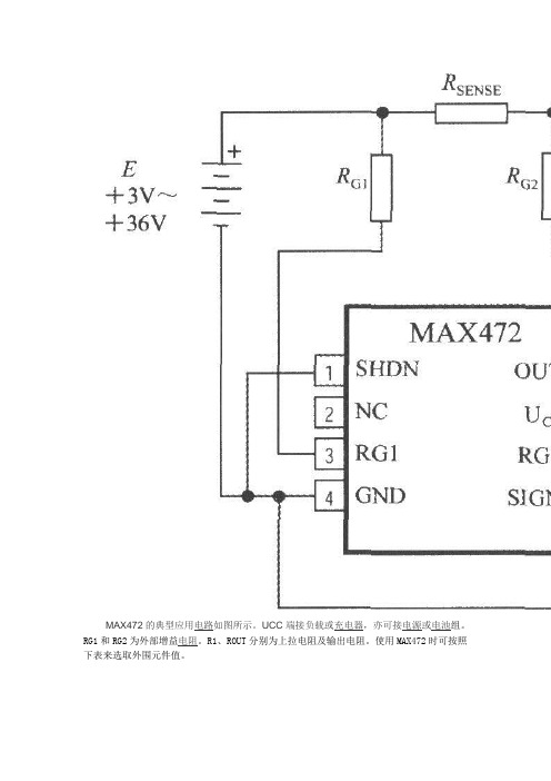
MAX472的典型应用电路如图所示。
UCC端接负载或充电器,亦可接电源或电池组。
RG1和RG2为外部增益电阻。
R1、ROUT分别为上拉电阻及输出电阻。
使用MAX472时可按照下表来选取外围元件值。
【收藏此页】【关闭】【返回】【打印】MP25P1171344:一、前言伴随着城市人口和建设规模的扩大,各种用电设备的增多,用电量越来越大,城市的供电设备经常超负荷运转,用电环境变得越来越恶劣,对电源的“考验”越来越严重。
据统计,每天,用电设备都要遭受 120 次左右各种的电源问题的侵扰,电子设备故障的 60% 来自电源 [7] 。
因此,电源问题的重要性日益凸显出来。
原先作为配角,资金投入较少的电源越来越受到厂商和研究人员的重视,电源技术遂发展成为一门崭新的技术。
而今,小小的电源设备已经融合了越来越多的新技术。
例如开关电源、硬开关、软开关、参数稳压、线性反馈稳压、磁放大器技术、数控调压、 PWM 、 SPWM 、电磁兼容等等。
实际需求直接推动电源技术不断发展和进步,为了自动检测和显示电流,并在过流、过压等危害情况发生时具有自动保护功能和更高级的智能控制,具有传感检测、传感采样、传感保护的电源技术渐成趋势,检测电流或电压的传感器便应运而生并在我国开始受到广大电源设计者的青睐,本文主要介绍 ABB 公司的电流传感器。
二、电流传感器的工作原理 [1]ABB 公司的电流传感器可以测量各种类型的电流,从直流电到几十千赫兹的交流电,其所依据的工作原理主要是霍尔效应,如图 1 所示。
当原边导线经过电流传感器时,原边电流 I P 会产生磁力线①,原边磁力线集中在磁芯②周围,内置在磁芯气隙中的霍尔电极③可产生和原边磁力线①成正比的大小仅几毫伏的电压,电子电路④可把这个微小的信号转变成副边电流 I S ⑤,并存在以下关系式其中, I S —副边电流;I P —原边电流;N P —原边线圈匝数;N S —副边线圈匝数;N P / N S —匝数比,一般取 N P =1 。
MAX471MAX472的中文资料大全

M A X471M A X472的中文资料大全(总4页)-本页仅作为预览文档封面,使用时请删除本页-MAX471/MAX472的特点、功能美国美信公司生产的精密高端电流检测放大器是一个系列化产品,有MAX471/MA X472、 MAX4172/MAX4173等。
它们均有一个电流输出端,可以用一个电阻来简单地实现以地为参考点的电流/电压的转换,并可工作在较宽电压内。
MAX471/MAX472具有如下特点:●具有完美的高端电流检测功能;●内含精密的内部检测电阻(MAX471);●在工作温度范围内,其精度为2%;●具有双向检测指示,可监控充电和放电状态;●内部检测电阻和检测能力为3A,并联使用时还可扩大检测电流范围;●使用外部检测电阻可任意扩展检测电流范围(MAX472);●最大电源电流为100μA;●关闭方式时的电流仅为5μA;●电压范围为3~36V;●采用8脚DIP/SO/STO三种封装形式。
MAX471/MAX472的引脚排列如图1所示,图2所示为其内部功能框图。
表1为MAX471/MAX472的引脚功能说明。
MAX471的电流增益比已预设为500μA/A,由于2kΩ的输出电阻(ROUT)可产生1V/A的转换,因此±3A时的满度值为3V.用不同的ROUT电阻可设置不同的满度电压。
但对于MAX471,其输出电压不应大于VRS+。
对于MAX472,则不能大于。
MAX471引脚图如图1所示,MAX472引脚图如图2所示。
MAX471/MAX472的引脚功能说明引脚名称功能MAX471MAX47211SHDN关闭端。
正常运用时连接到地。
当此端接高电平时,电源电流小于5μA2,3-RS+内部电流检测电阻电池(或电源端)。
“+”仅指示与SIGN输出有关的流动方向。
封装时已将2和3连在了一起-2空脚-3RG1增益电阻端。
通过增益设置电阻连接到电流检测电阻的电池端44GND地或电池负端55SIGN集电极开路逻辑输出端。
47204中文资料
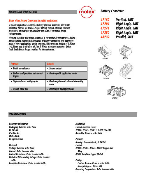
FEATURES AND SPECIFICATIONS SPECIIFICATIONS Battery Connector47182Vertical, SMT 47204Right Angle, SMT 47274Right Angle, SMT 47280Right Angle, SMT 48232Parallel, SMTMolex offers Battery Connectors for mobile applications.In mobile applications, battery efficiency plays an important part in the utilization time of the device. Proper battery contact, efficient electrical properties, physical size of connector are some of the major design considerations.Working together with major customers in the mobile device markets, Molex has developed a comprehensive range of battery connectors that addresses most of these applications design concerns. With working heights of 1.50mm to 5.50mm and circuit sizes of 2 to 5, Molex’s battery connectors brings forth flexibility in design solutions for the customers.4718247204472744823247280Reference InformationPackaging: Refer to order tableUL File No.:CSA File No.:Mates With:Designed In:mmElectricalVoltage: Refer to order tableCurrent: Refer to order tableContact Resistance: Refer to order tableDielectric Withstanding Voltage: Refer to ordertableInsulation Resistance: Refer to order tableMechanicalContact Insertion Force:47182, 47274, 47204 : 1.02N (0.67lb)Durability: Refer to order tablePhysicalHousing: Thoermoplastic, JL 94V-0Contact:47182, 47204, 47274, 48232 Copper (Cu)Alloy47280 Beryllium Copper (BeCu)Plating:Contact Area —Refer to order tableUnderplating—Nickel (Ni)Operating Temperature: Refer to order tableORDERING INFORMATIONBringing People & Technology Together, Worldwide SMVisit our Web site at Americas Headquarters 2222 Wellington Ct.Lisle, Illinois 60532 USA 1-800-78MOLEX amerinfo@Far East North Headquarters Yamato, Kanagawa, Japan 81-462-65-2324feninfo@Far East South Headquarters Jurong, Singapore 65-6-268-6868fesinfo@European Headquarters Munich, Germany 49-89-413092-0eurinfo@Corporate Headquarters 2222 Wellington Ct.Lisle, Illinois 60532 USA 630-969-4550MARKETS AND APPLICATIONS Order No. SNG-059©2006, MolexBattery Connector 47182Vertical, SMT 47204Right Angle, SMT 47274Right Angle, SMT 47280Right Angle, SMT 48232Parallel, SMT•Mobile phones •PDAs•Handheld GPS unitsMobile PhonesPDAsHandheld GPS。
DE2E3KY472MA3BM02;中文规格书,Datasheet资料

I Rated Value
Murata PN Code
Spec
Temperature Char.
E3
E, +20/-55%
Capacitance
472
4700pF
Capacitance Tol.
M
±20%
Safety Standard Certified Type
KY
X1,Y2: AC250V(r.m.s.)
Capacitors > Safety Standard Certified Ceramic Cap.
Data Sheet
Safety Standard Certified Type KY(Basic Insulation) (UL, CSA, IEC60384-14 ClassX1/Y2)
DE2E3KY472MA3BM02 (E, 4700pF, AC250V)
2. This datasheet has only typical specifications because there is no space for detailed specifications. Therefore, please approve our product specifications or transact the approval sheet for product specifications before ordering. 2011.7.7
RoHS regulation conformity parts
D max.
T max.
25.0 min. 3.0 max.
e
F±1.0
ød
Байду номын сангаас
Ratingrange:评级范围

Approval Standard And Recognized NO.CB Part Number Configuration :JY 102 K Y5P Y2(1) AC capacitors, safety(4) Type code: Y5P, Y5V,Y5U(1) (2) (3) (4) (5)(2) Rated capacitance (5) Class Y2(3) Tolerance on rated capacitance3JYH HSU Y2 SERIESINTRODUCTIONThese Ceramic Disc Capacitors are specifically designed for AC applications and meet the safety requirements of various safety standards agencies.These capacitors are ideal for acrossFEATURES:⊙Ideal for across the line applictions ⊙Compact size⊙Cost effective product⊙Safety standards recognized for AC applicationsCAPACITANCE AND DIMENSIONS:When ordering safety standard recognized ceramic capacitors please use the part number as noted aboveMARKINGJEC TYPE DESIGNATION or JD ( for Y1) 3 - DIGIT - SYSTEM : 472 = 4700 PF : 103 = 10000 PF CODE : K =Dimensions and Tolerance B = 3.0 mm max for AA d =0.55 mm ±0.05 mm F = 7.5 or 9.5 ±0.8 mm L =3 ~ 33 mm.◎ According as customer's request and size.Y2 , X1 ,AC300V , AC400V5新版1:新版2:加 KCWhether to put a KC logo according to customer's request按客户要求是否要加印 KC 标志MARKING : (FOR Y2)旧版6文件編號:P004 版 本:5 制訂日期:2014/02/20JECJY 102 KJEC JY 102 KJY 103 MJEC成品之編碼原則上以十五碼完成,亦以阿拉伯數字與英文字母混合編成,文件編號:P004碼至第十一碼與瓷片相同。
MAX16143、MAX16145、MAX16147和MAX16149监控芯片说明书

MAX16147WM75SA+MAX16147WM75SA+TGeneral DescriptionThe MAX16143, MAX16145, MAX16147, and MAX16149 are supervisory circuits that monitor their own supply voltages using a factory-set reset threshold that ranges from +2.3V to +11.6V. A manual reset (MR or MR ) input is included. The RESET (or RESET ) output has options for active-low, active-high, push-pull, or open-drain. The reset output asserts when the monitored voltage falls below the threshold voltage, and remains asserted until the monitored voltage has exceeded its threshold (plus hysteresis) for a time equal to the factory-set reset time-out period. Available reset timeout periods range from 30µs to 4.2s.The 5-pin SOT23 and 4-bump wafer-level packages (WLPs) offer compatibility with space-constrained environments. These ICs are fully specified over the -40°C to +125°C temperature range.Applications●Servers●Communications Equipment ●Industrial EquipmentOrdering Information appears at end of data sheet.19-100361; Rev 1; 6/18Benefits and Features●Factory-Set Reset Threshold Options from +2.3V to+11.6V ●Manual Reset Input• Active-High and Active-Low Trigger Options • Optional Internal Pullup or Pulldown• Fast (45µs) and Slow (50ms) Debounce Time Options ●Guaranteed Reset Valid to V CC ≥ 1.3V●Push-Pull and Open-Drain Reset Output Options• M AX16143: Open-Drain, Active-Low • MAX16145: Open-Drain, Active-High • MAX16147: Push-Pull, Active-Low • MAX16149: Push-Pull, Active-High ●Power-Supply Transient Immunity●-40°C to +125°C Operating Temperature Range ●SOT23-5 Package and 4-Bump WLPsSimplified Block DiagramClick here for production status of specific part numbers.MAX16143/MAX16145/MAX16147/MAX16149High-Voltage Supervisors with Manual Reset InputEVALUATION KIT AVAILABLEV CC to GND ..........................................................-0.3V to +15V MR or MR to GND .............-0.3V to lower of VCC + 0.3 or 6.0 V RESET or RESET to GND ....-0.3V to lower of V CC +0.3 or 6.0V Input/Output Current (All pins) ........................-20mA to +20mA Continuous Power Dissipation (Multilayer Board, SOT23, T A = +70°C, derate 3.9mW/°Cabove +70°C.) .............................................................312.6mWContinuous Power Dissipation (Multilayer Board,WLP , T A = +70°C, derate 9.7mW/°C above +70°C.) ....776mW Operating Temperature Range .........................-40°C to +125°C Storage Temperature Range ............................-65°C to +150°CSOT-23PACKAGE CODEU5+1Outline Number 21-0057Land Pattern Number90-0174Thermal Resistance, Single-Layer Board:Junction to Ambient (θJA )324.3Junction to Case (θJC )82Thermal Resistance, Four-Layer Board:Junction to Ambient (θJA )255.9Junction to Case (θJC )81WLPPACKAGE CODEW40E0+1Outline Number 21-100215Land Pattern NumberSee App Note 1891Thermal Resistance, Four-Layer Board:Junction to Ambient (θJA )103°C/W Junction to Case (θJC )N/A Absolute Maximum RatingsStresses beyond those listed under “Absolute Maximum Ratings” may cause permanent damage to the device. These are stress ratings only, and functional operation of the device at these or any other conditions beyond those indicated in the operational sections of the specifications is not implied. Exposure to absolute maximum rating conditions for extended periods may affect device reliability.Package thermal resistances were obtained using the method described in JEDEC specification JESD51-7, using a four-layer board. For detailed information on package thermal considerations, refer to /thermal-tutorial .For the latest package outline information and land patterns (footprints), go to /packages . Note that a “+”, “#”, or “-” in the package code indicates RoHS status only. Package drawings may show a different suffix character, but the drawing pertains to the package regardless of RoHS status.Package InformationMAX16143/MAX16145/ MAX16147/MAX16149High-Voltage Supervisors with Manual Reset Input(V CC = 2.3V to 14V, T J = T A = -40°C to +125°C, Typical values are at T A = 25°C unless otherwise noted. Limits over the operating temperature range and relevant supply voltage range are guaranteed by design, test, and characterization.)Note 2: Correct reset output voltage is guaranteed down to V CC = 1.3V.Note 3: During power-up, the internal regulator takes 2ms. Power-up time must be added to reset timeout period.PARAMETERSYMBOL CONDITIONSMIN TYPMAX UNITSOperating Voltage RangeV CCCorrect threshold detection3.314V MAX16143, MAX16147 (active-low). Correct reset state for supply ramp time ≥ 20µs. (Note 2) 1.314MAX16145, MAX16149 (active-high). Correct reset state for supply ramp time ≥ 1ms.214Supply CurrentI CC V CC ≤ V TH + 150mV2555µA Reset Threshold AccuracyV TH_ACC-1.5+1.5%Reset Threshold HysteresisHysteresis option Q, V CC rising0.5%V THHysteresis option R, V CC rising 1Hysteresis option S, V CC rising 3Hysteresis option T, V CC rising5V CC to Reset Output Delay t RDV CC falling at 10mV/µs from (V CC + 100mV) to (V CC - 100mV)15µs Reset Timeout Period Accuracy (Note 3)Variation from nominal t RP -25+25%Output Voltage Low V OL V CC ≥ 1.7V, I SINK = 3.2mA 0.4V 1.3V ≤ V CC < 1.7V, I SINK = 100µA 0.4Output Voltage High V OH MAX16147/MAX16149, I SOURCE = 10μA 2.4 3.15V Output CurrentI OH V OH = 2.5V255080µA Open-Drain Output Leakage CurrentMAX16143/MAX161451µA Manual Reset Debounce Timet DB Active-low or active-high manual reset 4570µs 5070ms Manual Reset Minimum Input Pulse Width t PW Edge-triggered manual reset option.—µs MR Internal Pullup Resis-tanceR PU MR option F or H 50kΩMR Internal Pulldown Re-sistanceR PD MR option B or D 50kΩInput Voltage Low V IL MR, MR 0.7V Input Voltage High V IH MR, MR1.7V Input CurrentMR, MR . Internal pullup resistor not connected.-150+150nA Electrical CharacteristicsMAX16143/MAX16145/ MAX16147/MAX16149High-Voltage Supervisors with Manual Reset Input(T A = 25°C unless otherwise noted.)Typical Operating CharacteristicsMAX16143/MAX16145/ MAX16147/MAX16149High-Voltage Supervisors with Manual Reset Input(T A = 25°C unless otherwise noted.)Typical Operating Characteristics (continued)1101001000MAXIMUM V CC TRANSIENT DURATION vs. OVERDRIVEtoc112V/div20ms/divRST 2V/div 2V/divV CC = 12Vtoc09MAX16143/MAX16145/ MAX16147/MAX16149High-Voltage Supervisors with Manual Reset Input(T A = 25°C unless otherwise noted.)Typical Operating Characteristics (continued)toc162ms/divV CC RISE TIME = 10ms1V/divRESETtoc14500µs/div1V/divV BACKUPV CC RISE TIME = 100µs1V/divRESETtoc1720ms/div1V/divCCV CC RISE TIME = 100ms1V/divtoc151V/divV CC RISE TIME = 1msMAX16143/MAX16145/ MAX16147/MAX16149High-Voltage Supervisors with Manual Reset InputPINNAME FUNCTIONSOT23WLP 1A1RESET, RESET Reset Output. RESET asserts when V CC falls below the factory-set threshold or when the manual reset is triggered. RESET deasserts after the factory-set reset timeout when V CC goes above its set threshold or when MR is released.2, 4B2GND Ground3B1MR, MR Manual Reset Input. See Manual Reset Input section for more detail.5A2V CCSupply Voltage Input. Bypass V CC to ground with a 0.1µF capacitor.Pin ConfigurationPin DescriptionMAX16143/MAX16145/ MAX16147/MAX16149High-Voltage Supervisors with Manual Reset InputDetailed DescriptionThe MAX16143/MAX16145/MAX16147/MAX16149 aresupervisory circuits that monitor their V CC voltage from+2.3V to +11.6V using factory-set reset threshold andoffer manual reset capability. The MAX16143/MAX16145feature an open-drain reset output, while the MAX16147/MAX16149 feature a push-pull reset output. The resetoutput asserts and remains asserted for the reset timeoutafter the V CC voltage exceeds its threshold. All devicesare offered with reset timeout periods ranging from 30μsto 4200ms. See Table 1 for available options. The resetoutput is guaranteed to be in valid logic state down toV CC = 1.3V.V CC ThresholdThe MAX16143/MAX16145/MAX16147/MAX16149operate with a V CC supply voltage from +3.3V to +14V,with monitoring range of +2.3V to +11.6V. V CC has arising threshold of V TH + V HYST and a falling thresholdof V TH. See Tables 2 and 3 for available threshold andhysteresis options. When V CC rises above V TH + V HYSTand the manual reset input is in an inactive state, RESETdeasserts after the reset timeout period (t RP). See thetiming diagram in Figure 1. When V CC falls below V TH,the reset output asserts low after a fixed delay (t RD).Table 1. Reset Timeout OptionsTable 2. V CC Threshold OptionsSUFFIXRESET TIMEOUTPERIODUNIT T A = 25°CT A = -40°Cto +125°CTYP MIN MAXA30——µs B 1.50 1.125 1.875ms C3 2.25 3.75ms D6 4.57.5ms E12915ms F241830ms G5037.562.5ms H10075125ms I150112.5187.5ms J225168.8281.3ms K300225375ms L450337.5562.5ms M600450750ms N10007401250ms O200015002500ms P420031505250ms SUFFIX1.5%UNITTYP MIN MAXY611.48411.60011.716V Y511.38511.50011.615V Y411.28611.40011.514V Y311.18711.30011.413V Y211.08811.20011.312V Y110.98911.10011.211V Y010.8911.00011.11V X710.59310.70010.807V X610.49410.600107.06V X510.39510.50010.605V 009.910.00010.1V 959.4059.5009.595V 908.919.0009.09V 858.4158.5008.585V 807.928.0008.08V 757.4257.5007.575V70 6.937.0007.07V65 6.435 6.500 6.565V60 5.94 6.000 6.06V55 5.445 5.500 5.555V48 4.752 4.800 4.848V47 4.653 4.700 4.747V46 4.554 4.600 4.646V45 4.455 4.500 4.545V44 4.356 4.400 4.444V43 4.257 4.300 4.343V42 4.158 4.200 4.242V41 4.059 4.100 4.141V40 3.960 4.000 4.040V39 3.861 3.900 3.939V38 3.762 3.800 3.838V37 3.663 3.700 3.737V36 3.564 3.600 3.636V35 3.465 3.500 3.535V34 3.366 3.400 3.434V33 3.267 3.300 3.333V32 3.168 3.200 3.232V31 3.069 3.100 3.131V30 2.970 3.000 3.030V29 2.871 2.900 2.929VMAX16143/MAX16145/ MAX16147/MAX16149High-Voltage Supervisors with Manual Reset InputReset OutputThe MAX16143/MAX16145 feature open-drain reset outputs, while the MAX16147/MAX16149 feature push-pull reset outputs. For proper operation, connect the reset output of the MAX16143 and the MAX16145 to V CC , or external voltage with a pullup resistor. The reset output of the MAX16147 and the MAX16149 are internally connected to a 2.5V or 3V regulator.Manual Reset InputThe MAX16143/MAX16145/MAX16147/MAX16149 include a manual reset input (MR, MR ) that allows initiating system reset using external signal or push-button switch. The manual reset input is available in active-low, active-high or edge-triggered option. The active-low (MR ) and active-high (MR) inputs feature either 45μs or 50ms debounce timing option to help filter out noise during manual reset transitioning from inactive to active state. In addition, the manual reset input is factory-programmable to have a pull up/pull down resistor or be left floating. See Table 4 and Table 5 for available options.Table 2. V CC Threshold Options (continued)Table 3. V CC Threshold Hysteresis OptionsTable 4. MAX16143/MAX16145 Manual Reset Configuration OptionsSUFFIX 1.5%UNIT TYP MIN MAX 28* 2.772 2.800 2.828V 27 2.673 2.700 2.727V 26* 2.574 2.600 2.626V 25 2.475 2.500 2.525V 24 2.376 2.400 2.424V 232.2772.3002.323VSUFFIX HYSTERSISQ 0.5%R 1%S 3%T5%SUFFIXLEVEL HIGH/LOWDEBOUNCE TIME (NA = EDGE TRIGGER)PULLUP/PULLDOWN A H 45µs NOT CONNECTEDB H 45µs PULLDOWNC H 50ms NOT CONNECTEDD H 50ms PULLDOWNE L 45µs NOT CONNECTEDF L 45µs PULLUPG L 50ms NOT CONNECTEDH L 50ms PULLUP J H N/A NOT CONNECT K H N/A PULLDOWN L L N/A NOT CONNECTEDMLN/APULL UPMAX16143/MAX16145/ MAX16147/MAX16149High-Voltage Supervisors with Manual Reset InputTable 5. MAX16147/MAX16149 Manual Reset and RESET Configuration OptionsSUFFIX LEVELHIGH/LOW DEBOUNCE TIME(NA = EDGETRIGGER)MR/MRPULLUP/PULLDOWNRESETPULLUPVOLTAGEA H45µs NOT CONNECTED3VB H45µs PULLDOWN3VC H50ms NOT CONNECTED3VD H50ms PULLDOWN3VE L45µs NOT CONNECTED3VF L45µs PULLUP3VG L50ms NOT CONNECTED3VH L50ms PULLUP3VJ H N/A NOT CONNECTED 2.5VK H N/A PULLDOWN 2.5VL H N/A NOT CONNECTED 2.5VM H N/A PULLUP 2.5VN L45µs NOT CONNECTED 2.5VO L45µs PULLUP 2.5VP L50ms NOT CONNECTED 2.5VQ L50ms PULLUP 2.5VR H N/A NOT CONNECTED3VS H N/A PULLDOWN3VT L N/A NOT CONNECTED3VU L N/A PULLUP3VV H N/A NOT CONNECTED 2.5VW H N/A PULLDOWN 2.5VX L N/A NOT CONNECTED 2.5VY L N/A PULLUP 2.5V MAX16147/MAX16149with Manual Reset InputApplications InformationReset OutputThe MAX16143/MAX16145/MAX16147/MAX16149 are microprocessor supervisory circuits that assert a reset to prevent code-execution errors during power-up, power-down, and brownout conditions. The reset output asserts when the V CC voltage falls below the factory-set threshold, V TH . The reset output de-asserts after the reset timeout (t RP ) when V CC voltage rises above the reset threshold plus the hysteresis voltage, (V TH + V HYST ). The reset output is guaranteed to be at the correct logic voltage for VCC voltage down to 1.3V. See Figure 1 for details.Manual Reset Input (MR)Many systems require manual reset capability, allowing the operator, a test technician, or external logic circuitry to initiate a reset. The MAX16143/MAX16145/MAX16147/MAX16149 provide this capability by featuring an manual reset input (MR). When a manual reset is initiated, the reset output asserts and remain asserted as long as the manual reset input is in active state. Reset deasserts after reset timeout when the manual reset input is released. Figure 1 shows the behavior of the manual reset configured as active-low, with 50kΩ pull (MR ). See Selector Guide for available options.Depending on the application, the manual reset input is factory-programmable to have either an internal pullup resistor, pulldown resistor of 50kΩ (typ), or be left floating.The pullup resistor allows the manual reset input to be left unconnected if not used. An external pullup resistor is required if the manual reset input option chosen does not have an internal pullup resistor. The maximum input voltage on MR is 5.5V.An alternative is to use a normally open momentary switch connected from MR (active-low) to GND, or from MR (active-high) to a logic-high voltage to create a manual-reset function. If a Long Debounce version is used, external debounce circuitry is not required, but an external pullup or pulldown will be required if a version without an internal resistor is used. If the manual reset input is driven from long cables, or the IC is used in a noisy environment, connect a 0.1μF capacitor from MR /MR to GND in order to provide additional noise immunity.Negative-Going V CC Transients ProtectionThese supervisory circuits are relatively immune to short-duration, negative-going V CC transients (glitches). The Maximum Transient Duration vs. Reset Threshold Overdrive graph (in the Typical Operating Characteristics section) shows the typical transient pulse width and amplitude required to trigger a reset. The reset threshold overdrive specifies how far the pulse falls below the actual reset threshold, and the maximum transient duration specifies the width of the pulse as it crosses the reset threshold. If a pulse occurs in the region above the curve, a reset triggers. If a pulse occurs in the region below the curve, a reset does not trigger.Figure 1. RESET and MR Timing DiagramMAX16147/MAX16149with Manual Reset InputMAX16147/MAX16149with Manual Reset Input*Future product—Contact factory for availability.+ Denotes a lead(Pb)-free/RoHS-compliant package. T Denotes tape-and-reel.PARTTEMP RANGE PIN-PACKAGEMAX16143_ _ _ _ _+T*-40°C to +125°C 4 WLP MAX16145_ _ _ _ _ T*-40°C to +125°C 4 WLP MAX16147WM75SA+T -40°C to +125°C 4 WLP MAX16149_ _ _ _ _T*-40°C to +125°C4 WLPTypical Application CircuitOrdering InformationMAX16147/MAX16149with Manual Reset InputREVISION NUMBERREVISION DATEDESCRIPTIONPAGES CHANGED06/18Initial release—16/18Updated Simplified Block Diagram and Ordering Information table1, 13Revision HistoryMaxim Integrated cannot assume responsibility for use of any circuitry other than circuitry entirely embodied in a Maxim Integrated product. No circuit patent licenses are implied. Maxim Integrated reserves the right to change the circuitry and specifications without notice at any time. The parametric values (min and max limits) shown in the Electrical Characteristics table are guaranteed. Other parametric values quoted in this data sheet are provided for guidance.MAX16147/MAX16149with Manual Reset InputFor pricing, delivery, and ordering information, please contact Maxim Direct at 1-888-629-4642, or visit Maxim Integrated’s website at .MAX16147WM75SA+MAX16147WM75SA+T。
ZST6000光伏逆变器综合测试仪入门手册V1.02

致远电子
安全须知
本仪器的使用涉及到高压,为防止电击或其它危险造成的人员伤亡,在安装、使用或 维修本产品之前,请务必仔细阅读、并完全理解“安全须知”章节的相关内容。 为保证您能正确安全地使用本仪器, 请务必遵守以下注意事项。 如果未遵守本手册指定 的方法操作本仪器, 可能会损坏本仪器的保护功能。 因违反以下注意事项操作仪器所引起的 损伤,广州致远电子股份有限公司概不承担责任。
产品入门手册 << I
致远电子
注意搬运安全
ZST6000 入门手册
为避免仪器在搬运过程中滑落,造成仪器面板上的按键、旋钮或接口等部件损坏,请注 意搬运安全。
警示标志
注意符号表示存在危险。提示用户对某一过程、操作方法或类似情况 进行操作时,如果不能正确执行或遵守规则,则可能对产品造成损坏或者 丢失重要数据。在完全阅读和充分理解注意所要求的事项之前,请不要继 续操作。 警告符号表示存在严重危险。提示用户对某一过程、操作方法或类似 情况进行操作时,如果不能正确执行或遵守规则,则可能造成人身伤害甚 至死亡。在完全阅读和充分理解警告所要求的事项之前,请务必停止操作。
安全信息
光伏逆变器综合测试仪安全符号如下所示。
小心,危险
CE 认证
地端子
小心,电击危险
请勿将使用过的 电池丢入垃圾桶
可回收利用
CAT Ⅱ(1000V)IEC 测量Ⅱ类,输入可连接到归属到Ⅱ类过电压条件下的电源 ( 最大 1000VAC)。 一般注意事项 针对人身安全与设备保护,列出注意事项如下所述: 保护功能有缺陷。在使用仪器之前,请对保护功能进行确认。如发现 保护接地或保险丝有缺陷,请勿继续使用本仪器; 请勿拆卸仪器的机箱。仪器内部有高压,非常危险。若要对仪器内部 进行检查和调试,请咨询广州致远电子股份有限公司; 出现异味或冒烟时。出现机体冒烟或散发异味等异常情况时,请直接 关闭电源,从插座拔掉电源插头,并切断连接在输入端子的测量回路 的电源。发生异常情况时,请咨询致远公司; 勿在易燃环境下操作仪器。请勿在含有易燃易爆液体或气体的环境里 使用本仪器; 请勿损坏电源线。请勿将物品摆放在电源线上,并使电源线远离热源。 将电源插头从插座拔出时,请勿拉扯电线,而应手持插头拔出。电源 线有破损时,请在确认好零件编号后再向经销商订购;
MAX472中文资料

_______________General DescriptionThe MAX471/MAX472 are complete, bidirectional, high-side current-sense amplifiers for portable PCs, tele-phones, and other systems where battery/DC power-line monitoring is critical. High-side power-line monitoring is especially useful in battery-powered sys-tems, since it does not interfere with the ground paths of the battery chargers or monitors often found in “smart” batteries.The MAX471 has an internal 35m Ωcurrent-sense resis-tor and measures battery currents up to ±3A. For appli-cations requiring higher current or increased flexibility,the MAX472 functions with external sense and gain-set-ting resistors. Both devices have a current output that can be converted to a ground-referred voltage with a single resistor, allowing a wide range of battery volt-ages and currents.An open-collector SIGN output indicates current-flow direction, so the user can monitor whether a battery is being charged or discharged. Both devices operate from 3V to 36V, draw less than 100µA over tempera-ture, and include a 18µA max shutdown mode.________________________ApplicationsPortable PCs:Notebooks/Subnotebooks/Palmtops Smart Battery Packs Cellular Phones Portable PhonesPortable Test/Measurement Systems Battery-Operated Systems Energy Management Systems____________________________Featureso Complete High-Side Current Sensing o Precision Internal Sense Resistor (MAX471)o 2% Accuracy Over Temperature o Monitors Both Charge and Dischargeo 3A Sense Capability with Internal Sense Resistor (MAX471)o Higher Current-Sense Capability with External Sense Resistor (MAX472)o 100µA Max Supply Current o 18µA Max Shutdown Mode o 3V to 36V Supply Operation o 8-Pin DIP/SO Packages______________Ordering InformationMAX471/MAX472Precision, High-Side Current-Sense Amplifiers________________________________________________________________Maxim Integrated Products1_________________Pin Configurations__________Typical Operating Circuit19-0335; Rev 2; 12/96For free samples & the latest literature: , or phone 1-800-998-8800M A X 471/M A X 472Precision, High-SideCurrent-Sense AmplifiersABSOLUTE MAXIMUM RATINGSELECTRICAL CHARACTERISTICS—MAX471(RS+ = +3V to +36V, T A = T MIN to T MAX , unless otherwise noted. Typical values are at T A = +25°C.)Stresses beyond those listed under “Absolute Maximum Ratings” may cause permanent damage to the device. These are stress ratings only, and functional operation of the device at these or any other conditions beyond those indicated in the operational sections of the specifications is not implied. Exposure to absolute maximum rating conditions for extended periods may affect device reliability.Supply Voltage, RS+, RS-, V CC to GND....................-0.3V, +40V RMS Current, RS+ to RS- (MAX471 only)..........................±3.3A Peak Current, (RS+ to RS-)......................................see Figure 5Differential Input Voltage, RG1 to RG2 (MAX472 only) .....±0.3V Voltage at Any Pin Except SIGNMAX471 only...........................................-0.3V to (RS+ - 0.3V)MAX472 only..........................................-0.3V to (V CC + 0.3V)Voltage at SIGN......................................................-0.3V to +40V Current into SHDN, GND, OUT, RG1, RG2, V CC ................±50mA Current into SIGN.................................................+10mA, -50mAContinuous Power Dissipation (T A = +70°C)MAX471 (Note 1):Plastic DIP (derate 17.5mW/°C above +70°C)..................1.4W SO (derate 9.9mW/°C above +70°C).............................791mW MAX472 :Plastic DIP (derate 9.09mW/°C above +70°C)..............727mW SO (derate 5.88mW/°C above +70°C)...........................471mW Operating Temperature RangesMAX47_C_A........................................................0°C to +70°C MAX47_E_A.....................................................-40°C to +85°C Junction Temperature Range............................-60°C to +150°C Storage Temperature Range.............................-60°C to +160°C Lead Temperature (soldering, 10sec).............................+300°CNote 1:Due to special packaging considerations, MAX471 (DIP, SO) has a higher power dissipation rating than the MAX472. RS+and RS- must be soldered to large copper traces to achieve this dissipation rating.MAX471/MAX472Precision, High-Side Current-Sense Amplifiers_______________________________________________________________________________________3ELECTRICAL CHARACTERISTICS—MAX472(V CC = +3V to +36V, RG1 = RG2 = 200Ω, T A = T MIN to T MAX , unless otherwise noted. Typical values are at T A = +25°C.)Note 2:V OS is defined as the input voltage (V SENSE ) required to give minimum I OUT .Note 3:V SENSE is the voltage across the sense resistor.M A X 471/M A X 472Precision, High-SideCurrent-Sense Amplifiers 4_________________________________________________________________________________________________________________________________Typical Operating Characteristics(Typical Operating Circuit (MAX471) or circuit of Figure 4, RG1 = RG2 = 200Ω, R OUT = 2k Ω(MAX472), T A = +25°C, unless otherwise noted.)6535SUPPLY CURRENT vs. SUPPLY VOLTAGE40V RS+ (V)S U P P L Y C U R R E N T (µA )212415189123627303336455055602.500.52.0I S H D N (µA )1.51.0SHUTDOWN CURRENT vs. SUPPLY VOLTAGEV RS+(V)2124151891236273033364-2SIGN THRESHOLD vs. SUPPLY VOLTAGE-1S I G N T H R E S H O L D (m A )2124151891236273033360123V RS+ (V)0.6O F F S E T C U R R E N T (µA )MAX471NO-LOAD OFFSET CURRENT vs.SUPPLY VOLTAGEV RS+ (V)2124151891236273033360.81.01.21.41.61.82.02.22.428-4080TEMPERATURE (°C)R E S I S T A N C E (m Ω)2030-206040M A X 1471-07MAX471RS+ TO RS- RESISTANCE vs.TEMPERATURE3234363840-120.010.10MAX471ERROR vs. LOAD CURRENTI LOAD (A)E R R O R (%)110-15-6-9-303691215400.01101000MAX471POWER-SUPPLY REJECTION RATIOvs. FREQUENCYPOWER-SUPPLY FREQUENCY (kHz)P S R R (%)1100353025201510500.103.00MAX472NO-LOAD OUTPUT ERROR vs.SUPPLY VOLTAGE0.5V CC (V)IO U T (µA )2124151891236273033361.01.52.02.50.70E R R O R (%)MAX472ERROR vs. SUPPLY VOLTAGEV CC (V)2124151891236273033360.800.901.001.10MAX471/MAX472Precision, High-Side Current-Sense Amplifiers_______________________________________________________________________________________525-250.1101000MAX472ERROR vs. SENSE VOLTAGEV SENSE (mV)E R R O R (%)1550-5-1511001mA10mA100mA1A0.100.20.30.40.5MAX471 NOISE vs. LOAD C URRENTI SENSEI O U T N O I S E (µA R M S )M A X 471-15____________________________Typical Operating Characteristics (continued)(Typical Operating Circuit (MAX471) or circuit of Figure 4, RG1 = RG2 = 200Ω, R OUT = 2k Ω(MAX472), T A = +25°C, unless otherwise noted.)100µs/divV CC = 10V, R OUT = 2k Ω 1%, SIGN PULL-UP = 50k Ω 1%LOAD CURRENT 50mA/div V OUT 50mV/divMAX4710mA to 100mA TRANSIENT RESPONSE0A10µs/divI LOAD = 1A, R OUT = 2k Ω 1%V OUT500mV/div MAX471 START-UP DELAY V SHDN 5V/div10µs/divR OUT = 2k Ω 1%I LOAD 1A/divMAX4710A TO 3A TRANSIENT RESPONSEV OUT 10mV/div100µs/divV CC = 10V, R OUT = 2k Ω 1%, SIGN PULL-UP = 50k Ω 1%LOAD CURRENT 100mA/div50mA/div V OUT 50mV/divMAX471-100mA to +100mA TRANSIENT RESPONSESIGN 50mV/div0AM A X 471/M A X 472_______________Detailed DescriptionThe MAX471 and MAX472 current-sense amplifier’s unique topology allows a simple design to accurately monitor current flow. The MAX471/MAX472 contain two amplifiers operating as shown in Figures 1 and 2. The battery/load current flows from RS+ to RS- (or vice versa) through R SENSE . Current flows through either RG1 and Q1 or RG2 and Q2, depending on the sense-resistor current direction. Internal circuitry, not shown in Figures 1 and 2, prevents Q1 and Q2 from turning on at the same time. The MAX472 is identical to the MAX471, except that R SENSE and gain-setting resistors RG1 and RG2 are external (Figure 2).To analyze the circuit of Figure 1, assume that current flows from RS+ to RS- and that OUT is connected to GND through a resistor. In this case, amplifier A1 is active and output current I OUT flows from the emitter of Q1. Since no current flows through RG2 (Q2 is off), the negative input of A1 is equal to V SOURCE - (I LOAD x R SENSE ). The open-loop gain of A1 forces its positive input to essentially the same level as the negative input.Therefore, the drop across RG1 equals I LOAD x R SENSE . Then, since I OUT flows through Q1 and RG (ignoring the extremely low base currents), I OUT x RG1= I LOAD x R SENSE , or:I OUT = (I LOAD x R SENSE )/ RG1Current OutputThe output voltage equation for the MAX471/MAX472 is given below. In the MAX471, the current-gain ratio has been preset to 500µA/A so that an output resistor (R OUT ) of 2k Ωyields 1V/A for a full-scale value of +3V at ±3A. Other full-scale voltages can be set with differ-ent R OUT values, but the output voltage can be no greater than V RS+- 1.5V for the MAX471 or V RG_- 1.5V for the MAX472.V OUT = (R SENSE x R OUT x I LOAD ) / RGwhere V OUT = the desired full-scale output voltage,I LOAD = the full-scale current being sensed, R SENSE =the current-sense resistor, R OUT = the voltage-setting resistor, and RG = the gain-setting resistor (RG = RG1= RG2).The above equation can be modified to determine the R OUT required for a particular full-scale range:R OUT = (V OUT x RG) / (I LOAD x R SENSE )For the MAX471, this reduces to:R OUT = V OUT / (I LOAD x 500µA/A)OUT is a high-impedance current-source output that can be connected to other MAX471/MAX472 OUT pinsPrecision, High-SideCurrent-Sense Amplifiers 6_____________________________________________________________________________________________________________________________________________________Pin DescriptionMAX471/MAX472Precision, High-Side Current-Sense Amplifiers_______________________________________________________________________________________7Figure 1. MAX471 Functional DiagramFigure 2. MAX472 Functional DiagramM A X 471/M A X 472for current summing. A single scaling resistor is required when summing OUT currents from multiple devices (Figure 3). Current can be integrated by con-necting OUT to a capacitive load.SIGN OutputThe current at OUT indicates magnitude. The SIGN out-put indicates the current’s direction. Operation of the SIGN comparator is straightforward. When Q1 (Figures 1 and 2) conducts, the output of A1 is high while A2’s output is zero. Under this condition, a high SIGN output indicates positive current flow (from RS+ to RS-). In bat-tery-operated systems, this is useful for determining whether the battery is charging or discharging. The SIGN output may not correctly indicate if the load cur-rent is such that I OUT is less than 3.5µA. The MAX471’s SIGN output accurately indicates the direction of cur-rent flow for load currents greater than 7mA.SIGN is an open-collector output (sinks current only),allowing easy interface with logic circuits powered from any voltage. Connect a 100k Ωpull-up resistor from SIGN to the logic supply. The convention chosen for the polarity of the SIGN output ensures that it draws no current when the battery is being discharged. If current direction is not needed, float the SIGN pin.ShutdownWhen SHDN is high, the MAX471/MAX472 are shut down and consume less than 18µA. In shutdown mode,SIGN is high impedance and OUT turns off.__________Applications InformationMAX471The MAX471 obtains its power from the RS- pin. This includes MAX471 current consumption in the total sys-tem current measured by the MAX471. The small drop across R SENSE does not affect the MAX471’s perfor-mance.Resistor SelectionSince OUT delivers a current, an external voltage gain-setting resistor (R OUT to ground) is required at the OUT pin in order to get a voltage. R SENSE is internal to the MAX471. RG1 and RG2 are factory trimmed for an out-put current ratio (output current to load current) of 500µA/A. Since they are manufactured of the same material and in very close proximity on the chip, they provide a high degree of temperature stability. Choose R OUT for the desired full-scale output voltage up to RS-- 1.5V (see the Current Output section).Precision, High-SideCurrent-Sense Amplifiers 8_______________________________________________________________________________________Figure 3. Paralleling MAX471s to Sense Higher Load Current Figure 4. MAX472 Standard Application CircuitPeak Sense CurrentThe MAX471’s maximum sense current is 3A RMS . For power-up, fault conditions, or other infrequent events,MAX472R SENSE , RG1, and RG2 are externally connected on the MAX472. V CC can be connected to either the load/charge or power-source/battery side of the sense resistor. Connect V CC to the load/charge side of R SENSE if you want to include the MAX472 current drain in the measured current.Suggested Component Valuesfor Various ApplicationsThe general circuit of Figure 4 is useful in a wide variety of applications. It can be used for high-current applica-tions (greater than 3A), and also for those where the full-scale load current is less than the 3A of the MAX471.Table 1 shows suggested component values and indi-cates the resulting scale factors for various applications required to sense currents from 100mA to 10A.Higher or lower sense-current circuits can also be built.Select components and calculate circuit errors using the guidelines and formulas in the following section.R SENSEChoose R SENSE based on the following criteria:a)Voltage Loss: A high R SENSE value will cause the power-source voltage to degrade through IR loss.For least voltage loss, use the lowest R SENSE value.b)Accuracy: A high R SENSE value allows lower currents to be measured more accurately. This is because offsets become less significant when the sense voltage is larger.c)Efficiency and Power Dissipation:At high current levels, the I 2R losses in R SENSE may be significant.Take this into consideration when choosing the resistor value and power dissipation (wattage) rat-ing. Also, if the sense resistor is allowed to heat up excessively, its value may drift.d)Inductance:If there is a large high-frequency com-ponent to I SENSE , you will want to keep inductance low. Wire-wound resistors have the highest induc-tance, while metal film is somewhat better. Low-inductance metal-film resistors are available. Instead of being spiral wrapped around a core, as in metal-film or wire-wound resistors, these are a straight band of metal. They are made in values under 1Ω.e)Cost:If the cost of R SENSE becomes an issue, you may want to use an alternative solution, as shown in Figure 6. This solution uses the PC board traces to create a sense resistor. Because of the inaccuracies of the copper “resistor,” you will need to adjust the full-scale current value with a potentiometer. Also,the resistance temperature coefficient of copper is fairly high (approximately 0.4%/°C), so systems that experience a wide temperature variance should take this into account.MAX471/MAX472Precision, High-Side Current-Sense AmplifiersTable 1. Suggested Component Values for the MAX472M A X 471/M A X 472In Figure 6, assume the load current to be measured is 10A and that you have determined a 0.3 inch wide, 2ounce copper to be appropriate. The resistivity of 0.1inch wide, 2 ounce copper is 30m Ω/ft (see Note 4). For 10A you may want R SENSE = 5m Ωfor a 50mV drop at full scale. This resistor will require about 2 inches of 0.1inch wide copper trace.RG1 and RG2Once R SENSE is chosen, RG1 and RG2 can be chosen to define the current-gain ratio (R SENSE /RG). Choose RG = RG1 = RG2 based on the following criteria:a)1ΩInput Resistance.The minimum RG value is lim-ited by the 1Ωinput resistance, and also by the out-put current limitation (see below). As RG is reduced,the input resistance becomes a larger portion of the total gain-setting resistance. With RG = 50Ω, the input resistance produces a 2% difference between the expected and actual current-gain ratio. This is a gain error that does not affect linearity and can be removed by adjusting RG or R OUT .b)Efficiency.As RG is reduced, I OUT gets larger for a given load current. Power dissipated in R OUT is not going to the load, and therefore reduces overall effi-ciency. This is significant only when the sense cur-rent is small.c)Maximum Output Current Limitation.I OUT is limit-ed to 1.5mA, requiring RG ≥V SENSE / 1.5mA. For V SENSE = 60mV, RG must be ≥40Ω.d)Headroom.The MAX472 requires a minimum of 1.5V between the lower of the voltage at RG1 or RG2 (V RG_) and V OUT . As RG becomes larger, the voltage drop across RG also becomes larger for a given I OUT . This voltage drop further limits the maxi-mum full-scale V OUT . Assuming the drop across R SENSE is small and V CC is connected to either side of R SENSE , V OUT (max) = V CC - (1.5V + I OUT (max) x RG).e)Output Offset Error at Low Load rge RG values reduce I OUT for a given load current. As I OUT gets smaller, the 2.5µA max output offset-error current becomes a larger part of the overall output current. Keeping the gain high by choosing a low value for RG minimizes this offset error.f)Input Bias Current and Input Bias Current Mismatching.The size of RG also affects the errors introduced by the input bias and input bias mis-matching currents. After selecting the ratio, check tomake sure RG is small enough that I B and I OS do not add any appreciable errors. The full-scale error is given by:% Error = (RG1 - RG2) x I B + I OS x RG x 100I FS x R SENSEwhere RG1 and RG2 are the gain resistors, I B is the bias current, I OS is the bias-current mismatch, I FS is the full-scale current, and R SENSE is the sense resistor.Assuming a 5A load current, 10m ΩR SENSE , and 100ΩRG, the current-gain ratio is 100µA/A, yielding a full-scale I OUT of 500µA. Using the maximum values for I B (20µA) and I OS (2µA), and 1% resistors for RG1 and RG2 (RG1 - RG2 = 2Ω), the worst-case error at full scale calculates to:2Ωx 20µA + 100Ωx 2µA = 0.48%5m Ωx 5AThe error may be reduced by: a) better matching of RG1 and RG2, b) increasing R SENSE , or c) decreasing RG.Current-Sense Adjustment (Resistor Range, Output Adjust)Choose R OUT after selecting R SENSE , RG1, and RG2.Choose R OUT to obtain the full-scale voltage youPrecision, High-SideCurrent-Sense Amplifiers 10______________________________________________________________________________________Note 4:Printed Circuit Design, by Gerald L. Ginsberg; McGraw-Hill, Inc.; page 185.Figure 6. MAX472 Connections Showing Use of PC Board Tracerequire, given the full-scale I OUT determined by R SENSE, RG1, and RG2. The high compliance of OUT permits using R OUT values up to 10kΩwith minimal error. Values above 10kΩare not usually recommend-ed. The impedance of OUT’s load (e.g., the input of an op amp or ADC) must be much greater than R OUT (e.g., 100 x R OUT) to avoid degrading the measure-ment accuracy.High-Current Measurement The MAX472 can achieve higher current measurements than the MAX471 can. Low-value sense resistors may be paralleled to obtain even lower values, or the PC board trace may be adjusted for any value.An alternative method is to connect several MAX471s in parallel and connect the high-impedance current-source OUT pins together to indicate the total system current (Figure 3). Pay attention to layout to ensure equal IR drops in the paralleled connection. This is necessary to achieve equal current sharing.Power-Supply Bypassing and Grounding The MAX471 has been designed as a “high side” (posi-tive terminal) current monitor to ease the task of grounding any battery charger, thermistor, etc. that may be a part of the battery pack. Grounding the MAX471 requires no special precautions; follow the same cautionary steps that apply to the system as a whole. High-current systems can experience large volt-age drops across a ground plane, and this drop may add to or subtract from V OUT. For highest current-mea-surement accuracy, use a single-point “star” ground.The MAX471/MAX472 require no special bypassing,and respond quickly to transient changes in line cur-rent. If the noise at OUT caused by these transients is a problem, you may want to place a 1µF capacitor at theOUT pin to ground. You can also place a large capaci-tor at the RS- terminal (or “load” side of the MAX472) to decouple the load and, thereby, reduce the current transients. These capacitors are not required forMAX471/MAX472 operation or stability, and their usewill not degrade performance.For the MAX472, the RG1 and RG2 inputs can be fil-tered by placing a capacitor (e.g., 1µF) between themto average the sensed current.MAX471 LayoutThe MAX471 must be soldered in place, since socketscan cause uneven current sharing between the RS+pins (pins 2 and 3) and the RS- pins (pins 6 and7), resulting in typical errors of 0.5%.In order to dissipate sense-resistor heat from largesense currents, solder the RS+ pins and the RS- pins tolarge copper traces. Keep the part away from otherheat-generating devices. This procedure will ensure continuous power dissipation rating.MAX471/MAX472 Precision, High-SideCurrent-Sense Amplifiers ______________________________________________________________________________________11Maxim cannot assume responsibility for use of any circuitry other than circuitry entirely embodied in a Maxim product. No circuit patent licenses are implied. Maxim reserves the right to change the circuitry and specifications without notice at any time.12__________________Maxim Integrated Products, 120 San Gabriel Drive, Sunnyvale, CA 94086 (408) 737-7600©1996 Maxim Integrated Products Printed USA is a registered trademark of Maxim Integrated Products.M A X 471/M A X 472Precision, High-Side Current-Sense Amplifiers____Pin Configurations (continued)。
- 1、下载文档前请自行甄别文档内容的完整性,平台不提供额外的编辑、内容补充、找答案等附加服务。
- 2、"仅部分预览"的文档,不可在线预览部分如存在完整性等问题,可反馈申请退款(可完整预览的文档不适用该条件!)。
- 3、如文档侵犯您的权益,请联系客服反馈,我们会尽快为您处理(人工客服工作时间:9:00-18:30)。
Not Recommended for New DesignsThis product was manufactured for Maxim by an outside wafer foundry using a process that is no longer available. It is not recommended for new designs. The data sheet remains available for existing users.A Maxim replacement or an industry second-source may be available. Please see the QuickView data sheet for this part or contact technical support for assistance.For further information, contact Maxim’s Applications Tech Support._______________General DescriptionThe MAX471/MAX472 are complete, bidirectional, high-side current-sense amplifiers for portable PCs, tele-phones, and other systems where battery/DC power-line monitoring is critical. High-side power-line monitoring is especially useful in battery-powered sys-tems, since it does not interfere with the ground paths of the battery chargers or monitors often found in “smart” batteries.The MAX471 has an internal 35m Ωcurrent-sense resis-tor and measures battery currents up to ±3A. For appli-cations requiring higher current or increased flexibility,the MAX472 functions with external sense and gain-set-ting resistors. Both devices have a current output that can be converted to a ground-referred voltage with a single resistor, allowing a wide range of battery volt-ages and currents.An open-collector SIGN output indicates current-flow direction, so the user can monitor whether a battery is being charged or discharged. Both devices operate from 3V to 36V, draw less than 100µA over tempera-ture, and include a 18µA max shutdown mode.________________________ApplicationsPortable PCs:Notebooks/Subnotebooks/Palmtops Smart Battery Packs Cellular Phones Portable PhonesPortable Test/Measurement Systems Battery-Operated Systems Energy Management Systems____________________________Featureso Complete High-Side Current Sensing o Precision Internal Sense Resistor (MAX471)o 2% Accuracy Over Temperature o Monitors Both Charge and Dischargeo 3A Sense Capability with Internal Sense Resistor (MAX471)o Higher Current-Sense Capability with External Sense Resistor (MAX472)o 100µA Max Supply Current o 18µA Max Shutdown Mode o 3V to 36V Supply Operation o 8-Pin DIP/SO Packages______________Ordering InformationMAX471/MAX472Precision, High-Side Current-Sense Amplifiers________________________________________________________________Maxim Integrated Products1_________________Pin Configurations__________Typical Operating Circuit19-0335; Rev 2; 12/96For free samples & the latest literature: , or phone 1-800-998-8800M A X 471/M A X 472Precision, High-SideCurrent-Sense AmplifiersABSOLUTE MAXIMUM RATINGSELECTRICAL CHARACTERISTICS—MAX471(RS+ = +3V to +36V, T A = T MIN to T MAX , unless otherwise noted. Typical values are at T A = +25°C.)Stresses beyond those listed under “Absolute Maximum Ratings” may cause permanent damage to the device. These are stress ratings only, and functional operation of the device at these or any other conditions beyond those indicated in the operational sections of the specifications is not implied. Exposure to absolute maximum rating conditions for extended periods may affect device reliability.Supply Voltage, RS+, RS-, V CC to GND....................-0.3V, +40V RMS Current, RS+ to RS- (MAX471 only)..........................±3.3A Peak Current, (RS+ to RS-)......................................see Figure 5Differential Input Voltage, RG1 to RG2 (MAX472 only) .....±0.3V Voltage at Any Pin Except SIGNMAX471 only...........................................-0.3V to (RS+ - 0.3V)MAX472 only..........................................-0.3V to (V CC + 0.3V)Voltage at SIGN......................................................-0.3V to +40V Current into SHDN, GND, OUT, RG1, RG2, V CC ................±50mA Current into SIGN.................................................+10mA, -50mAContinuous Power Dissipation (T A = +70°C)MAX471 (Note 1):Plastic DIP (derate 17.5mW/°C above +70°C)..................1.4W SO (derate 9.9mW/°C above +70°C).............................791mW MAX472 :Plastic DIP (derate 9.09mW/°C above +70°C)..............727mW SO (derate 5.88mW/°C above +70°C)...........................471mW Operating Temperature RangesMAX47_C_A........................................................0°C to +70°C MAX47_E_A.....................................................-40°C to +85°C Junction Temperature Range............................-60°C to +150°C Storage Temperature Range.............................-60°C to +160°C Lead Temperature (soldering, 10sec).............................+300°CNote 1:Due to special packaging considerations, MAX471 (DIP, SO) has a higher power dissipation rating than the MAX472. RS+and RS- must be soldered to large copper traces to achieve this dissipation rating.MAX471/MAX472Precision, High-Side Current-Sense Amplifiers_______________________________________________________________________________________3ELECTRICAL CHARACTERISTICS—MAX472(V CC = +3V to +36V, RG1 = RG2 = 200Ω, T A = T MIN to T MAX , unless otherwise noted. Typical values are at T A = +25°C.)Note 2:V OS is defined as the input voltage (V SENSE ) required to give minimum I OUT .Note 3:V SENSE is the voltage across the sense resistor.M A X 471/M A X 472Precision, High-SideCurrent-Sense Amplifiers 4_________________________________________________________________________________________________________________________________Typical Operating Characteristics(Typical Operating Circuit (MAX471) or circuit of Figure 4, RG1 = RG2 = 200Ω, R OUT = 2k Ω(MAX472), T A = +25°C, unless otherwise noted.)6535SUPPLY CURRENT vs. SUPPLY VOLTAGE40V RS+ (V)S U P P L Y C U R R E N T (µA )212415189123627303336455055602.500.52.0I S H D N (µA )1.51.0SHUTDOWN CURRENT vs. SUPPLY VOLTAGEV RS+(V)2124151891236273033364-2SIGN THRESHOLD vs. SUPPLY VOLTAGE-1S I G N T H R E S H O L D (m A )2124151891236273033360123V RS+ (V)0.6O F F S E T C U R R E N T (µA )MAX471NO-LOAD OFFSET CURRENT vs.SUPPLY VOLTAGEV RS+ (V)2124151891236273033360.81.01.21.41.61.82.02.22.428-4080TEMPERATURE (°C)R E S I S T A N C E (m Ω)2030-206040M A X 1471-07MAX471RS+ TO RS- RESISTANCE vs.TEMPERATURE3234363840-120.010.10MAX471ERROR vs. LOAD CURRENTI LOAD (A)E R R O R (%)110-15-6-9-303691215400.01101000MAX471POWER-SUPPLY REJECTION RATIOvs. FREQUENCYPOWER-SUPPLY FREQUENCY (kHz)P S R R (%)1100353025201510500.103.00MAX472NO-LOAD OUTPUT ERROR vs.SUPPLY VOLTAGE0.5V CC (V)IO U T (µA )2124151891236273033361.01.52.02.50.70E R R O R (%)MAX472ERROR vs. SUPPLY VOLTAGEV CC (V)2124151891236273033360.800.901.001.10MAX471/MAX472Precision, High-Side Current-Sense Amplifiers_______________________________________________________________________________________525-250.1101000MAX472ERROR vs. SENSE VOLTAGEV SENSE (mV)E R R O R (%)1550-5-1511001mA10mA100mA1A0.100.20.30.40.5MAX471 NOISE vs. LOAD C URRENTI SENSEI O U T N O I S E (µA R M S )M A X 471-15____________________________Typical Operating Characteristics (continued)(Typical Operating Circuit (MAX471) or circuit of Figure 4, RG1 = RG2 = 200Ω, R OUT = 2k Ω(MAX472), T A = +25°C, unless otherwise noted.)100µs/divV CC = 10V, R OUT = 2k Ω 1%, SIGN PULL-UP = 50k Ω 1%LOAD CURRENT 50mA/div V OUT 50mV/divMAX4710mA to 100mA TRANSIENT RESPONSE0A10µs/divI LOAD = 1A, R OUT = 2k Ω 1%V OUT500mV/div MAX471 START-UP DELAY V SHDN 5V/div10µs/divR OUT = 2k Ω 1%I LOAD 1A/divMAX4710A TO 3A TRANSIENT RESPONSEV OUT 10mV/div100µs/divV CC = 10V, R OUT = 2k Ω 1%, SIGN PULL-UP = 50k Ω 1%LOAD CURRENT 100mA/div50mA/div V OUT 50mV/divMAX471-100mA to +100mA TRANSIENT RESPONSESIGN 50mV/div0AM A X 471/M A X 472_______________Detailed DescriptionThe MAX471 and MAX472 current-sense amplifier’s unique topology allows a simple design to accurately monitor current flow. The MAX471/MAX472 contain two amplifiers operating as shown in Figures 1 and 2. The battery/load current flows from RS+ to RS- (or vice versa) through R SENSE . Current flows through either RG1 and Q1 or RG2 and Q2, depending on the sense-resistor current direction. Internal circuitry, not shown in Figures 1 and 2, prevents Q1 and Q2 from turning on at the same time. The MAX472 is identical to the MAX471, except that R SENSE and gain-setting resistors RG1 and RG2 are external (Figure 2).To analyze the circuit of Figure 1, assume that current flows from RS+ to RS- and that OUT is connected to GND through a resistor. In this case, amplifier A1 is active and output current I OUT flows from the emitter of Q1. Since no current flows through RG2 (Q2 is off), the negative input of A1 is equal to V SOURCE - (I LOAD x R SENSE ). The open-loop gain of A1 forces its positive input to essentially the same level as the negative input.Therefore, the drop across RG1 equals I LOAD x R SENSE . Then, since I OUT flows through Q1 and RG (ignoring the extremely low base currents), I OUT x RG1= I LOAD x R SENSE , or:I OUT = (I LOAD x R SENSE )/ RG1Current OutputThe output voltage equation for the MAX471/MAX472 is given below. In the MAX471, the current-gain ratio has been preset to 500µA/A so that an output resistor (R OUT ) of 2k Ωyields 1V/A for a full-scale value of +3V at ±3A. Other full-scale voltages can be set with differ-ent R OUT values, but the output voltage can be no greater than V RS+- 1.5V for the MAX471 or V RG_- 1.5V for the MAX472.V OUT = (R SENSE x R OUT x I LOAD ) / RGwhere V OUT = the desired full-scale output voltage,I LOAD = the full-scale current being sensed, R SENSE =the current-sense resistor, R OUT = the voltage-setting resistor, and RG = the gain-setting resistor (RG = RG1= RG2).The above equation can be modified to determine the R OUT required for a particular full-scale range:R OUT = (V OUT x RG) / (I LOAD x R SENSE )For the MAX471, this reduces to:R OUT = V OUT / (I LOAD x 500µA/A)OUT is a high-impedance current-source output that can be connected to other MAX471/MAX472 OUT pinsPrecision, High-SideCurrent-Sense Amplifiers 6_____________________________________________________________________________________________________________________________________________________Pin DescriptionMAX471/MAX472Precision, High-Side Current-Sense Amplifiers_______________________________________________________________________________________7Figure 1. MAX471 Functional DiagramFigure 2. MAX472 Functional DiagramM A X 471/M A X 472for current summing. A single scaling resistor is required when summing OUT currents from multiple devices (Figure 3). Current can be integrated by con-necting OUT to a capacitive load.SIGN OutputThe current at OUT indicates magnitude. The SIGN out-put indicates the current’s direction. Operation of the SIGN comparator is straightforward. When Q1 (Figures 1 and 2) conducts, the output of A1 is high while A2’s output is zero. Under this condition, a high SIGN output indicates positive current flow (from RS+ to RS-). In bat-tery-operated systems, this is useful for determining whether the battery is charging or discharging. The SIGN output may not correctly indicate if the load cur-rent is such that I OUT is less than 3.5µA. The MAX471’s SIGN output accurately indicates the direction of cur-rent flow for load currents greater than 7mA.SIGN is an open-collector output (sinks current only),allowing easy interface with logic circuits powered from any voltage. Connect a 100k Ωpull-up resistor from SIGN to the logic supply. The convention chosen for the polarity of the SIGN output ensures that it draws no current when the battery is being discharged. If current direction is not needed, float the SIGN pin.ShutdownWhen SHDN is high, the MAX471/MAX472 are shut down and consume less than 18µA. In shutdown mode,SIGN is high impedance and OUT turns off.__________Applications InformationMAX471The MAX471 obtains its power from the RS- pin. This includes MAX471 current consumption in the total sys-tem current measured by the MAX471. The small drop across R SENSE does not affect the MAX471’s perfor-mance.Resistor SelectionSince OUT delivers a current, an external voltage gain-setting resistor (R OUT to ground) is required at the OUT pin in order to get a voltage. R SENSE is internal to the MAX471. RG1 and RG2 are factory trimmed for an out-put current ratio (output current to load current) of 500µA/A. Since they are manufactured of the same material and in very close proximity on the chip, they provide a high degree of temperature stability. Choose R OUT for the desired full-scale output voltage up to RS-- 1.5V (see the Current Output section).Precision, High-SideCurrent-Sense Amplifiers 8_______________________________________________________________________________________Figure 3. Paralleling MAX471s to Sense Higher Load Current Figure 4. MAX472 Standard Application CircuitPeak Sense CurrentThe MAX471’s maximum sense current is 3A RMS . For power-up, fault conditions, or other infrequent events,MAX472R SENSE , RG1, and RG2 are externally connected on the MAX472. V CC can be connected to either the load/charge or power-source/battery side of the sense resistor. Connect V CC to the load/charge side of R SENSE if you want to include the MAX472 current drain in the measured current.Suggested Component Valuesfor Various ApplicationsThe general circuit of Figure 4 is useful in a wide variety of applications. It can be used for high-current applica-tions (greater than 3A), and also for those where the full-scale load current is less than the 3A of the MAX471.Table 1 shows suggested component values and indi-cates the resulting scale factors for various applications required to sense currents from 100mA to 10A.Higher or lower sense-current circuits can also be built.Select components and calculate circuit errors using the guidelines and formulas in the following section.R SENSEChoose R SENSE based on the following criteria:a)Voltage Loss: A high R SENSE value will cause the power-source voltage to degrade through IR loss.For least voltage loss, use the lowest R SENSE value.b)Accuracy: A high R SENSE value allows lower currents to be measured more accurately. This is because offsets become less significant when the sense voltage is larger.c)Efficiency and Power Dissipation:At high current levels, the I 2R losses in R SENSE may be significant.Take this into consideration when choosing the resistor value and power dissipation (wattage) rat-ing. Also, if the sense resistor is allowed to heat up excessively, its value may drift.d)Inductance:If there is a large high-frequency com-ponent to I SENSE , you will want to keep inductance low. Wire-wound resistors have the highest induc-tance, while metal film is somewhat better. Low-inductance metal-film resistors are available. Instead of being spiral wrapped around a core, as in metal-film or wire-wound resistors, these are a straight band of metal. They are made in values under 1Ω.e)Cost:If the cost of R SENSE becomes an issue, you may want to use an alternative solution, as shown in Figure 6. This solution uses the PC board traces to create a sense resistor. Because of the inaccuracies of the copper “resistor,” you will need to adjust the full-scale current value with a potentiometer. Also,the resistance temperature coefficient of copper is fairly high (approximately 0.4%/°C), so systems that experience a wide temperature variance should take this into account.MAX471/MAX472Precision, High-Side Current-Sense AmplifiersTable 1. Suggested Component Values for the MAX472M A X 471/M A X 472In Figure 6, assume the load current to be measured is 10A and that you have determined a 0.3 inch wide, 2ounce copper to be appropriate. The resistivity of 0.1inch wide, 2 ounce copper is 30m Ω/ft (see Note 4). For 10A you may want R SENSE = 5m Ωfor a 50mV drop at full scale. This resistor will require about 2 inches of 0.1inch wide copper trace.RG1 and RG2Once R SENSE is chosen, RG1 and RG2 can be chosen to define the current-gain ratio (R SENSE /RG). Choose RG = RG1 = RG2 based on the following criteria:a)1ΩInput Resistance.The minimum RG value is lim-ited by the 1Ωinput resistance, and also by the out-put current limitation (see below). As RG is reduced,the input resistance becomes a larger portion of the total gain-setting resistance. With RG = 50Ω, the input resistance produces a 2% difference between the expected and actual current-gain ratio. This is a gain error that does not affect linearity and can be removed by adjusting RG or R OUT .b)Efficiency.As RG is reduced, I OUT gets larger for a given load current. Power dissipated in R OUT is not going to the load, and therefore reduces overall effi-ciency. This is significant only when the sense cur-rent is small.c)Maximum Output Current Limitation.I OUT is limit-ed to 1.5mA, requiring RG ≥V SENSE / 1.5mA. For V SENSE = 60mV, RG must be ≥40Ω.d)Headroom.The MAX472 requires a minimum of 1.5V between the lower of the voltage at RG1 or RG2 (V RG_) and V OUT . As RG becomes larger, the voltage drop across RG also becomes larger for a given I OUT . This voltage drop further limits the maxi-mum full-scale V OUT . Assuming the drop across R SENSE is small and V CC is connected to either side of R SENSE , V OUT (max) = V CC - (1.5V + I OUT (max) x RG).e)Output Offset Error at Low Load rge RG values reduce I OUT for a given load current. As I OUT gets smaller, the 2.5µA max output offset-error current becomes a larger part of the overall output current. Keeping the gain high by choosing a low value for RG minimizes this offset error.f)Input Bias Current and Input Bias Current Mismatching.The size of RG also affects the errors introduced by the input bias and input bias mis-matching currents. After selecting the ratio, check tomake sure RG is small enough that I B and I OS do not add any appreciable errors. The full-scale error is given by:% Error = (RG1 - RG2) x I B + I OS x RG x 100I FS x R SENSEwhere RG1 and RG2 are the gain resistors, I B is the bias current, I OS is the bias-current mismatch, I FS is the full-scale current, and R SENSE is the sense resistor.Assuming a 5A load current, 10m ΩR SENSE , and 100ΩRG, the current-gain ratio is 100µA/A, yielding a full-scale I OUT of 500µA. Using the maximum values for I B (20µA) and I OS (2µA), and 1% resistors for RG1 and RG2 (RG1 - RG2 = 2Ω), the worst-case error at full scale calculates to:2Ωx 20µA + 100Ωx 2µA = 0.48%5m Ωx 5AThe error may be reduced by: a) better matching of RG1 and RG2, b) increasing R SENSE , or c) decreasing RG.Current-Sense Adjustment (Resistor Range, Output Adjust)Choose R OUT after selecting R SENSE , RG1, and RG2.Choose R OUT to obtain the full-scale voltage youPrecision, High-SideCurrent-Sense Amplifiers 10______________________________________________________________________________________Note 4:Printed Circuit Design, by Gerald L. Ginsberg; McGraw-Hill, Inc.; page 185.Figure 6. MAX472 Connections Showing Use of PC Board Tracerequire, given the full-scale I OUT determined by R SENSE, RG1, and RG2. The high compliance of OUT permits using R OUT values up to 10kΩwith minimal error. Values above 10kΩare not usually recommend-ed. The impedance of OUT’s load (e.g., the input of an op amp or ADC) must be much greater than R OUT (e.g., 100 x R OUT) to avoid degrading the measure-ment accuracy.High-Current Measurement The MAX472 can achieve higher current measurements than the MAX471 can. Low-value sense resistors may be paralleled to obtain even lower values, or the PC board trace may be adjusted for any value.An alternative method is to connect several MAX471s in parallel and connect the high-impedance current-source OUT pins together to indicate the total system current (Figure 3). Pay attention to layout to ensure equal IR drops in the paralleled connection. This is necessary to achieve equal current sharing.Power-Supply Bypassing and Grounding The MAX471 has been designed as a “high side” (posi-tive terminal) current monitor to ease the task of grounding any battery charger, thermistor, etc. that may be a part of the battery pack. Grounding the MAX471 requires no special precautions; follow the same cautionary steps that apply to the system as a whole. High-current systems can experience large volt-age drops across a ground plane, and this drop may add to or subtract from V OUT. For highest current-mea-surement accuracy, use a single-point “star” ground.The MAX471/MAX472 require no special bypassing,and respond quickly to transient changes in line cur-rent. If the noise at OUT caused by these transients is a problem, you may want to place a 1µF capacitor at theOUT pin to ground. You can also place a large capaci-tor at the RS- terminal (or “load” side of the MAX472) to decouple the load and, thereby, reduce the current transients. These capacitors are not required forMAX471/MAX472 operation or stability, and their usewill not degrade performance.For the MAX472, the RG1 and RG2 inputs can be fil-tered by placing a capacitor (e.g., 1µF) between themto average the sensed current.MAX471 LayoutThe MAX471 must be soldered in place, since socketscan cause uneven current sharing between the RS+pins (pins 2 and 3) and the RS- pins (pins 6 and7), resulting in typical errors of 0.5%.In order to dissipate sense-resistor heat from largesense currents, solder the RS+ pins and the RS- pins tolarge copper traces. Keep the part away from otherheat-generating devices. This procedure will ensure continuous power dissipation rating.MAX471/MAX472 Precision, High-SideCurrent-Sense Amplifiers ______________________________________________________________________________________11Maxim cannot assume responsibility for use of any circuitry other than circuitry entirely embodied in a Maxim product. No circuit patent licenses are implied. Maxim reserves the right to change the circuitry and specifications without notice at any time.12__________________Maxim Integrated Products, 120 San Gabriel Drive, Sunnyvale, CA 94086 (408) 737-7600©1996 Maxim Integrated ProductsPrinted USAis a registered trademark of Maxim Integrated Products.M A X 471/M A X 472Precision, High-SideCurrent-Sense Amplifiers ____Pin Configurations (continued)。