NBN4-12GM40-E3-V1倍加福
倍加福液位计UB4000-F42-I-V15

零线模式
᱖ذ pause
" 零线模式 " 中指定测量边界 A1 为 0,测量边界 A2 决定输出特性。 按下 A1 键 2 秒钟保存所选的输出模式,完成参数设定并确保接近开关返回标准模 式。再短按 A1 键将开始进行步骤 2 (声锥宽度的选择) 。 步骤 2,超声波声锥宽度的选择 在近距离内,通过步骤 2,超声波声锥的宽度可以根据不同的应用进行调整。 首先显示当前声锥的宽度。 所有可选的声锥宽度可以通过连续短按 A2 键进行选择, 每次按键后红色 LED 的闪烁序列将会发生变化,从而显示不同的声锥宽度。 声锥宽度
Release date: releasedate Issue date: 2007-10-09 134003_CN.xml
红色 LED 的闪烁序列
᱖ذ pause
A2 键
小声锥
中等声锥
pause ᱖ذ
大声锥
pause ᱖ذ
按下 A1 键 2 秒钟保存所选的声锥形状,完成参数设定并确保接近开关返回标准模 式。短按 A1 键将返回步骤 1 (输出功能的设定) 。 如果在进入参数设定模式 5 分钟后没有完成设定,接近开关将不更改任何设置并退 出设定模式。
上升模式
ူইఇ๕ A1 ଭ၍ఇ๕
ఇెଉݛ๕
ப൶
ణՔྷݔ ฉืఇ๕ A1 A2
A2
绿色 LED 的闪烁序列
᱖ذ pause
A2 键
A1 = 0 A2
附件
pause ᱖ذ
下降模式
MH 04-3505 安装附件 MHW 11 安装附件 DA5-IU-2K-V 显示器 V15-G-2M-PVC 电缆连接器 V15-W-2M-PVC 电缆连接器
Endress + Hauser 温度传感器TMT121 127 128型号产品说明说明书

i.iE -5: GYJ17.1056X(�tt: Obere Wank 1, 87484 Nesselwang, Germany)� -5 � � TMT121/127/128��VIlf.j 11 l;r. $ Ex iaHe T4-T6 Ga/GbI!l ** UU -5 14 10 00 000�1!l�&�*���$·�����,.���P�r.f ft GB 3836.1-2010, GB 3836.4-2010, GB 3836.20-2010 *;r. ;1,�� Wi � tlt iiE 0* iiE � 'A � 1m: 2017 � 2 F.1 22 S � 2022 � 2 F.1 21 B* 51 1. ��fl:m5.t��rYlm*iiE�1lf1f!fo2.iiE���€."X".���A���RmM •• �, �fim*iiE�Mf!fo3. ��m�l�aJ:lm*iiE�1lf1f!fo4. *�Et!. �VH&m*iiE�1lf1f!fo5. *iiE�F5JII1�mT,t�H�WT�WTiM.Jl[{)'(. (�1H) ��LHHi.J(�tt: �#lI�rm��iJUt:/lJm465�) ���F5J����o!t!? :1:.1: 1: j1i} m ie 3i: Jm 1 03 �JiI��: 200233 IXX.I:I:.II::Emai l:**************.cnJ:t!�: +86 21 64368180�a: +8621 64844580EX PL OS IO N PR OT EC TI ONCE RT IF IC AT E OF CO NFO RM ITYCert NO.GYJI7.1056XThis is to certify that the productTemperature transmitter (DIN raH)manufactured by Endress + Hauser We tzer GmbH + Co. KG(Address:Obcre Wank 1,87484 Nesselwang, Germany)which model is TMT1211127/128 Se r iesEx marking Ex iaHC T4-T6 Ga/Gbproduct standard /drewing number 14 1000000has been inspected end certified by NEPSI, and that it conformsto GB 3836.1-2010,GB 3836.4-2010,GB 3836.20-2010This Approval shall remain in force until 2022.02.21Remarks I.Conditions for safe use are specified in the attachment(s) to this certificate.2.Symbol "X" placed after the certification number denotes specific conditions of use,which are specified in the aUachrnent(s) to this certificate.3.Model designation is specified in the attachment(s) to this certificate.4.1ntrinsic safety parameters specified in the attachment(s) to this certificate.5.This certificate is also applicable for the product with the same type manufactured byEndress+Hauser Wetzer (Suzhou) Co., Ltd. (address: Su Hong Zhong Lu No.465,Suzhou-SIP, China)DirectorIssued DateThis Ce rtificat e is valid for produc ts com patible with t he doc ument s and s am p ies app rovedby NEPSI.103 C ao Bao Road Shanghai200233,China Email: **************.cnTel: +862164368180Fax: +8621 64844580Edilion05�*�tt�tt��.������M National Supervision and Inspection Centre forExplosion Protection and Safety of Instrumentation (GYJ17.1056X) (Attachment I )GY J17.1 056X� tI-ß-�iJE m{tf: I��ft Jr0 i1J �FB�TMT121/127/128*Ju�lfu l5t���� C '@%lL��) �� j;ill%� 15U:Wrf5U&r!15 *'�3:Jlli:'I�H&!J@: M(N E P S I )f&!J@: ?:{f-g. T J U fiT-1ft:GB3836.1-2010 *,Yr:äJiF� m1'ßM·}: .�� iffi J tj�*GB3836.4-2010 �'l:'Fti):f� �4tftl7}: El:pls:J.!jJ:�3:lli "i" 1:l1tJ?ß!'r��GB3836.20-2010 :Ii'l:'FäJiF� m20'ß-ß7t: W:�{ljH?�laIJ CEPL)Frf�Il1J�ß*$$Ex iaHC T4�T6 Ga/Gb. IltJ�lfr*:(:liiE-'%GYJ17.1056Xo*�iE 1 � 1A i:iJB� F J1J:1� -'%�m*lt :tm T :iTEMP PCP DIN rail TMT 121-10iTEMP RTD DIN rail TMT 127-10iTEMP TC DIN rail TMT 128-10Ä�: •• •.-, 1'= fflt:'tC� {f:ffl*f'**ftfA����T:f���s*�.:(HJI.:t�.d�ffl B�·�lJ1:'t:�:(.f�-1-g.GB4208-2008�J\lJCB� IP20 lJ,J:. lLmJE GB3836.1-201 0;fDGB3836.4-201 O�*Er�5'r1G� 0=,1'=fflt{f:ffl��$t9i1. F� f tJ:f.P:f�Ylfult;fDYlfu)jU.l3.3JU I'r� �*:�Jt�.I3.!iJIJ T4 T5 T6Je if Pf� iJh1il&-40 'C -+85 'C -40C+65C -40C+50Cm��� /F1�+:1Hf1i 03. FrI1i'I�*����ln:;-:f*,�if!IiI,VJR[1 (+),2(-)] Uj=30V Ij=100mA Pj=750mW Cj�O Lj�OUo=4.4V l o=9.6mA Po=10.6mW f'iZ��@]��[3, 4, 5,6] HC TIBCo 2.4iJ F 12iJ FLo 100mH 100mH(GY J17.1 056X) (Attachment I )4, FI-l�.!=j*Ri&�B��f�Il!.��BYj}11H{g�:j:p�B�mfM(I\:I.��, ;!{mfM(mBYf�±ilio5,ffl����fiM.���F����.$#, BY��F������M*�fi�� ���., �����.fi��m������o6, Fp1B���, 1�fFHII�Mf'�I'"Jßt�'1'Fp11tffl�A)H5, G83836.13-1997 ";lfHt'i1-4: {i.f(flF�ffl�@'�i&�m13f'i�7t: , G83836.15-2000 ". 1:t't1�1*lf:Liffl J:f!.�i&� m15f'iM·}: i1t�fttmwrJ:f!.-4:�� (;I:�1tl;�"�) , G83836.16-2006 " ;I:l 1:t 'ti /=t 1* lf m m J:f!. � .\& fIl. � 16 f'i� 7t: f:@. /=t � l!f B� tft � �[I MU? (m 1t ��,,�) JJzG850257-1996 r:@. ��:EiMii I JJz�I&J.m1[i" rttlff* �!.\l)E o1,F���r������ru& •• ��AF��mill��;2 ,*� � r 16' �li1 ?-*tr f'J{W� N E P S I iA i:iJ (:1<] )( 1q: 'Bi �4 � F ;3, F � � ),�. � r0. j> -E1 �% r 31U I*J � :a) NEPS liA (��Jj1jit*tri.LE:;)b) F &i'dVI :ti liF iil;;c ) rVI :Ii 1-1 *1HIE 'ij'd) 1� ffl W �YliliJte) *� Il!.�%t��*������.���.��� National Supervision and Inspection Centre forExplosion Protection and Safety of Instrumentation(GY J17.1 056X) (Attachment I )Attachment I to GYJ17.1056X1. DescriptionTMT121 /127/128 se r ies Temperature transmitter (DIN rail), manufactured by Endress+Hauser Wetzer GmbH + Co.KG, has been certified by National Supervision and Inspection Center for Explosion Protection and Safety of Instrumentation (NEPSI). The product accords with following standards:GB3836.1-2010 Explosive atmospheres-Part 1: Equipment-General requirementsGB3836.4-2010 Explosive atmospheres-Part 4: Equipment protection by intrinsic safety"i"GB3836.20-2010 Explosive atmospheres-Part 20: Equipment with equipment protection level (EPL) GaThe Ex marking is Ex ia 11 C T 4-T6 Ga/Gb, its certificate number is GY J17.1 056X.Type approved in this certificate is shown as the following:iTEMP PCP DIN rail TMT121-1 DiTEMP RTD DIN rail TMT121-1 0iTEMP TC DIN rail TMT128-1 0o indicates type of connection, sensor, meauring range and etc.Refer to instruction manual for the details.2. Special Conditions for Safe UseThe suffix "X" placed after the certificate number indicates that this product is subject to special conditions for safe use, that is:When using this head type product, it shall be installed in the enclosure which IP degree is at least IP20 according to GB4208-2008, and meet the relative requirements of GB3836.1-201 0 and GB3836.4-2010.3. Conditions for Safe Use3.1 The relationship between ambient temperature range and the temperature class is shown as foliows:Temperature dass T4 T5 T6Ambient temperature range -40'C-+85'C -40'C-+65'C -40'C-+50'C3.2 This product should be used in explosive gas atmospheres together with approved associated apparatus, follow the instruction manual of this product and associated apparatus when connecting the wiring. Connect the wiring terminals correctly.Page 1 01 2(GYJ17.1056X) (Attachment I )3.3 Intrinsically safe parameters:Ui=30V li=100mA Pi=750mW Ci::::O Li::::OSensor circuits [3, 4, 5, 6] Uo=4.4V lo=9.6mA Po=10.6mWHCCo 2.4 I.l F 12 I.l FLo 100mH 100mH3.4 Connecting cable between intrinsically safe product and associated apparatus should be insulated screen cable; connect the cable screen functionally to earth ground.3.5 The user shall not change the configuration in order to maintain/ensure the explosion protection performance of the equipment. Any change may impair safety.3.6 For installation, use and maintenance of this product, the end user shall observe the instruction manual and the following standards:hazard electrical equipment installation engineering".GB3836.13-2013 "Explosive atmospheres-Part 13:Equipment repair, overhaul and reclamation".GB3836.15-2000 "Electrical apparatus for explosive gas atmospheres-Part 15:Electrical installations inhazardous area (other than rnines)".GB3836.16-2006 "Electrical apparatus for explosive gas atmospheres-Part 16:lnspection and maintenance of electrical installation (other than mines)".GB3836.18-2010 "Explosive atmospheres-Part 18: Intrinsically safe system".4. Manufacturer's Responsibility4.1 Conditions for safe use, a s specified above, s hould be induded in the documentation the user is provided with. 4.2 Manufacturing should be done according to the documentation approved by NEPSI.4.3 Nameplate should include these contents listed below:1) NEPSl logo @2) Ex marking3) certificate number4) ambient temperature5) intrinsically safe parametersPage 2 of 2。
A10 datasheet_

A10 DatasheetV1.002011-8-221.IntroductionWith ARM Cortex A8 core, A10 will drive SoC into a brand new era of connected Smart HD which can enhance the application of connected HD SOC as well as user experiences of consumer electronics like multimedia products. Due to its outstanding connected HD video performance and cost efficiency, the highly integrated A10 is target at cool HD pad which can bring end-users better experiences of surfing, watching, gaming and reading.The A10 is dedicated to furthering the development of connected HD video CODEC application, and 1080P H.264 high profile encoding technology can become one of the benchmarks. Besides its remarkable super HD 2160p video decoding capability, A10 can stream smoothly HD video over internet, including FLASH10.3/HTML5/3RD APK.Besides self-developed display acceleration frame, MALI400 2D/3D GPU has also been introduced to strengthen the connected smart HD SOC in terms of high profile display so that it can support popular smart systems such as Android2.3/3.0 better and improve the performance of Android-loaded products as well as user experience.There is no doubt that low power consumption and excellent user experience will be always on the top of end-users’ wish list. A10 has adoped Allwinnertech’s most advanced technology of video CODEC and power consumption is much lower during 1080p decoding process. What’s more, Allwinnertech will keep applying progressive VLSI design under new process so that end products can become even more competitive with shorter R&D cycle and easier production advantages.2.FeatureCPU●ARM Cortex-A8 Core●32KB I-Cache/32KB D-Cache/256K L2 Cache●Using NEON for video, audio,and graphic workloads eases the burden of supporting moredelicated accelerators across the SoC and enable the system to support the standards oftomorrow●RCT JA V A-Accelerations to optimize just in time(JIT) and dynamitic adaptivecompilation(DAC), and reduces memory footprint up to three times●Trustzone technology allows for secure transactions and digital right managements(DRM)GPU3D●support Open GL ES 2.0 / open VG 1.12D●support BLT / ROP2/3/4●Rotation 90/180/270 degree●Mirror / alpha (including plane and pixel alpha) / color key support●Scaling function with 4*4 taps and 32 phase●Support format conversionVPU●Video Decoding (Super HD 2160P)Support all popular video formats, including VP8,A VS, H.264, H.263,VC-1, MPEG-1/2/4Support 1920*1080@60fps in all formats●Video EncodingSupport encoding in H.264 High Profile format1080p@60fps720p @100fpsDisplay Processing Ability●Four moveable and size-adjustable layers●Support 8 tap scale filter in horizontal and 4 tap in vertical direction for scaling●support Multi-format image input●support Alpha blending / color key / gamma●support Hardware cursor / sprite●support Vertical keystone correction●support Output color correction (luminance / hue / saturation etc)●support motion adaptive de-interlace●support Video enhancement●support 3D format content input/output format convert/display (including HDMI)Display Output Ability●Support HDMI V1.3/V1.4●Flexible LCD interface (CPU / Sync RGB / LVDS) up to 1920*1080 resolution●CVBS / YPbPr up to 1920*1080 resolutionImageInput Ability●Dual camera sensor interface (CSI0 supports ISP function)Memory●16/32-bits SDRAM controllersupport DDR2 SDRAM and DDR3 SDRAM up to 800MbpsMemory Capacity up to 16 G-bits●8-bits NAND Flash Controller with 8 chip select and 2 r/b signalsSupport SLC/MLC/TLC/DDR NANDECC up to 64bitPeripherals● 1 USB 2.0 OTG controller for general application/2 USB2.0 EHCI Controller for HOSTapplication● 4 high-speed Memory controller supports SD version 3.0 and MMC version 4.2●8 UARTs with 64 Bytes TX FIFO and 64 Bytes RX FIFO,1 UART with full modem function2 UARTs with RTS/CTS hardware flow control5 UARTs with two wires● 4 SPI controller1 dedicated SPI controller for serial NOR Flash boot application3 SPI for general applications● 3 Two-Wire Interfaces up to 400Kbps●Key Matrix (8x8) with internal debounce filter●IR controller supports MIR, FIR and IR remoter●2-CH 6-bits LRADC for line control●Internal 4-wire touch panel controller with pressure sensor and 2-point touch●I2S/PCM controller for 8-channel output and 2-channel input●AC97 controller compatible with AC97 version 2.3 standard●Internal 24-bits Audio Codec for 2 channel headphone, 2 channel microphone, 2 channel FMinput and Line input● 2 PWM controllerSystem●8 channel normal DMA and 8 channel dedicateed DMA●Internal (32K+64K) SRAM on chip● 4 timer, 1 RTC timer and 1 watchdogSecurity●Security SystemSupport DES, 3DES, AES encryption and decryption.messagedigestSHA-1,MD5SupportSupport hardware 64-bit random generator●128-bits EFUSE chip IDPackage●TFBGA441package●0.8mm pitch3.Functional Block DiagramDisplayHead PhoneMicrophoneAC AdapterPowerManagementPMU System PowerPlug AC LineSupport 4.1V/4.2V/4.36V USB1,2 HOSTUSB0 OGTUSB1,2 ControllerUSB0 Controller Display3G4.Pin Assignments4.1.DimensionFigure 4-1 A10 TFBGA441 Package Dimension4.2.Pin MapThe following pin maps show the top view of the 441-pin FBGA package pin assignments in fourquadrants (A, B, C, D).Figure 4-2 TFBGA441 Pin Map-Top View [Quadrant A]Figure 4-3 TFBGA441 Pin Map-Top View [Quadrant B]Figure 4-4 TFBGA441 Pin Map-Top View [Quadrant C]Figure 4-5 TFBGA441Pin Map-Top View [Quadrant D]5.Pin Description5.1.Pin Characteristics1.BALL#: Ball numbers on the bottom side associated with each signals on the bottom.2.Pin Name: Names of signals multiplexed on each ball (also notice that the name of the pin is thesignal name in function 0).3.Function: Multiplexing function number.Function 0 is the the default function, but is not necessarily the primary mode.Functions 1 to 5 are possible modes for alternate functions.4.Type: signal direction-I =Input-O =Output-I/O =Input/Output- A = Analog-AIO =Analog Input/Output-PWR =Power-GND =Ground5.Pin Reset State: The state of the terminal at reset (power up).-0: The buffer drives VOL(pull down/pull up resistor not activated)-0 (PD): The buffer drives V OL with an active pull down resistor.-1: The buffer drives VOH (pull down/pull up resistor not activated).- 1 (PU): The buffer drives V OH with an active pull up resistor.-Z: High-impedance-L: High-impedance with an active pull down resistor.-H: High-impedance with an active pull up resistor.6.Pull Up/Down: Denotes the presence of an internal pull up or pull down resister. Pull up and pulldown resistor can be enabled or disabled via software.7.Buffer Strength: Drive strength of the associated output buffer.Table 5-1 Pin Characteristics (FBGA441)Table 5-1BALL# Pin Name Function Type ResetStatePullUp/DownBufferStrength(mA)AB4 SDQ0 I/O AC7 SDQ1 I/OAC4 SDQ2 I/OAB8 SDQ3 I/OAC8 SDQ4 I/OAB5 SDQ5 I/OAB7 SDQ6 I/OBALL# Pin Name Function Type ResetStatePullUp/DownBufferStrength(mA)AC3 SDQ7 I/OAB2 SDQ8 I/OY1 SDQ9 I/OAC2 SDQ10 I/OY2 SDQ11 I/OAA1 SDQ12 I/OAB3 SDQ13 I/OW2 SDQ14 I/OAC1 SDQ15 I/ON1 SDQ16 I/OT2 SDQ17 I/ON2 SDQ18 I/OU1 SDQ19 I/OU2 SDQ20 I/OP1 SDQ21 I/OT1 SDQ22 I/OM2 SDQ23 I/OL1 SDQ24 I/OH1 SDQ25 I/OL2 SDQ26 I/OH2 SDQ27 I/OJ1 SDQ28 I/OM1 SDQ29 I/OG2 SDQ30 I/OK2 SDQ31 I/OH3 SVREF0 IH4 SVREF1 IY5 SVREF2 I AA8 SVREF3 I AB6 SDQS0 I/O AC5 SDQS0# OW1 SDQM0 O AB1 SDQS1 I/O AA2 SDQS1# OW1 SDQM1 O R2 SDQS2 I/O P2 SDQS2# OH4 SDQM2 O K1 SDQS3 I/O J2 SDQS3# OG1 SDQM3 OBALL# Pin Name Function TypeState Up/Down Strength (mA)V2 SCK# OV1 SCK OJ4 SCKE1 ON3 SCKE0 O W4 SA0 OR4 SA1 OU4 SA2 OM4 SA3 OY4 SA4 ON5 SA5 OV4 SA6 OM3 SA7 OAA3 SA8 OP4 SA9 OL3 SA10 OW3 SA11 OP3 SA12 OY3 SA13 OR3 SA14 OK3 SBA0 OL4 SBA1 OK4 SBA2 OT3 SWE OU3 SCAS OT4 SRAS OV3 SCS0 OAA4 SCS1 O AA5 SDOT0 OJ3 SDOT1 O AA7 SZQAA6 SRST O N8/P8/R8 NCM8/N9/P9 VDD_DLL P M9/N10/P10 GND_DLL PPA0 0/1I/OERXD3 2SPI1_CS0 3D5UART2_RTS 4PA1 0/1I/OERXD2 2E5BALL# Pin Name Function TypeState Up/Down Strength (mA)UART2_CTS 4PA2 0/1I/OERXD1 2SPI1_MOSI 3D6UART2_TX 4PA3 0/1I/OERXD0 2SPI1_MISO 3E6UART2_RX 4PA4 0/1I/OETXD3 2D7SPI1_CS1 3PA5 0/1I/OETXD2 2E7SPI3_CS0 3PA6 0/1I/OETXD1 2D8SPI3_CLK 3PA7 0/1I/OETXD0 2E8SPI3_MOSI 3PA8 0/1I/OERXCK 2D9SPI3_MISO 3PA9 0/1I/OERXERR 2E9SPI3_CS1 3PA10 0/1I/OERXDV 2D10UART1_TX 4PA11 0/1I/OEMDC 2E10UART1_RX 4PA12 0/1I/OEMDIO 2UART6_TX 3D11UART1_RST 4PA13 0/1I/OETXEN 2UART6_RX 3E11BALL# Pin Name Function TypeState Up/Down Strength (mA)PA14 0/1I/OETXCK 2UART7_TX 3D12UART1_DTR 4PA15 0/1I/OECRS 2UART7_RX 3E12UART1_DSR 4PA16 0/1I/OECOL 2CAN_TX 3D13UART1_DCD 4PA17 0/1I/OETXERR 2CAN_RX 3C13UART1_RING 4PB0 0/1I/O A15TWI0_SCK 2PB1 0/1I/O B15TWI0_SDA 2PB2 0/1I/O A14PWM0 2PB3 0/1I/OIR_TX 2NC 3B14EINT16 5PB4 0/1I/O A13IR_RX 2PB5 0/1I/OI2S_MCLK 2B13AC97_MCLK 3PB6 0/1I/OI2S_BCLK 2A12AC97_BCLK 3PB7 0/1I/OI2S_LRCK 2B12AC97_SYNC 3PB8 0/1I/OI2S_DO0 2A11AC97_DO 3BALL# Pin Name Function TypeState Up/Down Strength (mA)I2S_DO1 2PB10 0/1I/O C11I2S_DO2 1PB11 0/1I/O C10I2S_DO3 1PB12 0/1I/OI2S_DI 2AC97_DI 3C9NC 4PB13 0/1I/OSPI2_CS1 2B11NC 4PB14 0/1I/OSPI2_CS0 2A10JTAG_MS0 3PB15 0/1I/OSPI2_CLK 2B10JTAG_CK0 3PB16 0/1I/OSPI2_MOSI 2A9JTAG_DO0 3PB17 0/1I/OSPI2_MOSO 2B9JTAG_DI0 3PB18 0/1I/O A8TWI1_SCK 2PB19 0/1I/O B8TWI1_SDA 2PB20 0/1I/O C8TWI2_SCK 2PB21 0/1I/O C7TWI2_SDA 2PB22 0/1I/OUART0_TX 2A7IR1_TX 3PB23 0/1I/OUART0_RX 2B7IR1_RX 3PC0 0/1I/ONWE# 2M23BALL# Pin Name Function TypeState Up/Down Strength (mA)PC1 0/1I/ONALE 2M22SPI0_MISO 3PC2 0/1I/ONCLE 2L23SPI0_CLK 3PC3 0/1I/ONCE1 2L22SDC1_CMD 3 Pull Up (default)PC4 0/1I/O K23NCE0 1 Pull Up (default)PC5 0/1I/ONRD 1K22SDC1_CLK 2PC6 0/1I/ONRB0 2J23SDC2_CMD 3 Pull Up (default)PC7 0/1I/ONRB1 2J22SDC2_CLK 3 Pull Up (default)PC8 0/1I/OND0 2H23SDC2_D0 3PC9 0/1I/OND1 2H22SDC2_D1 3PC10 0/1I/OND2 2G23SDC2_D2 3PC11 0/1I/OND3 2G22SDC2_D3 3PC12 0/1I/OND4 2H21SDC1_D0 3PC13 0/1I/OND5 2H20SDC1_D1 3PC14 0/1I/OND6 2G21BALL# Pin Name Function TypeState Up/Down Strength (mA)PC15 0/1I/OND7 2G20SDC1_D3 3PC16 0/1I/O M21NWP 1 Pull Down (default)PC17 0/1I/O F23NCE2 1 Pull Up (default)PC18 0/1I/O F22NCE3 1 Pull Up (default)PC19 0/1I/ONCE4 1SPI2_CS0 2L21EINT12 5PC20 0/1I/ONCE5 1SPI2_CLK 2K21EINT13 5PC21 0/1I/ONCE6 1SPI2_MOSI 2J21EINT14 5PC22 0/1I/ONCE7 1SPI2_MISO 2J20EINT15 5PC23 0/1I/O G19SPI0_CS0 2 Pull Up (default)PC24 0/1I/O F21NDQSPD0 0/1I/OLCD0_D0 2AB15LVDS0_VP0 3PD1 0/1I/OLCD0_D1 2AC15LVDS0_VN0 3PD2 0/1I/OLCD0_D2 2AB14LVDS0_VP1 3PD3 0/1I/OLCD0_D3 2AC14BALL# Pin Name Function TypeState Up/Down Strength (mA)PD4 0/1I/OLCD0_D4 2AB13LVDS0_VP2 3PD5 0/1I/OLCD0_D5 2AC13LVDS0_VN2 3PD6 0/1I/OLCD0_D6 2AB12LVDS0_VPC 3PD7 0/1I/OLCD0_D7 2AC12LVDS0_VNC 3PD8 0/1I/OLCD0_D8 2AB11LVDS0_VP3 3PD9 0/1I/OLCD0_D9 2AC11LVDS0_VN3 3PD10 0/1I/OLCD0_D10 2Y15LVDS1_VP0 3PD11 0/1I/OLCD0_D11 2AA15LVDS1_VN0 3PD12 0/1I/OLCD0_D12 2Y14LVDS1_VP1 3PD13 0/1I/OLCD0_D13 2AA14LVDS1_VN1 3PD14 0/1I/OLCD0_D14 2Y13LVDS1_VP2 3PD15 0/1I/OLCD0_D15 2AA13LVDS1_VN2 3PD16 0/1I/OLCD0_D16 2Y12LVDS1_VPC 3PD17 0/1I/O AA12BALL# Pin Name Function TypeState Up/Down Strength (mA)LVDS1_VNC 3PD18 0/1I/OLCD0_D18 2Y11LVDS1_VP3 3PD19 0/1I/OLCD0_D19 2AA11LVDS1_VN3 3PD20 0/1I/OLCD0_D20 2Y10CSI1_MCLK 3PD21 0/1I/OLCD0_D21 2AA10SMC_VPPEN 3PD22 0/1I/OLCD0_D22 2AB10SMC_VPPPP 3PD23 0/1I/OLCD0_D23 2AC10SMC_DET 3PD24 0/1I/OLCD0_CLK 2Y9SMC_VCCEN 3PD25 0/1I/OLCD0_DE 2AA9SMC_RST 3PD26 0/1I/O LCD0_HSYNC 2AB9SMC_SLK 3PD27 0/1I/O LCD0_VSYNC 2AC9SMC_SDA 3PE0 0/1I/OTS0_CLK 2E23CSI0_PCK 3PE1 0/1I/OTS0_ERR 2E22CSI0_CK 3PE2 0/1I/OTS0_SYNC 2D23CSI0_HSYNC 3BALL# Pin Name Function TypeState Up/Down Strength (mA)TS0_DVLD 2CSI0_VSYNC 3PE4 0/1I/OTS0_D0 2C23CSI0_D0 3PE5 0/1I/OTS0_D1 2C22CSI0_D1 3PE6 0/1I/OTS0_D2 2B23CSI0_D2 3PE7 0/1I/OTS0_D3 2B22CSI0_D3 3PE8 0/1I/OTS0_D4 2A23CSI0_D4 3PE9 0/1I/OTS0_D5 2A22CSI0_D5 3PE10 0/1I/OTS0_D6 2B21CSI0_D6 3PE11 0/1I/OTS0_D7 2A21CSI0_D7 3PF0 0/1I/OSDC0_D1 2M20JTAG_MS1 4PF1 0/1I/OSDC0_D0 2M19JTAG_DI1 4PF2 0/1I/OSDC0_CLK 2L20UART0_TX 4PF3 0/1I/OSDC0_CMD 2L19JTAG_DO1 4PF4 0/1I/OSDC0_D3 2K20BALL# Pin Name Function TypeState Up/Down Strength (mA)PF5 0/1I/OSDC0_D2 2K19JTAG_CK1 4PG0 0/1I/OTS1_CLK 2CSI1_PCLK 3F20SDC1_CMD 4PG1 0/1I/OTS1_ERR 2CSI1_MLCK 3E21SDC1_CLK 4PG2 0/1I/OTS1_SYNC 2CSI1_HSYNC 3E20SDC1_D0 4PG3 0/1I/OTS1_DVLD 2CSI1_VSYNC 3D21SDC1_D1 4PG4 0/1I/OTS1_D0 2CSI1_D0 3SDC1_D2 4D20CSI0_D8 5PG5 0/1I/OTS1_D1 2CSI1_D1 3SDC1_D3 4C21CSI0_D9 5PG6 0/1I/OTS1_D2 2CSI1_D2 3UART3_TX 4E19CSI0_D10 5PG7 0/1I/OTS1_D3 2CSI1_D3 3UART3_RX 4C20CSI0_D11 5PG8 0/1I/O D19BALL# Pin Name Function TypeState Up/Down Strength (mA)CSI1_D4 3UART3_RTS 4CSI0_D12 5PG9 0/1I/OTS1_D5 2CSI1_D5 3C19UART3_CTS CSI0_D134 5PG10 0/1I/OTS1_D6 2CSI1_D6 3UART4_TX 4D18CSI0_D14 5PG11 0/1I/OTS1_D7 2CSI1_D7 3UART4_RX 4C18CSI0_D15 5PH0 0/1I/OLCD1_D0 2ATAA0 3UART3_TX 4EINT0 6A6CSI1_D07PH1 0/1I/OLCD1_D1 2ATAA1 3UART3_RX 4EINT1 6B6CSI1_D17PH2 0/1I/OLCD1_D2 2ATAA2 3UART3_RTS 4EINT2 6C6CSI1_D27PH3 0/1I/OLCD1_D3 2ATAIRQ 3UART3_CTS 4A5EINT3 6BALL# Pin Name Function TypeState Up/Down Strength (mA)CSI1_D37PH4 0/1I/OLCD1_D4 1ATAD0 2UART4_TX 3EINT4B5CSI1_D4PH5 0/1I/OLCD1_D5 2ATAD1 3UART4_RX 4EINT5 6C5CSI1_D57PH6 0/1I/OLCD1_D6 2ATAD2 3UART5_TX 4MS_BS 5EINT6 6A4CSI1_D67PH7 0/1I/OLCD1_D7 2ATAD3 3UART5_RX 4MS_CLK 5EINT7 6B4CSI1_D77PH8 0/1I/OLCD1_D8 2ATAD4 3KP_IN0 4MS_D0 5EINT8 6C4CSI1_D87PH9 0/1I/OLCD1_D9 2ATAD5 3KP_IN1 4MS_D1 5EINT9 6D4CSI1_D97BALL# Pin Name Function TypeState Up/Down Strength (mA)PH10 0/1I/OLCD1_D10 2ATAD6 3KP_IN2 4MS_D2 5EINT10 6A3CSI1_D107PH11 0/1I/OLCD1_D11 2ATAD7 3KP_IN3 4MS_D3 5EINT11 6CSI1_D117B3PH12 0/1I/OLCD1_D12 2ATAD8 3PS2_SCK1 4EINT12 6C3CSI1_D127PH13 0/1I/OLCD1_D13 2ATAD9 3PS2_SDA1 4SMC_RST 5EINT13 6A2CSI1_D137PH14 0/1I/OLCD1_D14 2ATAD10 3PS2_KP_IN4 4SMC_VPPEN 5EINT14 6B2CSI1_D147PH15 0/1I/OLCD1_D15 2ATAD11 3KP_IN5 4SMC_VPPPP 5A1EINT15 6BALL# Pin Name Function TypeState Up/Down Strength (mA)CSI1_D157PH16 0/1I/OLCD1_D16 2ATAD12 3KP_IN6 4SMC_DET 5EINT16 6B1CSI1_D167PH17 0/1I/OLCD1_D17 2ATAD13 3KP_IN7 4SMC_VCCEN 5EINT17 6C1CSI1_D177PH18 0/1I/OLCD1_D18 2ATAD14 3KP_OUT0 4SMC_SLK 5EINT18 6C2CSI1_D187PH19 0/1I/OLCD1_D19 2ATAD15 3KP_OUT1 4SMC_SDA 5EINT19 6D1CSI1_D197PH20 0/1I/OLCD1_D20 2ATAOE 3CAN_TX 4EINT20 6D2CSI1_D207PH21 0/1I/OLCD1_D21 2ATADREQ 3CAN_RX 4EINT21 6D3CSI1_D217BALL# Pin Name Function TypeState Up/Down Strength (mA)PH22 0/1I/OLCD1_D22 2ATADACK 3KP_OUT2 4CSI1_D225E2SDC1_CMD7PH23 0/1I/OLCD1_D23 2ATACS0 3KP_OUT3 4SDC1_CLK5E3CSI1_D237PH24 0/1I/OLCD1_CLK 2ATACS1 3KP_OUT4 4SDC1_D05E3CSI1_PCLK7PH25 0/1I/OLCD1_DE 2ATAIORDY 3KP_OUT5 4SDC1_D15E4CSI1_FIELD7PH26 0/1I/OLCD1_HSYNC 2ATAIORDY 3KP_OUT6 4SDC1_D25F3CSI1_HSYNC7PH27 0/1I/OLCD1_VSYNC 2ATAIOW 3KP_OUT7 4SDC1_D35F4CSI1_VSYNC7PI0 0/1I/OA20NC 2PI1 0/1I/OB20NC 2A19 PI20/1I/OBALL# Pin Name Function TypeState Up/Down Strength (mA)NC 2PI3 0/1I/O B19PWM1 2PI4 0/1I/O A18SDC3_CMD 2PI5 0/1I/O B18SDC3_CLK 2PI6 0/1I/O A17SDC3_D0 2PI7 0/1I/O B17SDC3_D1 2PI8 0/1I/O A16SDC3_D2 2PI9 0/1I/O B16SDC3_D3 2PI10 0/1I/OSPI0_CS0 2UART5_TX 3C17EINT22 6PI11 0/1I/OSPI0_CLK UART5_RX 2 3D17EINT23 6PI12 0/1I/OSPI0_MOSI 2UART6_TX 3C16EINT2 6PI13 0/1 I/OSPI0_MISO 2UART6_RX 3D16EINT25 6PI14 0/1 I/OSPI0_CS1 2PS2_SCK1 3TCLKIN0 4A18EINT26 6PI15 0/1 I/OSPI1_CS1 2PS2_SDA1 3TCLKIN1 4B18EINT27 6BALL# Pin Name Function TypeState Up/Down Strength (mA)PI16 0/1 I/OSPI1_CS0 2UART2_RTS 3A17EINT28 6PI17 0/1 I/OSPI1_CLK 2UART2_CTS 3B17EINT29 6PI18 0/1 I/OSPI1_MOSI 2UART2_TX 3A16EINT30 6PI19 0/1 I/OSPI1_MISO 2UART2_RX 3B16EINT31 6PI20 0/1 I/OPS2_SCK0 2UART7_TX 3E14HSCL 6PI21 0/1 I/OPS2_SDA0 2UART7_RX 3E13HSDA 6NC I pull-upT9 GNDW8 UBOOT_SEL I pull-upT10 JTAG_SEL0/1I/O pull-upH16 TEST 0I/O pull-downF5 NMI#AC14 RESET# 0AN20 DM0 0/1 ION21 DP00/1 IOP20 DM10 PWR- - - P21 DP10 GND- - - L16 UVCC_C 0 PWR- - - L14 UGND_C 0 GND- - - L15 UVCC_T 0/1 PWRL13 UGND_T 0/1 GNDBALL# Pin Name Function TypeState Up/Down Strength (mA)K16 ULVDD PWRK14 ULGND GNDR20 DM2 IOR21 DP2 IOY22 XP_TP 0AIAA22 XN_TP 0AIY23 YP_TP 0AIAA23 YN_TP 0AIAC23 MIC1OUTN 0AC22 MIC1OUTP 0Y21 FMINR0Y20 FMINL0AA21 VMIC0 - -AC21 MICIN20 - -AC20 MICIN10 - -W20 VRA10V20 VRA20T19 A VCC 0W21 VRP0AB21 LINEINR0 - -AB20 LINEINL0U19 AGND 0W19 HPR 0Y19 HPL 0V19 HPGND 0AA20 HPCOMFB 0AC19 HPVCC 0Y19 HPL 0AB23 LRADC0 0AIAB22 LRADC1 0AIAC16 TVOUT0 0AOAB16 TVOUT1 0AOAC17 TVOUT2 0AOAB17 TVOUT3 0AOW15 VCC33_TVOUT0 PWR- - - W18 GND33_TVOUT0 GND- - - AC18 NC 0AB18 NC0AA17 NC0Y17 NC0W16 NC 0BALL# Pin Name Function TypeState Up/Down Strength (mA)Y18 NC 0W17 NC 0AA18 NC 0AA16 NC 0Y16 NC 0V23 TX0P_HDMI 0V22 TX0N_HDMI0U23 TX1P_HDMI0U22 TX1N_HDMI0T23 TX2P_HDMI0T22 TX2N_HDMI0W23 TXCP_HDMI0W22 TXCN_HDMI0T13 VP_HMDI 0P13/R13/P14 GND_HDMI 0R23 SCL_HDMI 0R22 SDA_HDMI0P22 HPD_HDMI0P23 CEC_HDMI0R14/T14 NCT20 NC0T21 NC0U21 NC0U20 NC0V21 NC0P19/R19 NC0M16/M15 NC0N15/N16 NC 0M14/N13 NC 0F1 CLK32K_INAF2 CLK32K_OUT0 AK8 RTC_VDDPWR-- - N23 CLK24M_IN 0 AN22 CLK24M_OUT 0 AR16/T16/R15/T15 NC0 PWR- - - P16 PLLVP25 0P15 PLLGND 0GND-- - H8/H9/H10J8/J9/J10 J14/H15 VCC(8) 0PWR- - -BALL# Pin Name Function TypeState Up/Down Strength (mA)N19 VCC_CARD 0PWR- - - H19/J19 VCC_NAND(2) 0 PWR- - -G5/H5/L5/M5/R5/T5/W5/W6/W7/Y7/ VCC_ DRAM(10)0 PWR- - -J5/k5/N5/P5/U5/V5/Y7/Y8/G3/G4GND_DRAM (10)0 GND- - - L8/L9/K9/K10/T8/R9/R10/ K15/J15/J16 VDD(10) 0PWR- - -J12/J13/H11/H12/H13/H14VDD2(6)H11/H12/H13/H14J12/J14VDDCPU(6) T8/R9/R10L8/L9/K9/K10K15/J15/J16VDD_INT(10)L10/L11/L12/K11/K12/K13/J11/M10/M11/M12/M13/N11/N12/ P11/P12/R11/R12/T11/T12 GND(19) 0GND- -W12/W13/W14 VCC_ LVDS (3) 0 PWR- - -W9/W10/W11 GND_LVDS(3) 0 GND- - -F19 VCC_CSI0E18 VCC_CSI1。
常见传感、控制器件接线电气cad原理图

QM42系列传感器 说明书
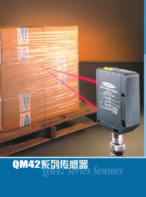
•Email: sensors@327美国邦纳工程国际有限公司QM42 传感器QM42系列QM42系列对射式发射器(E)和接收器(R)红外光,880nm型号检测距离接线方式工作电压输出形式过量增益光形图1101001 m 3.3 ft 10 m 33 ft 100 m 330 ft.1 m .33 ft1000E X C E S S G A I NDISTANCE QM42E/ROpposed Mode 10 m 32.5 ft8 m 26 ft 6 m 19.5 ft 4 m 13 ft 2 m 6.5 ft 0100 mm 200 mm 300 mm100 mm200 mm 300 mm 04 in 8 in 12 in4 in 8 in 12 in DISTANCEQM42E/ROpposed ModeQM426E QM426EQ QM42VN6R QM42VN6RQ QM42VP6R QM42VP6RQ10m (33')10 ~ 30V dc 2m (6.5')电缆4针Euro 接插件2m (6.5')电缆4针Euro 接插件2m (6.5')电缆4针Euro 接插件--互补型NPN 互补型PNP有效光束:8mmQM42带偏振反射板模式可见红光,660nm型号检测距离接线方式工作电压输出形式过量增益光形图1101001 m 3.3 ft 10 m 33 ft 100 m 330 ft.1 m .33 ft1000E X C E S S G A I NDISTANCE QM42LPRetroreflective Mode with BRT-3 Reflector3.75 m 12.5 ft3.0 m 10.0 ft 2.25 m 7.5 ft 1.5 m 5.0 ft 0.75 m 2.5 ft 0020 mm 40 mm 60 mm20 mm00.8 in1.6 in2.4 in0.8 in 40 mm 1.6 in 60 mm 2.4 in DISTANCEQM42LPRetroreflective Modewith BRT-3 ReflectorQM42VN6LP QM42VN6LPQQM42VP6LP QM42VP6LPQ3m (10')10 ~ 30V dc2m (6.5')电缆4针Euro 接插件2m (6.5')电缆4针Euro 接插件互补型NPN互补型PNPPQM42直接反射式红外光,880nm型号检测距离接线方式*工作电压输出形式过量增益光形图11010010 mm .4 in 100 mm 4 in 1000 mm 40 in1 mm .04 in1000E X C E S S G A I NDISTANCEQM42DDiffuse Mode500 mm 20 in400 mm 16 in 300 mm 12 in 200 mm 8 in 100 mm 4 in 0010 mm 20 mm 30 mm10 mm20 mm 30 mm 00.2 in 0.4 in 0.6 in0.4 in 0.8 in 1.2 in DISTANCEQM42DDiffuse ModeQM42VN6D QM42VN6DQ QM42VP6D QM42VP6DQ400mm (16")10 ~ 30V dc2m (6.5')电缆4针Euro 接插件2m (6.5')电缆4针Euro 接插件互补型NPN 互补型PNP短距离长距离短距离1101000.1 m 0.33 ft 1.0 m 3.3 ft 10 m 33 ft0.01 m 0.033 ft1000E X C E S S G A I NDISTANCE QMT42DXDiffuse Mode7.5 m 25 ft6.0 m 20 ft 4.5 m 15 ft 3.0 m 10 ft 1.5 m 5 ft 0010 mm 20 mm 30 mm10 mm20 mm 30 mm 00.4 in 0.8 in 1.2 in0.4 in 0.8 in 1.2 in DISTANCEDiffuse ModeQMT42DXQMT42VN6DXQMT42VN6DXQ QMT42VP6DX QMT42VP6DXQ10mm (0.4")到6m (20")10 ~ 30V dc2m (6.5')电缆4针Euro 接插件2m (6.5')电缆4针Euro 接插件互补型NPN 互补型PNP长距离注意:以上所标注的检测距离是使用反射板BRT-3(3")时的距离,根据所选用的反射板和反光率的大小,实际的检测距离会有所变化。
德国制造的4位数字数字显示压力传感器说明书

1:4-digit alphanumeric display 2:LEDs3:Programming buttonMade inGermanyProduct characteristics Combined pressure sensor ConnectorProcess connection:G 1A /Aseptoflex Vario Display units:bar,psi,MPa,%of the span Function programmable2-wire connection technology:analogue output3-wire connection technology:2outputsOUT1=switching outputOUT2=switching output or analogue output 4-digit alphanumeric displayMeasuring range:-1.00...10.00bar /-14.5...145.0psi /-0.100...1.000MPa Application Type of pressure:relative pressureHygienic systems,viscous media and liquids with suspended particlesLiquids and gasesApplication5MPa 725psi 50bar Pressure rating 15MPa 2175psi 150bar Bursting pressure min.5MPa725psi50barMAWP (for applications according to CRN)-25...125(145max.1h)Medium temperature [°C]Electrical data 2wires DC /3wires DC PNP/NPNElectrical design 20...32DC (2L)/18...32DC (3L)Operating voltage [V] 3.6...21(2L)/<45(3L)Current consumption [mA]>100(500V DC)Insulation resistance[MΩ]III Protection classyesReverse polarity protection Outputs 2-wire connection technology:analogue output3-wire connection technology:2outputsOUT1=switching outputOUT2=switching output or analogue outputOutput1x normally open /normally closed programmable +1x normally open /normallyclosed programmable or 1x analogue (4...20/20...4mA,scalable)Output function ---(2L)/250(3L)Current rating [mA]---(2L)/<2(3L)Voltage drop[V]pulsed Short-circuit protection yesOverload protection ---(2L)/125(3L)Switching frequency [Hz]I:4...20mA (Ineg:20...4mA)Analogue output 300(2L)/max.(Ub -10V)x 50(3L)Max.load[Ω]Measuring /setting range -0.100...1.000MPa -14.5...145.0psi -1.00...10.00bar Measuring range Setting range -0.098...1.000MPa -14.2...145.0psi -0.98...10.00bar Set point,SP -0.100...0.998MPa -14.5...144.7psi -1.00...9.98bar Reset point,rP-0.100...0.750MPa -14.5...108.7psi -1.00...7.50bar Analogue start point,ASP 0.150...1.000MPa21.8...145.0psi1.50...10.00barAnalogue end point,AEP 0.001MPa0.1psi0.01barin steps of SP1=2.50bar;rP1=2.30bar SP2=7.50bar;rP2=7.30bar ASP =0.00bar;AEP =10.00barFactory settingAccuracy /deviations Accuracy /deviations(in %of the span)Turn down 1:1<±0.2Switch point accuracy <±0.2Characteristics deviation *)<±0.15Linearity <±0.15Hysteresis <±0.1Repeatability **)<±0.1Long-term stability ***)Temperature coefficients (TEMPCO)in the temperature range 0...70°C (in %of the span per 10K)<±0.05Greatest TEMPCO of the zero point <±0.15Greatest TEMPCO of the span Reaction times 1(2L)/0.5(3L)Power-on delay time [s]---(2L)/3(3L)Min.response time switching output[ms]0.00...30.00Damping for the switching output (dAP)[s]0.01...99.99Damping for the analogue output (dAA)[s]45(2L)/7(3L)Step response time analogue output[ms]yesIntegrated watchdog Interfaces IO-Link Device COM2(38.4kBaud)Transfer type 1.0IO-Link revision 157d /00009D hIO-Link Device ID no profile Profiles yes SIO modeA Required master port type 1Process data analogue 2Process data binary 2.3Min.process cycle time [ms]Environment -25...80Ambient temperature [°C]-40...100Storage temperature [°C]IP 67/IP 68/IP 69KProtection Tests /approvals EMCDIN EN 61000-6-2DIN EN 61000-6-3Shock resistance 50g (11ms)DIN EN 60068-2-27:Vibration resistance 20g (10...2000Hz)DIN EN 60068-2-6:160MTTF[Years]Mechanical data G 1A /Aseptoflex VarioProcess connection ceramics (99.9%Al2O3);PTFE;stainless steel 316L /1.4435;surfacecharacteristics:Ra <0.4/Rz 4Materials (wetted parts)stainless steel 316L /1.4404;FPM;PTFE;PBT;PEI;PFAHousing materials 100million Switching cycles min.0.313Weight[kg]Displays /operating elements DisplayLED green Display unit LED yellowSwitching status 4-digit alphanumeric display Function display 4-digit alphanumeric displayMeasured values Electrical connection M12connector;Gold-plated contactsConnection Wiring1connection for2-wire operation2connection for3-wire operation3connection for IO-Link parameter setting(P=communication via IO-Link)RemarksRemarks(2L)=value for2-wire operation(3L)=value for3-wire operation*)linearity,incl.hysteresis and repeatability;(limit value setting to DIN16086)**)with temperature fluctuations<10K***)in%of the span per year1Pack quantity[piece]ifm electronic gmbh•Friedrichstraße1•45128Essen—We reserve the right to make technical alterations without prior notice.—GB—PI2794—16.04.2013。
P+F倍加福NJ2-V3-N传感器

P+F倍加福NJ2-V3-N传感器P+F倍加福NJ2-V3-N传感器上海库存P+F倍加福NJ2-V3-N传感器的特点一、灵敏度较高;二、几何形状具有多方面的适应性,可以制成任意形状的光纤传感器;三、可以制造传感各种不同物理信息(声、磁、温度、旋转等)的器件;四、可以用于高压、电气噪声、高温、腐蚀、或其它的恶劣环境;五、而且具有与光纤遥测技术的内在相容性。
P+F倍加福NJ2-V3-N传感器工作原理,可分为物理传感器和化学传感器二大类传感工作原理的分类物理传感器应用的是物理效应,诸如压电效应,磁数伸结现象,离化、极化、热电、光电、磁电等效应。
被测信号量的微小变化都将转换成电信号化学传感器包括那些以化学吸附、电化学反应等现象为因果关系的传感器,被测信号量的微小变化也将转换成电信号有些传感器既不能划分到物理类,也不能划分为化学类。
大多数传感器是以物理原理为基础运作的。
化学传感器技术问题较多,例如可靠性问题,规模生产的可能性,价格间题等,解决了这类难题,化学传感器的应用将会有巨大增长常见传感器的应用领域和工作原理。
P+F倍加福NJ2-V3-N传感器是一种将被测对象的状态转变为可测的光信号的传感器。
光纤传感器的工作原理是将光源入射的光束经由光纤送入调制器,在调制器内与外界被测参数的相互作用,使光的光学性质如光的强度、波长、频率、相位、偏振态等发生变化,成为被调制的光信号,再经过光纤送入光电器件、经解调器后获得被测参数。
整个过程中,光束经由光纤导入,通过调制器后再射出,其中光纤的作用首先是传输光束,其次是起到光调制器的作用。
上海维特锐专业从事各种国外工控自动化产品的进口贸易。
主要经营品牌如下:德国品牌:费斯托FESTO、贺德克HYDAC、宝德BURKERT、力士乐REXROTH、DUNGS 冬斯、霍科德Kromschroeder、曼肯贝格 Mankenberg、S+B、菲尼克斯PHOENIX、施克SICK、皮尔兹PILZ、易福门IFM、恩德斯豪斯E+H、倍加福P+F、巴鲁夫BALLUFF、穆尔MURR、图尔克TURCK、魏德米勒WEIDMULLER、威卡WIKA、亨士乐HENGSTLER、英飞凌/欧派克INFINEON、久茂JUMO、德国德森克/德硕瑞di-soric、德国杰斯曼GESSMANN、德国KUBLER库伯勒、穆勒MOLLER、施迈赛Schmersal、德国EBM、德国雷沃姆RHEWUM、萨姆森SAMSON、EMG伺服阀 GSR、赫斯曼HIRSCHMAN、HBM、 EUCHNER 安士能、DENISON丹尼逊、Bernstein博恩斯坦、ATP泵等。
赛米控丹佛斯电子 SEMiX603GB12E4Ip 数据表
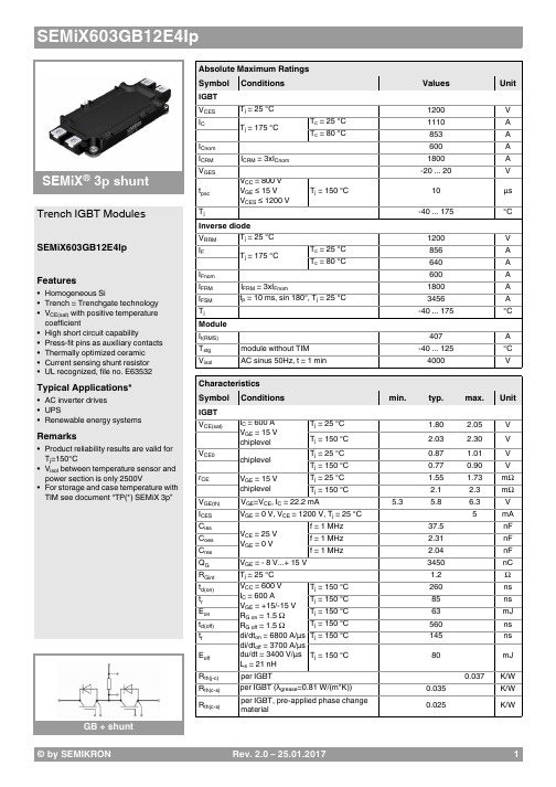
Rev. 2.0–25.01.20171SEMiX ®3p shuntGB + shuntTrench IGBT ModulesSEMiX603GB12E4Ip Features•Homogeneous Si•Trench = Trenchgate technology •V CE(sat) with positive temperature coefficient•High short circuit capability•Press-fit pins as auxiliary contacts •Thermally optimized ceramic •Current sensing shunt resistor •UL recognized, file no. E63532Typical Applications*•AC inverter drives •UPS•Renewable energy systemsRemarks•Product reliability results are valid for T j =150°C•V isol between temperature sensor and power section is only 2500V•For storage and case temperature with TIM see document “TP(*) SEMiX 3p”Absolute Maximum Ratings SymbolConditions Values UnitIGBT V CES T j =25°C 1200V I C T j =175°CT c =25°C 1110A T c =80°C853A I Cnom 600A I CRMI CRM = 3xI Cnom 1800A V GES -20 (20)V t psc V CC =800V V GE ≤ 15V V CES ≤ 1200V T j =150°C10µs T j -40...175°C Inverse diodeV RRM T j =25°C 1200V I F T j =175°CT c =25°C 856A T c =80°C640A I Fnom 600A I FRM I FRM = 3xI Fnom1800A I FSM t p =10ms, sin 180°, T j =25°C3456A T j -40...175°C Module I t(RMS)407A T stg module without TIM -40...125°C V isolAC sinus 50Hz, t =1min4000VCharacteristics SymbolConditionsmin.typ.max.UnitIGBT V CE(sat)I C =600A V GE =15V chiplevel T j =25°C 1.80 2.05V T j =150°C 2.03 2.30V V CE0chiplevel T j =25°C 0.87 1.01V T j =150°C 0.770.90V r CE V GE =15V chiplevelT j =25°C 1.55 1.73m ΩT j =150°C2.12.3m ΩV GE(th)V GE =V CE , I C =22.2mA5.3 5.86.3V I CES V GE =0V,V CE =1200V, T j =25°C 5mA C ies V CE =25V V GE =0Vf =1MHz 37.5nF C oes f =1MHz 2.31nF C res f =1MHz2.04nF Q G V GE =- 8 V...+ 15 V 3450nC R Gint T j =25°C 1.2Ωt d(on)V CC =600V I C =600AV GE =+15/-15V R G on =1.5ΩR G off =1.5Ωdi/dt on =6800A/µs di/dt off =3700A/µs du/dt =3400V/µs L s =21nH T j =150°C 260ns t r T j =150°C 85ns E on T j =150°C 63mJ t d(off)T j =150°C 560ns t f T j =150°C 145ns E off T j =150°C 80mJR th(j-c)per IGBT0.037K/W R th(c-s)per IGBT (λgrease =0.81 W/(m*K))0.035K/W R th(c-s)per IGBT, pre-applied phase change material0.025K/W2Rev. 2.0–25.01.2017© by SEMIKRONSEMiX ®3p shuntGB + shuntTrench IGBT ModulesSEMiX603GB12E4Ip Features•Homogeneous Si•Trench = Trenchgate technology •V CE(sat) with positive temperature coefficient•High short circuit capability•Press-fit pins as auxiliary contacts •Thermally optimized ceramic •Current sensing shunt resistor •UL recognized, file no. E63532Typical Applications*•AC inverter drives •UPS•Renewable energy systemsRemarks•Product reliability results are valid for T j =150°C•V isol between temperature sensor and power section is only 2500V•For storage and case temperature with TIM see document “TP(*) SEMiX 3p”Characteristics SymbolConditionsmin.typ.max.UnitInverse diodeV F = V EC I F =600AV GE =0V chiplevelT j =25°C 2.08 2.44V T j =150°C 2.08 2.34V V F0chiplevel T j =25°C 1.39 1.59V T j =150°C 1.08 1.18V r FchiplevelT j =25°C 1.16 1.42m ΩT j =150°C1.67 1.93m ΩI RRM I F =600A di/dt off =6500A/µs V GE =-15VV CC =600VT j =150°C 465A Q rr T j=150°C108µC E rr T j =150°C 40mJR th(j-c)per diode0.065K/W R th(c-s)per diode (λgrease =0.81 W/(m*K))0.039K/W R th(c-s)per diode, pre-applied phase change material0.031K/W Module L CE 20nH R CC'+EE'measured per switch, shuntexcludedT C =25°C 1.2m ΩT C =125°C 1.65m ΩRth (c-s)1calculated without thermal coupling 0.009K/W Rth (c-s)2including thermal coupling,Ts underneath module (λgrease =0.81 W/(m*K))0.015K/W Rth (c-s)2including thermal coupling,Ts underneath module, pre-applied phase change material 0.011K/W M s to heat sink (M5)36Nm M t to terminals (M6)36Nm Nm w350g Temperature Sensor R 100T c =100°C (R 25=5 k Ω)493 ± 5%ΩB 100/125R (T)=R 100exp[B 100/125(1/T-1/T 100)]; T[K];3550 ±2%KCharacteristics SymbolConditionsmin.typ.max.UnitShunt I Shunt T c =100°C, T Shunt,max =170°C, R th =2.3K/W407A R Shunt Tolerance = ±5 %0.19m Ωα75ppm/K© by SEMIKRON Rev. 2.0–25.01.201734Rev. 2.0–25.01.2017© by SEMIKRONSEMiX 3p shuntpinoutRev. 2.0–25.01.20175This is an electrostatic discharge sensitive device (ESDS), international standard IEC 60747-1, chapter IX.*IMPORTANT INFORMATION AND WARNINGSThe specifications of SEMIKRON products may not be considered as guarantee or assurance of product characteristics ("Beschaffenheitsgarantie"). The specifications of SEMIKRON products describe only the usual characteristics of products to be expected in typical applications, which may still vary depending on the specific application. Therefore, products must be tested for the respective application in advance. Application adjustments may be necessary. The user of SEMIKRON products is responsible for the safety of their applications embedding SEMIKRON products and must take adequate safety measures to prevent the applications from causing a physical injury, fire or other problem if any of SEMIKRON products become faulty. The user is responsible to make sure that the application design is compliant with all applicable laws, regulations, norms and standards. Except as otherwise explicitly approved by SEMIKRON in a written document signed by authorized representatives of SEMIKRON, SEMIKRON products may not be used in any applications where a failure of the product or any consequences of the use thereof can reasonably be expected to result in personal injury. No representation or warranty is given and no liability is assumed with respect to the accuracy, completeness and/or use of any information herein, including without limitation, warranties of non-infringement of intellectual property rights of any third party. SEMIKRON does not assume any liability arising out of the applications or use of any product; neither does it convey any license under its patent rights, copyrights, trade secrets or other intellectual property rights, nor the rights of others. SEMIKRON makes no representation or warranty of non-infringement or alleged non-infringement of intellectual property rights of any third party which may arise from applications. Due to technical requirements our products may contain dangerous substances. For information on the types in question please contact the nearest SEMIKRON sales office. This document supersedes and replaces all information previously supplied and may be superseded by updates. SEMIKRON reserves the right to make changes.6。