ADL5602ARKZ中文资料
Moxa MPC-2150系列15英寸面板计算机说明书

P/N: 1802021500010 *1802021500010*MPC-2150 SeriesQuick Installation GuideEdition 1.0, October 2015Technical Support Contact Information/supportMoxa Americas:Toll-free: 1-888-669-2872 Tel: 1-714-528-6777 Fax: 1-714-528-6778 Moxa China (Shanghai office): Toll-free: 800-820-5036 Tel: +86-21-5258-9955 Fax: +86-21-5258-5505 Moxa Europe:Tel: +49-89-3 70 03 99-0 Fax: +49-89-3 70 03 99-99 Moxa Asia-Pacific:Tel: +886-2-8919-1230 Fax: +886-2-8919-1231 Moxa India:Tel: +91-80-4172-9088 Fax: +91-80-4132-10452015 Moxa Inc. All rights reserved.OverviewThe MPC-2150, 15-inch panel computer, with 3rd generation Intel® Core™ processor delivers a reliable, durable, high-performance platform of wide versatility of use in industrial environments.The MPC-2150 series panel computers are designed with a wide -40 to 70°C temperature range, and come with a patented fanless, streamlined housing designed for highly efficient heat dissipation, making this computer one of most reliable industrial platforms available for harsh, hot, outdoor environments, such as are found at oil and gas fields and on drilling platforms.The MPC-2150 also features a 1,000-nit LCD panel with a sunlight readable and projected capacitive glove-friendly multi-touch screen, providing an excellent user experience for outdoor applications. Package ChecklistBefore installing the MPC-2150, verify that the package contains the following items:•MPC-2150 panel computer• 1 2-pin terminal block for DC power input•SSD/HDD installation kit•Documentation and driver DVD•Quick installation guide (printed)•Warranty cardNOTE: Please notify your sales representative if any of the above items are missing or damaged.Hardware InstallationFront ViewBottom ViewSavvyTouch Display Control ButtonsThe following table describes the SavvyTouch display controls on the front surface of the MPC-2150. These intelligent controls will light up with a simple hand-wave above the area of the screen where they are located.Connector DescriptionAC/DC Power InputThe MPC-2150 allows using either an AC or DC power input. When using AC power, use the standard C14 AC inlet. When using DC power, use at least a 60 W power adapter through the 2-pin terminal block in the accessories package. The figure shows the MPC-2150’s DC pin assignments.Extending the DisplayThe MPC-2150 comes with both standard VGA (DB15) and DVI-D (DB29) interfaces (located on the bottom of the shell) which may be used to simultaneously extend the display across two monitors. Connecting to a Keyboard and Mouse The MPC-2150 Series comes with two PS/2 connectors located on the bottom surface, for connecting a keyboard and a mouse.Serial PortsThe MPC-2150 offers two software-selectable RS-232/422/485 serial ports over a DB9 connector. Refer to the MPC-2150 User’s Manual for serial port configuration details. The pin assignments for the ports are shown in the table below:Ethernet PortsThe pin assignments for the two Fast Ethernet 100/1000 Mbps RJ45 ports are shown in the following table:Refer to the following table for a description of the LAN indicators: LAN(on connectors) Green 100 Mbps Ethernet modeYellow 1000 Mbps (Gigabit) Ethernet mode OffNo activity / 10 Mbps Ethernet modeAudio InterfaceThe MPC-2150 comes with line-in and line-out audio jacks, allowing users to connect a speaker system, an earphone, or a microphone.USB PortsFour USB 2.0 ports are available on the bottom surface. Use these ports to connect mass storage drives and other peripherals.Installing a SATA HDD or SSDThe MPC-2150 comes with an HDD/SSD installation kit accessory. To install the 2.5-inch SATA storage, follow these instructions. For better system reliability, we suggest using a solid state disk (SSD). A list of compatible SSD models is available on Moxa’s website.e 4 screws to fasten the HDD/SSD to the HDD/SSD bracket.2.Remove the 2 screws holding the HDD/SSD cover to the MPC-2150.3.Insert the HDD/SSD (with the bracket) into the HDD/SDD slot. Notedthat the latch on HDD/SSD bracket should be released when pushing the HDD/SSD into the slot.4.Reattach the HDD/SSD cover and fix it to the front panel with the 2screws.Installing a CFast CardThe MPC-2150 has a CFast slot that can be used to install a standard CFast card using a push-push mechanism. A list of compatible CFast cards can be found on Moxa’s website.1. Loosen the screws connecting the HDD/SSD cover to the MPC-2150.2. Insert the CFast card into the slot using the push-push mechanism.3. Reattach the CFast cover. Real Time ClockThe real time clock (RTC) is powered by a lithium battery. We strongly recommend that you do not replace the lithium battery without help from a qualified Moxa support engineer. If you need to change the battery, contact the Moxa RMA service team at/rma/about_rma.aspx .Powering on/off the MPC-2150To power on the panel computer you may either connect power by connecting the Terminal Block to Power Jack Converter to theterminal block and then connect a power adapter, or you may connect the computer to an AC power source using the power cord. After the power source is connected, touch the Menu button to turn the computer on. It takes about 10 to 30 seconds for the system to boot up.To power off the MPC-2150 Series, touch the MENUbutton for 4 seconds; depending on your OS’s power management settings you may enter standby , hibernation , or system shutdown mode. If you encounter technical problems, touch and hold the MENU button for 10 seconds to force a hard shutdown of the system. Grounding the MPC-2150 SeriesProper grounding and wire routing help to limit the effects of noise from electromagnetic interference (EMI). Run the ground connection from the ground screw to the grounding surface prior to connecting the power source.。
奥林匹亚瓷砖产品说明书:海马耳系列

HIMALAYA SeriesPORCELAINAll items shown in this document are part of Olympia’s stocking program. For special orders, please contact yourOlympia Tile Sales Representative.60 x 60 cm (24 x 24) Polished OV.HY.WHT.2424.PL 60 x 60 cm (24 x 24) Polished OV.HY.GRY.2424.PL 60 x 60 cm (24 x 24) PolishedOV.HY.DGR.2424.PL60 x 60 cm (24 x 24) Polished OV.HY.LGR.2424.PLHimalaya Series - Coloured Base Porcelain (Rectified)GREY DARK GREYWHITELIGHT GREYTechnical data is supplied by the manufacturer and is subject to change at any time. Olympia does not provide warranties as to thespecifications of any product.Water AbsorptionISO 10545-3< 0.5%Conforms Bending / Breaking Strength ISO 10545-4>1300N Conforms Modulus of Rupture ISO 10545-4>35 N/mm²Conforms Scratch Hardness MOHs Scale MOHs 5Conforms Chemical Resistance ISO 10545-13min. UB Conforms Frost Resistance ISO 10545-12Required Conforms Stain ResistanceISO 10545-14> Class 3ConformsHIMALAYA SERIESTests Performed -- Results Conform24” x 24”415.5071.6436Packing DetailsExamples of Recommended ApplicationsResidential CommercialIndoorWallFloorColour VariationMemberMember of Canada Green BuildingCouncilMember of U.S. Green BuildingCouncilFor information concerning LEED, please contact our Sales RepresentativeDistributors of America (CTDA)Marble Institute of AmericaOutdoorSEALING INFORMATIONPolished Porcelain should be SEALED WITH A PENETRATING SEALER before grouting. We stock a wide range of high quality sealers. For more specific information please contact one of our sales representatives.Flextile Ltd.INSTALLATION SOLUTIONS SINCE 1946SURFACE PREPARATION (If Required)• Floor levelling: 59 Flex Flo / 5900 Flex Flo Plus Self Levelling Underlayment• Waterproofing: WP900 Waterproof Membrane• Crack Isolation/Uncoupling: Flexilastic 1000 Crack Isolation Membrane / FlexMat Uncoupling Membrane* For a complete listing of FLEXTILE products and accessories including Sound Control, In‐Floor Heating, and further setting options, please visit TaskGrout Sealing¹⸱MORE™ Grout, Ceramic &Porcelain Sealer Ready to useCommercial: 1-3 YearsResidential: 5-8 YearsDaily Maintenance MORE™ Stone and TileCleaner 1 : 128 Ratio DailyDeep Cleaning MORE™ Alkaline Cleaner 1 : 4 Ratio As Needed Grout Haze- Cementitious MORE™ Acidic Cleaner 1 : 4 Ratio As NeededGrout Haze -Epoxy / Urethane MORE™ Coating Stripper*Ready to use As Needed* Always test in an inconspicuous area to make sure the product is achieving the desired results and is not damaging the finish of the surface.1. It is recommended to seal polished porcelains with a penetrating sealer prior to grouting. Please see our selection of MORE Surface Care Products.WHITELIGHT GREYGREYIt is Olympia Tile’s policy to stock all items for sale. Should you require additional sizes, finishes or colours, Olympia has a Special Order Department to help find exactly what you are looking for. Please contact your Olympia Tile Sales Representative for more details. Note that minimum order quantities and longer lead times apply to all special order items.Colour may vary slightly from images shown. It is highly recommended to view physical samples of tile prior to purchase. Note that shade variations between tiles is characteristic and adds to the inherent beauty of the product. Please visit a showroom near you or request a sample from your Olympia Tile Sales Representative.HIMALAYA SERIES: Board MEF-115/ Folder FL-721。
阿尔法拉瓦尔PureSOx 2系列SOx排除器商品说明说明书

Your proven route to competitive SOx complianceSOx scrubbers are the smart choice for complyingwith the global sulphur cap as well as sulphurlimits in Emission Control Areas (ECAs). Alfa LavalPureSOx is the smartest choice of all, because itoffers a complete platform for meeting the needsof your vessel.A route well travelledNo choice of SOx scrubber is more secure than PureSOx,a solution built with Alfa Laval core expertise and decades of marine scrubber experience. PureSOx has been at sea since 2009, reliably cleaning main and auxiliary engine exhaust gas to compliant SOx levels. Today PureSOx has morereferences than any other singleSOx scrubber technology.Among those references arerepeat orders from majorcustomers, as well as a widerange of vessel types andspecifi c scrubber confi gurations.Five reasons to chooseAlfa Laval PureSOx:• Returning customers expresstheir satisfaction• Custom engineering matchesyour vessel and needs• Core technology fromAlfa Laval ensures results• Project management meanstimely delivery and installation• Global service keeps yousecure wherever you sail23The choice of supplierSwitch to low-sulphur fuelMARPOL Annex VIInstall a scrubberAlfa Laval PureSOxSwitch to LNGOther global supplier solutionLocal supplier solutionThe commercial decision The ability to use economical HFO, rather than expensive low-sulphur fuel, rapidly makes a difference in operating costs. Choosing the scrubber route gives you a long-term cost advantage, without making your business dependent on an uncertain LNG infrastructure.The choice of supplierScrubbers are simple in principle, but challenging to adapt for marine use. Although global suppliers have many resources and broader support than local suppliers, their experience should still be reviewed. A long and comprehensive reference list is the best proof that a system can operate successfully in a range of conditions.Alfa Laval PureSOxNot only is Alfa Laval the leading SOx scrubber supplier, the PureSOx platform is also the most complete solution on the market. Your scrubber’s confi guration can be perfectly adapted to the needs of your vessel, no matter where you sail.Mapping your choices Your decisions on the way to SOx compliance can leave you stranded – or put you on the route to success.The PureSOx platform4For all the questions about SOx compliance, there’s ananswer trusted by more and more ship owners. Theunique fl exibility of the PureSOx platform – combinedwith Alfa Laval’s proven expertise – is your assuranceof a compliant and optimized solution.Whatever your PureSOxconfi guration, the results arethe same:• Sulphur removal rate >98%(exceeds IMO requirements)• Particulate matter (PM)trapping up to 80%• Compliance at anyengine loadMany routes to performanceScrubber designTechnology Compliance profileConfigurationArrangement5The PureSOx platform issuccessful because it builds on Alfa Laval core expertise. For over 40 years, Alfa Laval has delivered marine scrubbers as a part of inert gas systems for oil, chemical and LNG carriers.Still more of our expertise is used in closed-loop and hybrid confi gurations. We pioneered centrifugal separation, which is the only reliable means ofcleaning circulation water at sea. The PureSOx water cleaning unit removes particles effectively in all conditions, which minimizes sludge and allows instant bleed-off of cleaned circulation water.As a complete scrubber platform, PureSOx offers three compliance profi les to fi t your specifi c sailing profi le. All versions can be confi gured as open-loop, closed-loop or hybrid arrangements, and as U-design or inline I -design scrubbers.PureSOx GlobalOptimized for use on the open seas, PureSOx Global offers an ideal solution for compliance with the 0.5%S global cap. It is the smallest version of the platform and also provides the greatest ease of installation.PureSOx ECAVessels that spend most or all of their time in Emission Control Ar-eas (ECAs) can meet the more stringent 0.1%S emission limits with PureSOx ECA.This option is also designed to handle the tech-nical restrictions these vessels face, such as low-alkalinity water.PureSOx FlexPureSOx Flex provides an easy switch between 0.5%S and 0.1%S compliance modes. For vessels with more varied operat-ing profi les, this option ensures maximum savings and the lowest possible OPEX.Compliance anywhereBuilt for the way you sail6PureSOx can be confi gured in three different operating arrangements. Which one is right for you depends on where and how your vessel sails.Open-loop arrangement In an open-loop arrangement seawater is used to scrub the exhaust gas, after which it is legally discharged back into the sea. Though the investment and operating costs are lower, the scrubber’s use may be limited by low water alkalinity or local legislation.Closed-loop arrangement In a closed-loop arrangement the scrubber water is dosed with an alkaline additive and recircu-lated. As it becomes dirty, the circulation water is cleaned, dis-charged and replenished to retain capacity . The scrubber can be used anywhere and at any time, but has higher operating costs.Hybrid arrangementA hybrid arrangement is often the perfect compromise, as it provides both open-loop and closed-loop modes. Open-loop operation reduces costs whenever possible, but a switch to closed-loop operation can be made whenever demanded.Open-loop Closed-loop HybridDesigned for your vessel7U-designIn most cases the PureSOx scrubber is confi gured with a U-design. Suitable for the majority of vessels, this confi guration offers a number of advantages. For example, the shape of the scrubber itself forms a natural water trap, preventing water backfl ow to the enginewithout any additional equipment. I-designOn vessels with more complex structural needs, such as certain cruise ships and RoPax vessels, PureSOx can be confi gured with an inline I-design. In this confi guration, water backfl ow is prevented by an internal water trap combined with overboard arrangements.Choosing an I-design can overcome more diffi cult space and stability issues.Inlets for multiple exhaust gas sourcesBoth U-design and I-design scrubbers can be confi gured with multiple inlets. This allows one PureSOx scrubber to clean exhaust gas from both main and auxiliary engines, as well as boil-er exhaust gas.Multiple inlets greatly reduce the footprint and weight of the scrubber system overall, along with the cost of the equipmentand installation.I-designU-design8“We are very satisfi ed in our dealings with Alfa Laval, in terms of both project execution and the technical performance of the PureSOx scrubber. The systems already delivered have all received class approval, and we expect equivalent results from the deliveries in progress.”Emanuele Grimaldi, Managing Director, Grimaldi GroupNothing says more about a scrubber than its references, and repeat orders are the best seal of approval available.Alfa Laval PureSOx has more references than any other single SOx scrubber technology, many of which are repeat orders. All PureSOx systems ever installed are still in compliant operation today.Finnlines and ACL RoRo’s and ConRo’s for Grimaldi Group• Five open-loop PureSOx systems with U-design and multiple inlets • Five hybrid PureSOx systems with U-design and single inletsHow a SOx scrubber and its supplier perform in reality is more important than any specifi cation. Alfa Laval and PureSOx have a solid record of success, not only on board but in the whole process of getting there.PureSOx in practiceReturning customers9“The PureSOx solution was well engineered and allowed a sophisticated integration of the scrubber system into our container feeder ships. The custom construction let us avoid major modifications inside the vessel, which together with the pre-outfitting gave us a short installation time. All those factors contributed to a competitive price.”Christoph Meier, Project Manager, Buss Shipping“[Our vessels’] area of operations will require a closed-loop mode with reliable water cleaning. This is where Alfa Laval’s separation expertise comes into play.”Kevin Douglas, Vice President, Technical Projects andNewbuild, RCLT o be a lasting solution, your scrubber must be engineered to suit your vessel and sailing profile. The PureSOx platform provides a high degree of system flexibility, with multiple operating arrangements, a choice of scrubber designs and many other options.These possibilities allow almost any challenge to be overcome, even on vessels with space and stability issues.It takes considerable knowledge to optimize a scrubber,especially in a closed-loop or hybrid system where compliant cleaning of the circulation water is needed.Alfa Laval has over 40 years of experience with scrubbers spe-cifically, as well as over a century of experience with centrifugal separation – the most reliable method of water cleaning.Custom engineeringCore technology10“Alfa Laval has made things easier in our work with EXMAR so far, and we anticipate that will continue as the EXMAR projects progress. We expect a lot from Alfa Laval as an experienced marine supplier, and when it comes to the professional level of support regarding PureSOx and exhaust gas cleaning, the company delivers.”Lee Dong-hoon, Senior Manager, Hanjin Heavy Industries & Construction (HHIC-TMS)See multimedia content and additional references at /puresoxPureSOx in practiceA solid delivery track record and a structured method of preparing scrubber installations offer insurance against expensive delays and difficulties in class approval.Alfa Laval has not only many years of experience and a strong delivery infrastructure, but also well-documented procedures and clear project management that facilitate class approvals.Project management11”We’ve been extremely pleased with the cooperation with Alfa Laval. DFDS’s policy is that we will never ever bring us in a situation where we can’t comply with the legislation.”Kasper Moos, Vice President T echnical Org., DFDS SeawaysYour scrubber will be with your vessel for many years and will also affect its resale value. This makes it important to choose a stable supplier with a strong global network, who can offer assistance wherever your vessel sails.Alfa Laval has served the marine industry for a century, providing service and support both worldwide and 24/7. The Alfa Laval 360° Service Portfolio offers all the services you need to ensure top performance, uptime and operating efficiency from your PureSOx system throughout its life cycle. You gain easy access to cost-saving insights, high-quality spares and much more.An Alfa Laval Performance Agreement lets you tailor a service plan to your needs. It ensures optimized performance and operating costs for total peace of mind.DFDS RoRo and RoPax vessels• Four hybrid PureSOx systems with U-design and multiple inlets• Nine hybrid PureSOx systems with U-design and single inletsGlobal serviceAlfa Laval in briefAlfa Laval is a leading global provider of specialized products and engineered solutions.Our equipment, systems and services are dedicated to helping customers to optimize the performance of their processes. Time and time again.We help our customers to heat, cool, separate and transport products such as oil, water, chemicals, beverages, foodstuffs, starch and pharmaceuticals.Our worldwide organization works closely with customers in almost 100 countries to help them stay ahead.How to contact Alfa LavalUp-to-date Alfa Laval contact details for all countries are always available on our website at A l f a L a v a l a n d P u r e S O x a r e g l o b a l t r a d e m a r k s o w n e d b y A l f a L a v a l C o r p o r a t e AB .MDD00107EN 1611。
瑞萨电子 CXD5602 用户手册说明书

CXD5602 User ManualContentsContents (2)Figure Contents (7)Table Contents (14)1Introduction (40)1.1Introduction (40)1.2Notation (40)1.2.1Notation of numerical value (40)2CXD5602 Outline (42)2.1Introduction (42)2.2Features (42)2.3Block Diagram (45)2.4Architecture Overview (46)2.5CPU Processor (47)2.5.1Application Processor (47)2.5.2System and I/O Processor (47)2.6Memory Mapping (49)2.6.1Memory Map of Each Block (50)2.6.2Main Memory (51)2.6.3System Memory (52)2.6.4Backup Memory (52)2.7Clock and Reset (52)2.7.1Overview (52)2.7.2Clock Architecture (55)2.8Power Management (57)2.8.1Overview (57)2.8.2Power Domain (57)2.8.3Power Supply States (60)3Function Details (62)3.1I/O Configuration (62)3.1.1Outline (62)3.1.2Function List (62)3.1.3Switching between HOST I/F Select Function and SWD Function (63)3.1.4Pin Multiplexer (64)3.2General Purpose Input/Output (GPIO) (95)3.2.1Outlines and Features (95)3.2.2Function List (95)3.2.3Function Specification Outlines (96)3.2.4Detailed Function and Control Specification (98)3.3Interrupt (121)3.3.1Overview and Features (121)3.3.2Register Descriptions (122)3.4PMU (Power Management Unit) (125)3.4.1Features and Overview (125)3.4.2Register List (135)3.4.3Register Descriptions (137)3.4.4Power Supply Control Flow (149)3.4.5Power Supply Control Example (163)3.5Clock and Reset (Clock Reset Generator) (167)3.5.1Overview (167)3.5.2Clock Scheme for CRG (167)3.5.3Analog Circuits (169)3.5.4Clock Setting Confirmation (172)3.5.5Power Domain Reset (175)3.5.6Reset by WDT (176)3.6RTC (179)3.6.1Outlines and Features (179)3.6.2Clock Input (180)3.6.3Function List (181)3.6.4Function Block Diagrams (181)3.6.5Detailed Function and Control Specification (184)3.7I2C (222)3.7.1Overview (222)3.7.2Features (225)3.7.3Functional description (226)3.7.4List of Registers (250)3.8DMAC (278)3.8.1Overview and Features (278)3.8.2Function Descriptions (278)3.8.3SDMAC (280)3.8.4HDMAC (283)3.8.5SYDMAC (285)3.8.6SYSUBDMAC (286)3.8.7ADMAC (287)3.8.8IDMAC (289)3.9SCU (Sensor Control Unit) (301)3.9.1SCU Overview and Features (301)3.9.2SCU Block Diagram (303)3.9.3Memory Map (304)3.9.4Clock Control (307)3.9.5Power Supply Control (313)3.9.6Interrupt (313)3.9.7MATH_PROC processing (318)3.9.8FIFO (328)3.9.9Sequencers (334)3.9.10DMA (356)3.9.11PWM (358)3.9.12SCU Register Details (369)3.9.13SCU Control Sequence (870)3.9.14Error Handling (914)3.9.15Restrictions (915)3.10SPI (930)3.10.1Overview and Features (930)3.10.2SPI0 (932)3.10.3SPI3 (933)3.10.4SPI4 (934)3.10.5SPI5 (936)3.10.6List of Registers (937)3.11UART (949)3.11.1Overview and Features (949)3.11.2UART1 (950)3.11.3UART2 (952)3.11.4List of Registers (953)3.12GNSS (965)3.13APP (967)3.13.1Function Overview (967)3.13.2Power Supply Control (970)3.13.3Clock Reset Control (971)3.13.4Description of APP_DSP Function (982)3.14SYSIOP Clock and Reset Control (1007)3.14.1Function Overiew (1007)3.14.2Power Supply Control (1010)3.14.3Clock and Reset Control (1011)3.15Audio Codec (1029)3.15.1Audio Codec Overview and Features (1029)3.15.2Audio Codec Block Diagram (1030)3.15.3Clock Supply (1035)3.15.4Standalone Operation (without the CXD5247) (1035)3.15.5External Interfaces (1036)3.15.6Details of Audio Codec Control Registers (1038)3.15.7Status Register (1083)3.15.8Interrupt Flag (1087)3.15.9Audio Codec Control Register List (1090)3.15.10Control Sequence (1106)3.16SDIO (1112)3.17eMMC (1112)3.18USB (1112)3.18.1Overview (1113)3.18.2Configuration Parameters (1118)3.18.3Theory of Operation (1124)3.18.4DMA Mode (1124)3.18.5Slave-Only Mode (1128)3.18.6Control and Status Registers (1131)3.18.7Slave-Only Operation (1172)3.18.8DMA Operation (1181)3.18.9Application Bus Protocol (Slave-Only Mode) (1201)3.18.10Application Bus Protocol (DMA Mode) (1203)3.18.11Software Implementation Guidelines (1205)3.18.12USB Programming (1211)3.18.13Multiple RxFIFO Controllers (1233)3.19CIS I/F (1238)3.202D Graphics (1238)3.21ADC (1239)3.21.1ADC Overview (1239)3.21.2ADC Block Diagram (1240)3.21.3Memory Map (1240)3.21.4Power Supply Control (1241)3.21.5Clock Control (1242)3.21.6Reset Control (1245)3.21.7Interrupt (1245)3.21.8FIFO writing Process (1245)3.21.9Gain Control (1246)3.21.10Performance Estimation (1248)3.21.11Synchronization Function with PWM (1249)3.21.12ADC Control Register Details (1249)3.21.13ADC Control Sequence (1285)3.21.14Restrictions (1285)3.21.15Error Handling (1286)4Appendix (1287)4.1Words and Terms (1287)4.1.1Words and Terms Used in This User Manual (1287)4.2Reference (1289)Revision History (1290)Figure ContentsFigure Block Diagram-1 CXD5602 Block Diagram (45)Figure Memory Mapping-2 Memory Map of the SYSIOP, GNSS, and APP (49)Figure Clock and Reset-3 Clock Diagram (56)Figure Power Management-4 Power Domain Layers (57)Figure Power Management-5 CXD5602 Power Domain (58)Figure Power Management-6 Changes of Power Supply States (61)Figure I/O Configuration-7 Switching between HOST I/F Function and SWD Function (63)Figure I/O Configuration-8 Visualized Function inside IOCELL Controlled by IOCELL Control Register (75)Figure I/O Configuration-9 Examples of Assigning Roles to the Pin (P1r_02) (79)Figure I/O Configuration-10 PMIC_INT Signal Routes (MODE=1) (81)Figure I/O Configuration-11 PMIC_INT Signal Routes (MODE=2 Open Drain) (82)Figure I/O Configuration-12 RTC_IRQ_OUT Signal Routes (MODE=2 Open Drain) (83)Figure I/O Configuration-13 SDIO CLK Input Schematic (91)Figure I/O Configuration-14 SDIO WP/CD Input Control Register Schematic (92)Figure General Purpose Input/Output (GPIO)-15 GPIO Overview Block Diagram (96)Figure General Purpose Input/Output (GPIO)-16 Diagram of GPIO Event Detect Block (97)Figure General Purpose Input/Output (GPIO)-17 Output Signal Route in the I/O Function Controlled by GPIO Parameter (100)Figure General Purpose Input/Output (GPIO)-18 Input Signal Route in the I/O Function Controlled by GPIO Parameter (101)Figure General Purpose Input/Output (GPIO)-19 GPIO Pin Selection (102)Figure General Purpose Input/Output (GPIO)-20 External Interrupt Selection (106)Figure General Purpose Input/Output (GPIO)-21 Event Detection Control (109)Figure General Purpose Input/Output (GPIO)-22 Event Detection Timing Diagram (112)Figure General Purpose Input/Output (GPIO)-23 Connection Diagram of Event Detection and SYSCPU or DSP (117)Figure General Purpose Input/Output (GPIO)-24 Time Interval for a Signal to be able to Detect an Event Again (PMU_WAKE_TRIG_NOISECUTEN0:0) (120)Figure Interrupt-25 Interrupt Connection Diagram (121)Figure PMU (Power Management Unit)-26 PMU and the Power Domain Layers (125)Figure PMU (Power Management Unit)-27 Individual Power Supply Control within the Power Domains (127)Figure PMU (Power Management Unit)-28 Power Supply Control within the Power Domain (PWD_APP Main Memory) (128)Figure PMU (Power Management Unit)-29 Changes of Power Supply States (130)Figure PMU (Power Management Unit)-30 Overall Block Diagram of the PMU (133)Figure PMU (Power Management Unit)-31 PMU Clock System (134)Figure PMU (Power Management Unit)-32 Sleep/Wakeup Control Flow of the Application Processor (166)Figure Clock and Reset (Clock Reset Generator)-33 CRG Control Area within Overall Clock Scheme (168)Figure Clock and Reset (Clock Reset Generator)-34 CRG Clock Scheme (168)Figure RTC-35 RTC0/1 Power Supply Framework (179)Figure RTC-36 Clock Resources of RTC (181)Figure RTC-37 RTC Block Diagram (182)Figure RTC-38 RTC (Time Update) Block Diagram (183)Figure I2C-39 I2C0/I2C1 Clock and Reset System (223)Figure I2C-40 I2C2 Clock and Reset System (224)Figure I2C-41 Master/Slave and Transmitter/Receiver Relationships (227)Figure I2C-42 Data transfer on the I2C Bus (228)Figure I2C-43 START and STOP Condition (229)Figure I2C-44 7-bit Address Format (230)Figure I2C-45 10-bit Address Format (230)Figure I2C-46 Master-Transmitter Protocol (231)Figure I2C-47 Master-Receiver Protocol (231)Figure I2C-48 START BYTE Transfer (232)Figure I2C-49 IC_DATA_CMD Register if IC_EMPTYFIFO_HOLD_MASTER_EN = 0 (233)Figure I2C-50 Master Transmitter Tx FIFO Becomes Empty if IC_EMPTYFIFO_HOLD_MASTER_EN=0 (233)Figure I2C-51 Master Receiver Tx FIFO Becomes Empty if IC_EMPTYFIFO_HOLD_MASTER_EN=0 (234)Figure I2C-52 IC_DATA_CMD Register if IC_EMPTYFIFO_HOLD_MASTER_EN = 1 (234)Figure I2C-53 Master Transmitter Tx FIFO Empties/STOP Generation if IC_EMPTYFIFO_HOLD_MASTER_EN=1 (235)Figure I2C-54 Master Receiver Tx FIFO Empties/STOP Generation if IC_EMPTYFIFO_HOLD_MASTER_EN=1 (235)Figure I2C-55 Master Transmitter Restart Bit of IC_DATA_CMD is set (IC_EMPTYFIFO_HOLD_MASTER_EN=1) (236)Figure I2C-56 Master Receiver Restart Bit of IC_DATA_CMD is set (IC_EMPTYFIFO_HOLD_MASTER_EN=1) (236)Figure I2C-57 Master Transmitter Stop Bit of IC_DATA_CMD Set/Tx FIFO Not Empty (IC_EMPTYFIFO_HOLD_MASTER_EN=1) (236)Figure I2C-58 Master Transmitter First Byte Loaded into Tx FIFO Allowed to Empty, Restart Bit Set (IC_EMPTYFIFO_HOLD_MASTER_EN=1) (237)Figure I2C-59 Master Receiver Stop Bit of IC_DATA_CMD Set/Tx FIFO Not Empty (IC_EMPTYFIFO_HOLD_MASTER_EN=1) (237)Figure I2C-60 Master Receiver First Command Loaded After Tx FIFO Allowed to Empty, Restart Bit Set (IC_EMPTYFIFO_HOLD_MASTER_EN=1) (237)Figure I2C-61 Multiple Master Arbitration (238)Figure I2C-62 Multi-Master Clock Synchronization (239)Figure I2C-63 Spike Suppression Example (242)Figure I2C-64 Impact of SCL Rise Time and Fall Time on Generated SCL (244)Figure I2C-65 IC_SDA_HOLD Register (247)Figure I2C-66 IC_SDA_RX_HOLD >= 3 (248)Figure I2C-67 IC_SDA_RX_HOLD = 2 (248)Figure I2C-68 DW_apb_i2c Master Implementing tHD; DAT with IC_SDA_HOLD = 3 (249)Figure DMAC-69 SDMAC Overview of Added Functions (280)Figure DMAC-70 SDMAC Clock and Reset System (282)Figure DMAC-71 HDMAC Overview of Added Functions (283)Figure DMAC-72 HDMAC Clock and Reset System (284)Figure DMAC-73 SYDMAC Clock and Reset System (285)Figure DMAC-74 SYSUBDMAC Clock and Reset System (287)Figure DMAC-75 ADMAC Clock and Reset System (288)Figure DMAC-76 IDMAC Function Block Diagram (289)Figure DMAC-77 IDMAC Clock and Reset System (300)Figure SCU (Sensor Control Unit)-78 Block Function Overview (303)Figure SCU (Sensor Control Unit)-79 Memory Mapping from the Upper CPUs; the CPU in the SYSIOP and the CPU in the GNSS; (hereinafter in the Chapter on SCU, referred as “upper CPUs”) (304)Figure SCU (Sensor Control Unit)-80 Memory Mapping within the SCU as seen from the Upper CPUs (305)Figure SCU (Sensor Control Unit)-81 Memory Mapping as seen from the Internal Sequencer (306)Figure SCU (Sensor Control Unit)-82 Memory Mapping as seen from the HOSTIFC (306)Figure SCU (Sensor Control Unit)-83 Clock System (309)Figure SCU (Sensor Control Unit)-84 Interrupt Connections (314)Figure SCU (Sensor Control Unit)-85 Decimation Partition Data Path (319)Figure SCU (Sensor Control Unit)-86 Normal Sensor Partition Data Path (319)Figure SCU (Sensor Control Unit)-87 Preprocessing Data Flow (320)Figure SCU (Sensor Control Unit)-88 Decimation Processing Data Flow (321)Figure SCU (Sensor Control Unit)-89 Data Flow within the Math Function (322)Figure SCU (Sensor Control Unit)-90 2 2nd Order IIR Filter Combinations (323)Figure SCU (Sensor Control Unit)-91 2nd Order IIR Filter Internal Data Flow (324)Figure SCU (Sensor Control Unit)-92 Normalization Processing Data Flow (324)Figure SCU (Sensor Control Unit)-93 Excess Detection Operation (by a Comparator and an Excess Detector) . 325 Figure SCU (Sensor Control Unit)-94 Excess Detection Operation (Two-step Cascade Connection) (326)Figure SCU (Sensor Control Unit)-95 FIFO Block Diagram (334)Figure SCU (Sensor Control Unit)-96 Sequencer Overall Image (336)Figure SCU (Sensor Control Unit)-97 Sequencer Process Flow (Example) (336)Figure SCU (Sensor Control Unit)-98 Overall Data Flow (excluding Data Duplication Function) (337)Figure SCU (Sensor Control Unit)-99 Startup Control (338)Figure SCU (Sensor Control Unit)-100 External Bus Transaction Generation (339)Figure SCU (Sensor Control Unit)-101 External Data Capture (340)Figure SCU (Sensor Control Unit)-102 Sensor Data Flow when Capturing External Data (341)Figure SCU (Sensor Control Unit)-103 Data Normalization (Example) (342)Figure SCU (Sensor Control Unit)-104 Data Stacked in the FIFO (Image) (343)Figure SCU (Sensor Control Unit)-105 Sequencer Data Flow (350)Figure SCU (Sensor Control Unit)-106 Sequencer Completed (352)Figure SCU (Sensor Control Unit)-107 Sequencer Suspended (352)Figure SCU (Sensor Control Unit)-108 MATH_PROC Parameter Change (Example) (353)Figure SCU (Sensor Control Unit)-109 Error Notification (Example) (355)Figure SCU (Sensor Control Unit)-110 DMA Handshake Signal Connections (357)Figure SCU (Sensor Control Unit)-111 PWM Output Mode using ADC Timing as a Reference (361)Figure SCU (Sensor Control Unit)-112 ADC Data Capture Mode using the PWM Output Timing as a Reference (364)Figure SCU (Sensor Control Unit)-113 Processing Block Overview (412)Figure SCU (Sensor Control Unit)-114 Filter Overview (414)Figure SCU (Sensor Control Unit)-115 Excess Detection Overview (450)Figure SCU (Sensor Control Unit)-116 I2C Master Control (Example) (918)Figure SCU (Sensor Control Unit)-117 Basic Startup Timing (919)Figure SCU (Sensor Control Unit)-118 Delay at Start (Example) (919)Figure SCU (Sensor Control Unit)-119 Time Stamp Fluctuation by the Presence/Absence of HPADC Execution (924)Figure SCU (Sensor Control Unit)-120 Counter Basic Operation (925)Figure SCU (Sensor Control Unit)-121 1 One-to-One Connection (Example) (926)Figure SCU (Sensor Control Unit)-122 One-to-N Connection (Example) (927)Figure SPI-123 SPI0 Clock and Reset System (933)Figure SPI-124 SPI3 Clock and Reset System (934)Figure SPI-125 SPI4 Clock and Reset System (935)Figure SPI-126 SPI5 Clock and Reset System (936)Figure SPI-127 Mode0, single transfer (939)Figure SPI-128 Mode0, continuous transfer (939)Figure SPI-129 Mode1, single and continuous transfers (940)Figure SPI-130 Mode2, single transfer (941)Figure SPI-131 Mode2, continuous transfer (941)Figure SPI-132 Mode3, single and continuous transfers (942)Figure UART-133 UART1 Clock and Reset System (951)Figure UART-134 UART2 Clock and Reset System (952)Figure APP-135 Application Domain Clock System (972)Figure APP-136 Application Domain Reset System (973)Figure APP-137 APP_DSP Block Diagram (983)Figure APP-138 WDTRES Connection (990)Figure APP-139 Address Map (994)Figure APP-140 Input-Output Addresses of Address Converter (995)Figure APP-141 Address Conversion Operation Scheme (996)Figure APP-142 Example of Address Conversion: Conversion of Bit Assignment for ADSP0 (999)Figure APP-143 Example of Address Conversion: Conversion Address Map for ADSP0 and ADSP1 (999)Figure APP-144 Success Case 1 of Exclusive Access (1001)Figure APP-145 Success Case 2 of Exclusive Access (1001)Figure APP-146 Failure Case 1 of Exclusive Access (1002)Figure APP-147 Failure Case 2 of Exclusive Access (1002)Figure APP-148 Failure Case 3 of Exclusive Access (1002)Figure SYSIOP Clock and Reset Control-149 SYSIOP Clock Configuration Diagram (1012)Figure SYSIOP Clock and Reset Control-150 SYSIOP Reset Configuration Diagram (1026)Figure 3.15-1 Audio Codec Block Diagram (1030)Figure 3.15-2 I2S Signal Path (1031)Figure 3.15-3 Mic Signal Path (1032)Figure 3.15-4 SP Signal Path (1034)Figure 3.15-5 Serializer Timing Chart (1035)Figure 3.15-6 I2S Format 24bit (1036)Figure 3.15-7 Left Justified 24bit (1037)Figure 3.15-8 CXD5247 Interface (SP) (MIC) (1037)Figure 3.15-9 DMIC Timing (1038)Figure 3.15-10 Internal Signal Selector Overview Diagram (1040)Figure 3.15-11 Characterstics of the Band Limiting Filter (HI_RES_MODE:1'b1, SRC{1,2}:2'b10) (1053)Figure 3.15-12 Characterstics of the Band Limiting Filter (HI_RES_MODE:1'b1, SRC{1,2}:2'b01) (1054)Figure 3.15-13 Volume Control Overview Diagram (1055)Figure 3.15-14 Example of ALC_TARGET Control (ALC_KNEE:7'h00) (1056)Figure 3.15-15 Example of ALC_KNEE Control (ALC_TARGET:6'h00) (1057)Figure 3.15-16 The HP Output Signal in Normal Mode (fs = 48 kHz) with ALC function OFF and Input Signal Level: -6 dB/-26 dB (1059)Figure 3.15-17 The HP Output Signal in Normal Mode (fs = 48 kHz) with ALC function ON, SPC_ALC_RELEASE = 0x000100, ALC_ALG = 1'b0, and Input Signal Level -6 dB/-26 dB (1059)Figure 3.15-18 The HP Output Signal in Normal Mode (fs = 48 kHz) with SPC function ON, SPC_ALC_ATTACK = 0x000100, and Input Signal Level -6 dB/-26 dB (1060)Figure 3.15-19 AWEIGHT Filter Characteristics (Hi-Res Mode) (1061)Figure 3.15-20 AWEIGHT Filter Chracteristics (Normal Mode) (1061)Figure 3.15-21 Order of Processing DEQ, ALC, and Clear Stereo (HI_RES_MODE:1'b1, ALC_REC:1'b0) (1062)Figure 3.15-22 Order of Processing DEQ, ALC, and Clear Stereo (HI_RES_MODE:1'b1, ALC_REC:1'b1) 1062Figure 3.15-23 Order of Processing DEQ, ALC, and Clear Stereo (HI_RES_MODE:1'b0, ALC_REC:1'b0) (1062)Figure 3.15-24 Order of Processing DEQ, ALC, and Clear Stereo (HI_RES_MODE:1'b0, ALC_REC:1'b1) (1063)Figure 3.15-25 Order of Processing DEQ, SPC, and Clear Stereo (1063)Figure 3.15-26 Decimation Filter Peripheral Overview (1064)Figure 3.15-27 Characteristics of 1/2-band Decimation Filter (1065)Figure 3.15-28 Characteristics of 1/4-band Decimation Filter (1066)Figure 3.15-29 Characteristics of 1/8-band Decimation Filter (1066)Figure 3.15-30 BUS MASTER(MIC) Block (1071)Figure 3.15-31 Bit Configuration by Transfer Mode (when writing to the SRAM) (1072)Figure 3.15-32 BUS MASTER (I2S0/I2S1) Block (1072)Figure 3.15-33 Bit Configuration by Transfer Mode (when writing to the SRAM) (1073)Figure 3.15-34 Bit Configuration by Transfer Mode (when reading from the SRAM) (1073)Figure 3.15-35 Mic Signal Upload Flow (Example) (1108)Figure 3.15-36 I2S0 Signal Upload Flow (Example) (1109)Figure USB-37 UDC-AHB Subsystem Architecture (1114)Figure USB-38 Clock Boundary (1117)Figure USB-39 IN Transaction Flow in DMA Mode (1125)Figure USB-40 OUT Transaction Flow in DMA Mode (Without Thresholding) (1127)Figure USB-41 IN Transaction Flow in Slave-Only Mode (1129)Figure USB-42 OUT Transaction Flow in Slave-Only Mode (1130)Figure USB-43 Memory Map (Processor Viewpoint) (1166)Figure USB-44 UDC-AHB Subsystem Architecture (1173)Figure USB-45 External RAM Write/Read Transfer (1177)Figure USB-46 FIFO Confirm Mechanism (1177)Figure USB-47 RxFIFO Implementation (1179)Figure USB-48 Descriptor Memory Structure (1182)Figure USB-49 SETUP Data Memory Structure (1183)Figure USB-50 OUT Data Memory Structure (1184)Figure USB-51 IN Data Memory Structure (1186)Figure USB-52 Control/Bulk-IN Transaction in Packet-Per-Buffer With Descriptor Update Mode (1192)Figure USB-53 Control/Bulk-IN Transaction in Packet-Per-Buffer Without Descriptor Update Mode (1193)Figure USB-54 OUT Transaction in Packet-Per-Buffer Mode With Descriptor Update (1194)Figure USB-55 OUT Transaction in Packet-Per-Buffer Mode Without Descriptor Update (1195)Figure USB-56 DMA Processing OUT Packets in Buffer Fill Mode (1196)Figure USB-57 DMA Processing OUT Packets in Packet-Per-Buffer With Descriptor Update Mode With Threshold Enabled (1198)Figure USB-58 Byte Ordering (Endianness) Conversion (1199)Figure USB-59 OUT Transaction Flow in DMA Mode Without Thresholding Enabled (1235)Figure USB-60 OUT Transaction Flow in DMA Mode With Thresholding Enabled (1236)Figure USB-61 OUT Transaction Flow in Slave-Only Mode (1237)Figure ADC-62 Block Diagram ADCIF module and around ADC macro circuits (1240)Figure ADC-63 Memory Map inside the ADCIF (1241)Figure ADC-64 Schematic Diagram of the Clock Control (1243)Figure ADC-65 Data Flow of the ADC (1245)Figure ADC-66 HPADC Gain Control Overview (1247)Table ContentsTable Notation-1 Notation of Numerical Value (40)Table Memory Mapping-2 Memory Mapping of the SYSIOP Block (SYS Window) (50)Table Memory Mapping-3 Memory Mapping of the APP Block (APP Window) (51)Table Power Management-4 Power Supply States (60)Table I/O Configuration-5 Function List (62)Table I/O Configuration-6 HOST I/F Decided in Accordance with Pin SYSTEM{0,1} (63)Table I/O Configuration-7 List of Registers for Controlling Pin Multiplexer (64)Table I/O Configuration-8 List of Registers for Controlling IOCELL (64)Table I/O Configuration-9 List of Registers for AUDIO and SDIO Control (67)Table I/O Configuration-10 Overview of Registers for Selecting a Role of the I/O Pins Belonging to SYS Group (68)Table I/O Configuration-11 Table of Role Selection for I/O Pins Belonging to SYS Group (69)Table I/O Configuration-12 Overview of Registers for Selecting a Role of the I/O Pins Belonging to APP Group (71)Table I/O Configuration-13 Table of Role Selection for the I/O Pins Belonging to APP Group (72)Table I/O Configuration-14 Overview of Registers to Select Function of IOCELL (74)Table I/O Configuration-15 Correspondence Table of IOCELL Control Registers and Controllable I/O Pins (76)Table I/O Configuration-16 Overview of Registers for Selecting Output Function of I2S (77)Table I/O Configuration-17 Overview of Register for Selecting PDM_CLK Output Function (77)Table I/O Configuration-18 Overview of Registers for Selecting Input Value to SDIO (78)Table General Purpose Input/Output (GPIO)-19 Function List (95)Table General Purpose Input/Output (GPIO)-20 GPIO Control Register (98)Table General Purpose Input/Output (GPIO)-21 Correspondence of GPIO Control Registers to I/O Pins (99)Table General Purpose Input/Output (GPIO)-22 IO Pin Selection (SYS Group) (103)Table General Purpose Input/Output (GPIO)-23 Correspondence of I/O Pins to Setting Values (SYS Group) (104)Table General Purpose Input/Output (GPIO)-24 I/O Pin Selection (APP Group) (104)Table General Purpose Input/Output (GPIO)-25 Correspondence of I/O Pins to Setting Values (APP Group) (105)Table General Purpose Input/Output (GPIO)-26 External Interrupt Selection (107)Table General Purpose Input/Output (GPIO)-27 I/O Pins That Can be Used for Event Detection (110)Table General Purpose Input/Output (GPIO)-28 Event Detection Setting for I/O Pins (112)Table General Purpose Input/Output (GPIO)-29 Status of Event Detection (115)Table General Purpose Input/Output (GPIO)-30 Registers to Clear the Status of the Event Detections (116)Table General Purpose Input/Output (GPIO)-31 Time Interval for a Signal to be Able to Detect an Event Again (1*) (119)Table Interrupt-32 List of Interrupt Registers of Application Processor (122)Table Interrupt-33 Interrupt Factor Registers of Application Processor (122)Table PMU (Power Management Unit)-34 Power Supply States (129)Table PMU (Power Management Unit)-35 The Setting of the Power Supply in “Reset” State and After Changing to “Normal” State (130)Table PMU (Power Management Unit)-36 PMU Register List (135)Table PMU (Power Management Unit)-37 Power Supply Control Settings (Power Domain) (137)Table PMU (Power Management Unit)-38 Power Supply Status (Power Domain) (138)Table PMU (Power Management Unit)-39 Power Supply Control Settings (SRAM) (139)Table PMU (Power Management Unit)-40 Power Supply Status (SRAM) (141)Table PMU (Power Management Unit)-41 Power Supply Control Settings (Analog Circuit) (143)Table PMU (Power Management Unit)-42 Power Supply Status (Analog Circuit) (144)Table PMU (Power Management Unit)-43 Power Supply Control Request (145)Table PMU (Power Management Unit)-44 Interrupt (145)Table PMU (Power Management Unit)-45 Power Supply Setting Check (146)Table PMU (Power Management Unit)-46 Power Supply Setting Check Items (147)Table PMU (Power Management Unit)-47 Power Supply Control Setting Values (149)Table PMU (Power Management Unit)-48 Parameter Setting for Each Mode (155)Table PMU (Power Management Unit)-49 Current Adjustment Setting (156)Table PMU (Power Management Unit)-50 SYSPLL Division Ratio Setting (158)Table Clock and Reset (Clock Reset Generator)-51 RCOSC Block Status Registers (169)Table Clock and Reset (Clock Reset Generator)-52 XOSC Block Status Register (170)Table Clock and Reset (Clock Reset Generator)-53 SYSPLL Frequency Confirmation (171)Table Clock and Reset (Clock Reset Generator)-54 SYSPLL Block Status Registers (171)Table Clock and Reset (Clock Reset Generator)-55 Clock Switching Status Registers (172)Table Clock and Reset (Clock Reset Generator)-56 Clock Enable Status Registers (174)Table Clock and Reset (Clock Reset Generator)-57 Power Domain and the Reset Control Registers (175)Table Clock and Reset (Clock Reset Generator)-58 Reset Registers of the Power Domain (176)Table Clock and Reset (Clock Reset Generator)-59 WDT Reset Control Registers (177)Table RTC-60Clock Resource of RTC (180)Table RTC-61 Clock Enable of RTC (180)Table RTC-62 Function List (181)Table RTC-63 Register List of Counter Value Write Control System (184)Table RTC-64 Register List of Time Counter Value Read Control System (184)Table RTC-65 Register List of Alarm Control System (185)Table RTC-66 Register List of Time Update Confirming System (186)Table RTC-67 List of External Alarm Output and Time Synchronization Register (186)Table RTC-68 Alarm Occurrence Condition (206)Table RTC-69 Examples of Setting Synchronizing Internal RTC with External RTC Synchronization Setting .. 218Table I2C-70 I2C List (222)Table I2C-71 XOSC (26 MHz), High Performance Mode (225)Table I2C-72 XOSC (26 MHz), Low Power Mode (225)Table I2C-73 IC_CON (252)Table I2C-74 IC_TAR (254)Table I2C-75 IC_SAR (254)Table I2C-76 IC_HS_MADDR (254)Table I2C-77 IC_DATA_CMD (255)Table I2C-78 IC_SS_SCL_HCNT (256)Table I2C-79 IC_SS_SCL_LCNT (256)Table I2C-80 IC_FS_SCL_HCNT (257)Table I2C-81 IC_FS_SCL_LCNT (257)Table I2C-82 IC_HS_SCL_HCNT (258)Table I2C-83 IC_HS_SCL_LCNT (258)Table I2C-84 IC_INTR_STAT (259)Table I2C-85 IC_INTR_MASK (259)Table I2C-86 IC_RAW_INTR_STAT (260)Table I2C-87 IC_RX_TL (262)Table I2C-88 IC_TX_TL (262)Table I2C-89 IC_CLR_INTR (263)Table I2C-90 IC_CLR_RX_UNDER (263)Table I2C-91 IC_CLR_RX_OVER (263)Table I2C-92 IC_CLR_TX_OVER (263)Table I2C-93 IC_CLR_RD_REQ (264)Table I2C-94 IC_CLR_TX_ABRT (264)Table I2C-95 IC_CLR_RX_DONE (264)Table I2C-96 IC_CLR_ACTIVITY (264)Table I2C-97 IC_CLR_STOP_DET (265)Table I2C-98 IC_CLR_START_DET (265)Table I2C-99 IC_CLR_GEN_CALL (265)Table I2C-100 IC_ENABLE (265)Table I2C-101 IC_STATUS (267)Table I2C-102 IC_TXFLR (268)Table I2C-103 IC_RXFLR (268)Table I2C-104 IC_SDA_HOLD (269)Table I2C-105 IC_TX_ABRT_SOURCE (269)Table I2C-106 IC_SLV_DATA_NACK_ONLY (271)Table I2C-107 IC_DMA_CR (271)Table I2C-108 IC_DMA_TDLR (271)。
戴尔Wyse 5000系列瘦客户端Wyse 5060快速入门指南说明书

5060Install the standMonteer de monitorstandaardInstaller le socleAnbringen des Ständers1Connect the keyboard and mouseSluit het toetsenbord en de muis aanConnecter le clavier et la sourisTastatur und Maus anschließen2Connect the power cable andpress the power buttonSluit de stroomkabel aan en druk op de aan-uitknopConnecter le câble d’alimentation et appuyer sur le bouton d’alimentationStromkabel anschließen und Betriebsschalter drücken5Connect the display andpress the power buttonSluit het scherm aan en druk op de aan-uitknopConnectez l’écran et appuyez sur le bouton d’alimentationBildschirm anschließen und Betriebsschalter drücken4Connect the network interfaceSluit de netwerkinterface aanConnecter l’interface réseauNetzwerkschnittstelle anschließen3o remove the SFP interface, rotate the latch and unplug it from its slot.verwijder de SFP-interface door de vergrendeling te draaien en deze uit de sleuf tepour retirer l’interface SFP, faites pivoter le loquet et retirez-le de son logement.Um die SFP-Schnittstelle zu entfernen, drehen Sie den Riegel und ziehen sie dannRJ-45 interfaceRJ-45-interfaceInterface RJ-45RJ-45-SchnittstelleOr | Of | Ou | OderSFP InterfaceSFP-interfaceInterface SFPSFP-SchnittstelleFeaturesKenmerken | Caractéristiques | Funktionen1. Power button/Power light2. Activity light3. USB 2.0 port (2)4. Headset port5. Wireless antenna port (optional)6. Product information tag7. +19V Power port8. Security-cable slot9. Wireless antenna port (optional)10. DisplayPort 11. DisplayPort 12. USB 2.0 port (2)13. USB 3.1 Gen 1 port (2)14. Network port, 10/100/1000 Base-Tinterface (optional)15. SFP interface (optional)1. Aan-uitknop/stroomlampje2. Activiteitslampje3. USB 2.0-poort (2)4. Headsetpoort5. Poort voor draadloze antenne(optioneel)6. Productinformatielabel 7. +19V-voedingspoort 8. Sleuf voor beveiligingskabel 9. Poort voor draadloze antenne(optioneel)10. DisplayPort11. DisplayPort 12. USB 2.0-poort (2)13. USB 3.1 Gen 1-poort (2)14. Netwerkpoort, 10/100/1000 Base-T-interface (optioneel)15. SFP-interface (optioneel)1. Betriebsschalter/Betriebsanzeige2. Aktivitätsanzeige3. USB 2.0-Anschluss (2)4. Kopfhöreranschluss5. Anschluss für die Wireless-Antenne(optional)6. Produktangaben 7. +19 V Stromanschluss 8. Sicherheitskabeleinschub9. Anschluss für die Wireless-Antenne(optional)10. DisplayPort-Anschluss 11. DisplayPort-Anschluss12. USB 2.0-Anschluss (2)13. USB 3.1 Gen 1-Anschluss (2)14. Netzwerkanschluss, 10/100/1000Base-T Schnittstelle (optional)15. SFP-Schnittstelle (optional)2017-05Product support and manualsProductondersteuning en handleidingen Support produits et manuels Produktsupport und Handbücher/support/support/manualsContact DellContact opnemen met Dell | Contacter Dell Dell kontaktieren/contactdellRegulatory and safetyRegelgeving en veiligheid | Réglementations et sécuritéInformationen zu Vorschriften und Sicherheit /regulatory_complianceRegulatory modelBeschreven model | Modèle réglementaire VorschriftenmodellN07DRegulatory typeBeschreven type | Type réglementaire VorschriftentypN07D001Computer modelComputermodel | Modèle de l’ordinateur ComputermodellWyse 5060© 2017 Dell Inc. or its subsidiaries. 1. Bouton d’alimentation/Voyantd’alimentation 2. Voyant d’activité3. Ports USB 2.0 (2)4. Port pour casque5. Port pour antenne Wi-Fi (en option)6. Étiquette d’information sur le produit7. Port d’alimentation +19 V8. Emplacement pour câble de sécurité9. Port pour antenne Wi-Fi (en option)10. DisplayPort 11. DisplayPort12. Ports USB 2.0 (2)13. Port USB 3.1 Gen 1 (2)14. Port réseau, 10/100/1000 Base-Tinterface (en option)15. Interface SFP (en option)。
TDA56 Eco Steam Iron商品说明书

005 TDA56..GB ECO/09/12Customer ServiceGreat BritainBosch Customer Service Grand Union House Old Wolverton Road Milton Keynes MK12 5PTUK +44 (0)844 892 8923IRL +353 (0)1450 2655Thank you for buying the TDA56 eco steam iron from Bosch. These instructions contain valuable information about the unique features of this iron and some hints to make ironing easier for you.Please visit for more product information or to register your product, just follow the link to the Online guarantee registration. ImportantThis appliance has been designed exclusively for domestic use and must not be used for industrial purposes.Carefully read through the operating instructions for the appliance and safeguard them for future reference.Environmental CareThis iron has been redesigned according to ecological criteria, related to the sustainable development, analyzing its whole lifecycle - from material selection to its later reusing or recycling - evaluating the improvement possibilities, from a technical, economical and environmental point of view.Green Technology inside:Energy saving “e” setting: 24 % energy saving*100% recycled material was used for user manual and cardboard 100% of packaging, filling cup and user manual can be recycled 80% of the appliance can be recycled*in comparison to the maximum steam setting of a regular 2400 Watt max Bosch ironBefore throwing a used appliance away, you should make it noticeably inoperable e.g. cut off the mains lead and be certain to dispose of it in accordance with current laws and regulations.Your retailer, town council or local council can give you detailed information about these.This appliance is labelled in accordance with European Directive 2012/19/EU concerning used electrical and electronic appliances (waste electrical and electronic equipment - WEEE). The guideline determines the framework for thereturn and re c ycling of used appliances as applicable throughout the EU.Before using the Iron for the first timePlease carry out the following steps:1. Remove the protective cover from the soleplate before using the iron.2. While the iron is unplugged, fill the water tank (D) with tap water3. Plug the appliance into the mains and set the temperature control (H) to the “•••” position by lining it up with the pointer (G) on the iron.4. When the iron has reached the correct temperature (the pilot lamp “I” will go out), set the steam regulator (A) to the maximum position .5. Hold the iron horizontally and repeatedly press the shot of steam button (L). Any residue should come out of the soleplate (E). It may smoke and smell – this is normal and will cease after a short while.6. If necessary, carefully clean the soleplate down with a dry, folded cloth• This appliance is to be connected and used in accordance with the information stated on its characteristics plate.• This appliance must be connected to an earthed socket. If it is absolutely necessary to use an extension cable, make sure that it is suitable for 16A and has a socket with an earth connection.• If the safety fuse fitted in the appliance blows, the appliance will be rendered inoperative. To restore normal operation the appliance will have to be taken to an authorised Technical Service Centre.• In order to avoid that, under unfavourable mains conditions, phenomena like transient voltage drops or lighting fluctuations can happen, it is recommended that the iron is connected to a power supply system with a maximum impedance of 0.27Ω . If necessary, the user can ask the public power supply company for the system impedance at the interface point.• The appliance must never be placed directly under the tap to fill the water tank.• Unplug the appliance from the mains supply after each use, or if a fault is suspected.• The electrical plug must not be removed from the socket by pulling the cable.• Never immerse the iron in water or any other fluid.• Do not leave the appliance exposed to weather conditions (rain, sun, frost, etc.).Tips to help you save energySteam production consumes the most energy. To help minimise the energy used, follow the advice below:• Start by ironing the fabrics that require the lowest ironing temperature.• Regulate the steam according to the selected ironing temperature.• Only use steam if necessary. If possible, use the spray function instead.• Try to Iron the fabrics while they are still damp and reduce the steam setting. Steam will be generated from the fabrics rather than the iron. If you tumble dry your fabrics before ironing them, set the tumble drier to the ‘iron dry’ programme.• If the fabrics are damp enough, turn off the steam regulator completely.• Stand the iron upright during pauses. Resting it horizontally with the steam regulator on generates wasted steam. GUARANTEE TERMSThe terms of the guarantee for this appliance are in accordance with that stated by our representative for the country in which it is sold. Details of those conditions can be obtained from the retailer from whom the appliance was purchased. The SALES RECEIPT must be presented when making any claims against the terms of this guarantee. We reserve the right to make technical modifications.You can download this manual from the local homepages of BoschUsing Your Iron2 Filling the water tankS et the steam regulator (A) to the “ ”position andunplug the iron from the mains!1. Place the iron at an angle of 45° with the point facing upwards.2. Fill the water tank (D) via the water tank inlet but never above the “max” mark (F).Use only clean water from the tap without mixing anything with it. The addition of other liquids, such as perfume, will damage the appliance.Any damage caused by the use of the aforementioned products, will make the guarantee void.Do not use condensation water from tumble dryers, air conditioners or similar appliances. This appliance has been designed to use normal tap water.To prolong the optimum steam function, mix tap water with distilled water 1:1. If the tap water in your district is very hard, mix tap water with distilled water 1:2.You can inquire about the water hardness with your local watersupplier.This can be used to remove stubborn wrinkles.1. Do not use the spray function with silk as staining may occur.2. Make sure that there is water in the tank (D).3. When ironing, press the spray button (M) and water will spray out of the spray outlet (C) onto the garment. 9 After finishing each ironing session1. Unplug the iron from the mains socket.2. Set the steam regulator (A) to the “3. Slide open the water tank cover (B).4. Hold the iron with the point facing down and shake it gently until all the water has come out.5. lf the iron is only slightly soiled, pull out the plug and allow the soleplate to cool down. Wipe the housing and the soleplate with a damp cloth only.lf synthetic cloth melts due to too high temperature on the soleplate, switch off the steam and rub off the residue immediately with a thickly folded, dry cotton cloth..6. Coil the power cable (J) loosely around the heel of the iron, before storing.7. Store the iron in an upright position. 10 Anti-drip system “Drip Stop”This iron is equipped with an anti-drip system.This will automatically stop the iron producing steam when the selected temperature setting is too low to prevent water from dripping out of the soleplate. You may hear a clicking sound when this system is in operation. 11 Auto shut-off “secure”This iron is equipped with an auto-shut off system.The “secure” auto shut-off function switches off the iron automatically when it is not being used, thus helping to prevent accidents and saving energy. When the appliance is first plugged in, this function will be inactive for the first 2 minutes to allow it to reach the set temperature.If during ironing, the iron is not moved for a certain length of time, the iron will automatically switch off.The length of time will depend on the position the iron has been left in:Horizontally (flat) or on its side: 30 seconds Vertically (upright): 8 minutes The pilot light on the top of the handle (K) will flash when auto shut-off has been activated. To switch the iron back on, move it gently from side to side. The light will stop flashing.12 Multiple de-scaling systemThis iron is equipped with the following de-scaling features “AntiCalc”. A. self-cleanEach time you use the steam regulator (A), the “self-clean” system cleans the mechanism of any scale deposits.B. Calc’nclean (model dependent)The “calc’nclean” function helps to remove scale particles out of the steam chamber. Use this function approximately every 2 weeks, if the water in your area is very hard.1. Unplug the iron from the mains socket, set the steam regulator (A) to the position and fill the water tank (D) with water.2. Set the temperature selector to the “max” position and plug in the iron.3. After the necessary warm-up period, the pilot light (I) goes out. Then, unplug the iron (very important!).4. Hold the iron over a sink. Press the “clean” button (O) until approximately one third of the water capacity of the tank is evaporated. Boiling water and steam will come out, carrying scale or deposits that might be there.5. Release the “clean” button, and gently shake the iron for some seconds.6. Repeat the steps 4 and 5 three times until the tank is empty. Then plug the iron in and heat it up again until the remaining water has evaporated.7. Unplug the iron and let the soleplate (E) cool down. Wipe the soleplate with a damp cotton cloth only.C. anti-calc cartridgeThe anti-calc cartridge has been designed to reduce the build-up of scale produced during steam ironing, helping to extend the useful life of your iron. Nevertheless, the “anti-calc” cartridge cannot remove all of the scale that is produced naturally over time. 13 Self CleaningThe self clean function helps remove lime scale that has built up around the steam valve.This should be performed once every 3 or 4 uses.1. When the iron is cold, slide the steam regulator (A) between the “ ” and help loosen any lime scale and clean the valve inside.2. Heat up the iron. Before starting ironing, hold the iron horizontally over a sink and press the jet of steam button (L) 3 or 4 times. This will help force out any lime scale and dirt deposits through the holes in the soleplate (E).Fabric protection soleplate cover “Protect”(Model dependent)The fabric protector is used for steam-ironing delicate garments at maximum temperature without damaging them. Use of the protector also does away with the need for a cloth to prevent shine on dark materials.It is advisable to first iron a small section on the inside of the garment to see if it is suitable.To attach the fabric protection soleplate cover to the iron, placeCleaning and MaintenanceA ttention ! Risk of burns !For general cleaning, follow the information below:DO NOT de-scale or clean the water tank with cleaning products or solvents, as these could cause the iron to drip when using the steam function.DO NOT use a “professional steam cleaner” for cleaning the appliance.DO NOT use sharp objects or abrasive products to clean the soleplate or any other part of the appliance. To keep the soleplate in good condition, do not allow it to come into contact with metal objects.••e*in comparison to the maximum steam setting of a regular 2400 Watt max Bosch iron.Note: At a temperature setting of “•”, the water is not hot enough to produce steam so the steam regulator should be set to the “ ” position to avoid water dripping from the soleplate (E).Tip: for better ironing results, iron the last strokes without steam to dry the garment.5 Ironing with shot of steamThis can be used to remove stubborn wrinkles or to press in a sharp crease or pleat. It cannot be used on a synthetic setting for delicate items.1. Set the temperature control (H) to the “•••” or “max” position.2. Press the jet of steam (L) button on the handle repeatedly at intervals of 5 seconds.6 Vertical steaming with shot of steamThis can be used to remove creases from hanging clothes, curtains etc. It cannot be used on a synthetic setting for delicate items.WARNING! Do not vertical steam while the item is being worn. Never spray or aim steam at people or animals!1. Make sure that there is water in the tank (F).2. Set te temperature control (H) to the “···” or “max” position.3. Hold the iron in an upright position about 15 cm away from the garment being steamed.4. Press the shot of steam button (L) on the handle at intervals of 5 seconds, however, after 4 jets of steam, wait for 10seconds to allow for continued steam production. 7 Ironing without steamThis function enables the iron to be used for dry ironing.1. Set the steam regulator (A) to the “ position.2. Select an appropriate temperature for the type of material being ironed.The temperature control (H) adjusts the temperature of the soleplate (E).1. Check the temperature instructions shown on the care label of the garment you are ironing and set the temperature control (H) to the corresponding position by lining it up with the pointer (G) on the iron:2. If you are unsure what type of material the garment is made from,start ironing on the lowest temperature setting and increase accordingly. If the garment is made from mixed fabrics, set the temperature for the most delicate material.3. For silk, woollen or synthetic materials iron the reverse side of the fabric to prevent shiny patches. Avoid using the spray function to prevent stains.4. Sort your garments based on their care labels, always starting with clothes that have to be ironed at the lowest temperature.5. The pilot lamp (I) will stay lit while the iron is heating up and go out once the selected temperature has been reached. Wait a few seconds after the lamp goes out before you start ironing. Once the iron is ready, you can continue to iron even if the pilot lamp comes on again.6. If the lamp on the top of the handle (K) is flashing, the auto shut-off has activated. Gently move the iron side to side to restart it. 4 Ironing with steamThe steam regulator (A) is used to adjust the amount of steam produced when ironing.1. Make sure that there is water in the tank (D).2. Adjust the temperature setting and then set the steam regulator according to the table below. Steam will automatically be produced.3. The “e” steam setting (energy saving “e” setting: 24% energy saving*) can be used for most fabrics. The steam setting should only be used on thick fabrics where there are still wrinkles.。
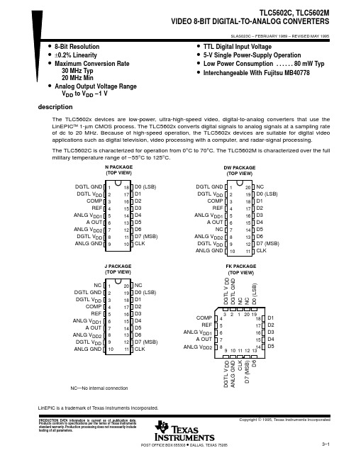
TLC5602中文资料
IMPORTANT NOTICETexas Instruments (TI) reserves the right to make changes to its products or to discontinue any semiconductor product or service without notice, and advises its customers to obtain the latest version of relevant information to verify, before placing orders, that the information being relied on is current.TI warrants performance of its semiconductor products and related software to the specifications applicable at the time of sale in accordance with TI’s standard warranty. Testing and other quality control techniques are utilized to the extent TI deems necessary to support this warranty. Specific testing of all parameters of each device is not necessarily performed, except those mandated by government requirements.Certain applications using semiconductor products may involve potential risks of death, personal injury, or severe property or environmental damage (“Critical Applications”).TI SEMICONDUCTOR PRODUCTS ARE NOT DESIGNED, INTENDED, AUTHORIZED, OR WARRANTED TO BE SUITABLE FOR USE IN LIFE-SUPPORT APPLICATIONS, DEVICES OR SYSTEMS OR OTHER CRITICAL APPLICATIONS.Inclusion of TI products in such applications is understood to be fully at the risk of the customer. Use of TI products in such applications requires the written approval of an appropriate TI officer. Questions concerning potential risk applications should be directed to TI through a local SC sales office.In order to minimize risks associated with the customer’s applications, adequate design and operating safeguards should be provided by the customer to minimize inherent or procedural hazards.TI assumes no liability for applications assistance, customer product design, software performance, or infringement of patents or services described herein. Nor does TI warrant or represent that any license, either express or implied, is granted under any patent right, copyright, mask work right, or other intellectual property right of TI covering or relating to any combination, machine, or process in which such semiconductor products or services might be or are used.Copyright © 1995, Texas Instruments Incorporated。
Brainboxes ED-560UK 产品介绍说明书

Integral DIN mount and slim design takes up minimal cabinet space+5 to +30 Volt Power Input enables the device to be run from USB, a vehicle battery or the factory floorNon conducting polyamide casing with removablenumbered terminal blocks for easy wiring GB AEOF 00031/11Ethernet to Analogue I/O• 4 Analogue Outputs - Selectable as either current or Voltage • Supports simple ASCII or industry standard Modbus TCP • 1 Ethernet Port• -30°C to +80°C/-22ºF to +176ºF Temperature range • Software APIs for VB, C# and more4 Analogue OutputsED-560ConnectorsScrew Terminals 3.5mm pitch, #22 - #14, 0.5mm 2-2.5mm 2 pin power supplyWire Thickness0.150 inch, 3.81mm, 20 pins, 12+8 screw terminals, #26 - #16 AWG, 0.14mm 2-1.3mm 2Power SupplyPower Supply input Unregulated +5V to +30Volts DC, reverse polarity protection Isolation1500V RMS Magnetic isolation from Ethernet EnvironmentalOperating Temperature -30o C to +80o C / -22ºF to +176ºF Storage Temperature-40o C to +85o C / -40ºF to +185ºF Ambient Relative Humidity 5 to 95% (non-condensing)Magjack LED Information Link/Activity LED Solid greenConnection established Flashing Green Data communication Speed LED Green 100Base-Tx Unlit10Base-TEthernetEthernet Port RJ45 jack, 10/100Mhz autosensing, crossover auto sensing (Auto MDIX)Protection 1,500 Volts magnetic isolation between ports HousingIP-20 rated non-conducting polyamide caseEasy Wire Removable screw terminal blocksWide Range Input Power: +5VDC to +30VDCIntegral DIN rail clip with earthIP20 Non-conductingpolyamide case with vents-30ºC to +80ºC/-22ºF to +176ºF temperature rangeEthernet PortSerial Expansion Port suitable for ADAM modulesView from webpage - no software requiredIntegrate with popularsoftware packages or use with our free APIsSupports Modbus TCP or ASCII commands4 Analogue Output LinesEthernet to Analogue OutputED-560Ethernet Port Pin Outs PIN FUNCTION 1RD+ / TD+2RD- / TD-3TD+ / RD+4NC 5NC 6TD- / RD-7NC 8NCLifetime Warranty and Support:We can help with every aspect of your project, from getting you up and running to custom application.Terminal Block Pin OutsTerminal Block Pin 1Pin 2Pin 3Pin 4Pin 5Yellow AGND Vout 0Vout 1Iout 0Iout 1Grey SIG GND RS-485 D-RS-485 D+RS-485 D+RS-485 D-Green AGND Vout 2Vout 3Iout 2Iout 3Black-V+VA+VB-VFunc GNDPower Input +5V to +30V DCEthernet to Analogue OutputED-560Analogue Channels - 4 Outputs IO Protocols DCON ASCII over TCP or COM Port; Modbus TCP Description 4 Analogue OutputsOutput Isolation Yes, Outputs Isolated from Power, Network and Gateway Port Voltage Output Range 0-10VCurrent Output Ranges 0-20mA or 4-20mACurrent Output Type Sink (requires external current source)Output Resolution 12 BitWatchdogSets outputs to predefined values on timeout Max Output Load Current (voltage mode)±5mA Max Output Load Voltage (current mode)30V Dropout Voltage (Current Mode)2.8VOutput Accuracy0.1% of FSR @ 25 °C (77 °F)Output Drift (Voltage Mode) Zero drift less than 30µV/°C, span drift less than 25ppm/°C Output Drift (Current Mode) Zero drift less than 0.2µA/°C, span drift less than 25ppm/°C Output Slew Rate Voltage Mode: 170 kV/s, Current Mode: 4.3A/s Output Settling TimeVoltage Mode: 350µs, Current Mode: 4 µsSerial Expansion Port - RS485Half Duplex RS485 port allows connection and control of industry standard NuDAM, eDAM and ADAM modules using ASCII protocols.Power Supply Power Supply input Unregulated +5V to +30Volts DC, reverse polarity protection Isolation1500V RMS Magnetic isolation from Ethernet Ethernet to Analogue OutputED-560Full command tables can be found in the device manualSoftwareOS Compatibility Brainboxes’ software provides a TCP or Serial COM port interface . Allsoftware versions and updates available to download from our website.Microsoft Legacy COM port drivers for Microsoft OS up to latest Windows 10OtherTCP and web browser interface for other OSs & Linux, e.g. Android, Raspberry PiBoost.IO ManagerLets you find, install and upgrade devicesIndustry Standard PackagesThe COM port based driver means devices are compatible with popular packages such as: LabView, MATLAB, Agilent VEE. So you can continue to get value from your existing development and process control system.Software PlatformsAPIs and sample program code for: Microsoft .NET, C#, Visual Basic, C++,JavaScript, PHP, Java, Objective-C, Python and more - ModbusDevice works as a Modbus TCP server. Modbus TCP can be used on the input and output lines.Modbus access typeSupported Modbus function codes Logical address 984 style address IEC 61131address Read DI counter values Holding register 30x0000...40001...%MW0…Clear DI counters Coil 5, 150x0200...00513%M512…Set/read digital outputsCoil1, 5, 150x0000...00001...%M0…ASCIIThe ED device’s webpage has an interactive ASCII console where any command can be entered and it is immediately executed showing the device’s response.$01M read the name of device address 01 !01ED-588device 01 replies that its name is ED-588$01F read firmware version number of device address 01 !012.54firmware version of device 01 is 2.54//********************ED RangeRemote I/O products available in a range of formats and specifications.PW-650Power supply with USBconnector and prewired screw terminal block. Suitable for use with 5V USB ports.PW-600Power supply with connectors for UK, USA, EU and AUS mains socket. ‘Tails’ are suitable for connecting to screw terminal blocks.Packaging Information PackagingInstallation CD including manual, Microsoft signed drivers & utilities, Quick Start Guide DevicePackaged Weight 0.197 kg, 6.95 ouncesPackaged Dims 160x135x49 mm, 6.3x5.3x1.9 inches GTIN Universal Code 837324003505ApprovalsIndustry Approvals Microsoft Certified Gold Partner, WEEE, RoHS, AEO (C-TPAT), CE Product Support Warranty Lifetime - online registration requiredSupportLifetime Web, Email and Phone Support from fully qualified, friendly staff who work in and alongside the Product Development Team Additional Information OEM option Available for bulk buy OEMMade In Manufactured in the UK by Brainboxes Winner 2005 European Electronics Industry Awards ‘Manufacturer of the Year’CustomisableBrainboxes operate a ‘Perfect Fit Custom Design’ policy for volume users. Moreinfo:********************© Brainboxes 2016BBEDI161002Ethernet to Analogue OutputED-560。
- 1、下载文档前请自行甄别文档内容的完整性,平台不提供额外的编辑、内容补充、找答案等附加服务。
- 2、"仅部分预览"的文档,不可在线预览部分如存在完整性等问题,可反馈申请退款(可完整预览的文档不适用该条件!)。
- 3、如文档侵犯您的权益,请联系客服反馈,我们会尽快为您处理(人工客服工作时间:9:00-18:30)。
50 MHz to 4.0 GHzRF/IF Gain BlockADL5602 Rev. 0Information furnished by Analog Devices is believed to be accurate and reliable. However, noresponsibility is assumed by Analog Devices for its use, nor for any infringements of patents or other rights of third parties that may result from its use. Specifications subject to change without notice. No license is granted by implication or otherwise under any patent or patent rights of Analog Devices. T rademarks and registered trademarks are the property of their respective owners. O ne Technology Way, P.O. Box 9106, Norwood, MA 02062-9106, U.S.A. Tel: 781.329.4700 Fax: 781.461.3113 ©2009 Analog Devices, Inc. All rights reserved.FEATURESFixed gain of 20 dBOperation from 50 MHz to 4.0 GHz Highest dynamic range gain block Input/output internally matched to 50 Ω Integrated bias control circuitOIP3 of 42.0 dBm at 2.0 GHzP1dB of 19.3 dBm at 2.0 GHzNoise figure of 3.3 dB at 2.0 GHzSingle 5 V power supplyLow quiescent current of 89 mA Thermally efficient SOT-89 package ESD rating of ±1.5 kV (Class 1C) FUNCTIONAL BLOCK DIAGRAM RFIN GND RFOUT819-1Figure 1.GENERAL DESCRIPTIONThe ADL5602 is a broadband 20 dB linear amplifier that operates at frequencies up to 4 GHz. The device can be used in a wide variety of cellular, CATV, military, and instrumentation equipment. The ADL5602 provides the highest dynamic range available from an internally matched gain block. This is accomplished by providing extremely low noise figures and very high OIP3 specifications simultaneously, across the entire 4 GHz frequency range.The ADL5602 provides a gain of 20 dB, which is stable over frequency, temperature, power supply, and from device to device. The device is internally matched to 50 Ω at the input and output, making the ADL5602 very easy to implement in a wide variety of applications. Only input/output ac coupling capacitors, power supply decoupling capacitors, and an external inductor are required for operation. The ADL5602 is fabricated on an InGaP HBT process and has an ESD rating of ±1.5 kV (Class 1C). The device is available in a thermally efficient SOT-89 package.The ADL5602 consumes 89 mA on a single 5 V supply and is fully specified for operation from −40°C to +85°C.A fully populated RoHS-compliant evaluation board is available.ADL5602Rev. 0 | Page 2 of 16TABLE OF CONTENTSFeatures .............................................................................................. 1 Functional Block Diagram .............................................................. 1 General Description ......................................................................... 1 Revision History ............................................................................... 2 Specifications ..................................................................................... 3 Typical Scattering Parameters (S Parameters) .......................... 5 Absolute Maximum Ratings ............................................................ 7 ESD Caution .................................................................................. 7 Pin Configuration and Function Descriptions ............................. 8 Typical Performance Characteristics ............................................. 9 Basic Connections .......................................................................... 11 Soldering Information and RecommendedPCB Land Pattern ....................................................................... 11 W-CDMA ACPR Performance .................................................... 12 Evaluation Board ............................................................................ 13 Outline Dimensions ....................................................................... 14 Ordering Guide .. (14)REVISION HISTORY6/09—Revision 0: Initial VersionADL5602Rev. 0 | Page 3 of 16SPECIFICATIONSV CC = 5 V and T A = 25°C, unless otherwise noted. Table 1.Parameter Conditions Min Typ Max UnitOVERALL FUNCTION Frequency Range 50 4000 MHz FREQUENCY = 50 MHzGain 18.3 dB Output 1 dB Compression Point (P1dB) 18.0 dBm Output Third-Order Intercept (OIP3) Δf = 1 MHz, output power (P OUT ) = 0 dBm per tone 27.5 dBm Second Harmonic P OUT = 0 dBm −40.5 dBc Third Harmonic P OUT = 0 dBm −46.1 dBc Noise Figure 2.9 dB FREQUENCY = 140 MHz Gain 17.0 dB vs. Frequency ±50 MHz ±1.2 dB vs. Temperature −40°C ≤ T A ≤ +85°C ±0.03 dB vs. Supply Voltage 4.75 V to 5.25 V ±0.04 dB Output 1 dB Compression Point (P1dB) 18.3 dBm Output Third-Order Intercept (OIP3) Δf = 1 MHz, output power (P OUT ) = 0 dBm per tone 25.0 dBm Second Harmonic P OUT = 0 dBm −45.1 dBc Third Harmonic P OUT = 0 dBm −55.1 dBc Noise Figure 2.9 dB FREQUENCY = 350 MHz Gain 19.7 dB vs. Frequency ±50 MHz ±0.20 dB vs. Temperature −40°C ≤ T A ≤ +85°C ±0.31 dB vs. Supply Voltage 4.75 V to 5.25 V ±0.01 dB Output 1 dB Compression Point (P1dB) 20.0 dBm Output Third-Order Intercept (OIP3) Δf = 1 MHz, output power (P OUT ) = 0 dBm per tone 36.5 dBm Second Harmonic P OUT = 0 dBm −49.9 dBc Third Harmonic P OUT = 0 dBm −83.7 dBc Noise Figure 3.0 dB FREQUENCY = 700 MHz Gain 19.0 20.2 21.0 dB vs. Frequency ±50 MHz ±0.01 dB vs. Temperature −40°C ≤ T A ≤ +85°C ±0.28 dB vs. Supply Voltage 4.75 V to 5.25 V ±0.01 dB Output 1 dB Compression Point (P1dB) 19.0 20.1 dBm Output Third-Order Intercept (OIP3) Δf = 1 MHz, output power (P OUT ) = 0 dBm per tone 38.5 dBm Second Harmonic P OUT = 0 dBm −50.3 dBc Third Harmonic P OUT = 0 dBm −78.4 dBc Noise Figure3.0 dBADL5602Parameter Conditions Min Typ Max Unit FREQUENCY = 900 MHzGain 19.0 20.2 21.0 dB vs. Frequency ±50 MHz ±0.01 dB vs. Temperature −40°C ≤ T A ≤ +85°C ±0.28 dB vs. Supply Voltage 4.75 V to 5.25 V ±0.01 dB Output 1 dB Compression Point (P1dB) 19.0 20.1 dBm Output Third-Order Intercept (OIP3) Δf = 1 MHz, output power (P OUT) = 0 dBm per tone 40.0 dBm Second Harmonic P OUT = 0 dBm −59.4 dBc Third Harmonic P OUT = 0 dBm −77.3 dBc Noise Figure 2.9 dB FREQUENCY = 2000 MHzGain 19.5 dB vs. Frequency ±50 MHz ±0.04 dB vs. Temperature −40°C ≤ T A ≤ +85°C ±0.35 dB vs. Supply Voltage 4.75 V to 5.25 V ±0.04 dB Output 1 dB Compression Point (P1dB) 19.3 dBm Output Third-Order Intercept (OIP3) Δf = 1 MHz, output power (P OUT) = 0 dBm per tone 42.0 dBm Second Harmonic P OUT = 0 dBm −53.1 dBc Third Harmonic P OUT = 0 dBm −60.7 dBc Noise Figure 3.3 dB FREQUENCY = 2600 MHzGain 19.2 dB vs. Frequency ±50 MHz ±0.01 dB vs. Temperature −40°C ≤ T A ≤ +85°C ±0.28 dB vs. Supply Voltage 4.75 V to 5.25 V ±0.05 dB Output 1 dB Compression Point (P1dB) 18.7 dBm Output Third-Order Intercept (OIP3) Δf = 1 MHz, output power (P OUT) = 0 dBm per tone 36.5 dBm Second Harmonic P OUT = 0 dBm −52.8 dBc Third Harmonic P OUT = 0 dBm −67.4 dBc Noise Figure 3.4 dB FREQUENCY = 3500 MHzGain 19.3 dB vs. Frequency ±50 MHz ±0.03 dB vs. Temperature −40°C ≤ T A ≤ +85°C ±0.37 dB vs. Supply Voltage 4.75 V to 5.25 V ±0.07 dB Output 1 dB Compression Point (P1dB) 17.4 dBm Output Third-Order Intercept (OIP3) Δf = 1 MHz, output power (P OUT) = 0 dBm per tone 31.5 dBm Second Harmonic P OUT = 0 dBm −42.9 dBc Third Harmonic P OUT = 0 dBm −66.4 dBc Noise Figure 3.8 dB FREQUENCY = 4000 MHzGain 18.5 dB vs. Frequency ±50 MHz ±0.19 dB vs. Temperature −40°C ≤ T A ≤ +85°C ±0.73 dB vs. Supply Voltage 4.75 V to 5.25 V ±0.08 dB Output 1 dB Compression Point (P1dB) 15.2 dBm Output Third-Order Intercept (OIP3) Δf = 1 MHz, output power (P OUT) = 0 dBm per tone 28.0 dBm Second Harmonic P OUT = 0 dBm −44.1 dBc Third Harmonic P OUT = 0 dBm −64.0 dBc Noise Figure 4.2 dBRev. 0 | Page 4 of 16ADL5602Rev. 0 | Page 5 of 16Parameter Conditions Min Typ Max UnitPOWER INTERFACE VCCSupply Voltage (V CC ) 4.5 5 5.5 V Supply Current 89 106 mA vs. Temperature −40°C ≤ T A ≤ +85°C ±3 mA Power Dissipation V CC = 5 V 0.45 WTYPICAL SCATTERING PARAMETERS (S PARAMETERS)V CC = 5 V and T A = 25°C, the effects of the test fixture have been de-embedded up to the pins of the device. Table 2.Frequency(MHz)S11 S21 S12 S22 Magnitude (dB) Angle (°) Magnitude (dB) Angle (°) Magnitude (dB) Angle (°) Magnitude (dB) Angle (°) 50 −12.75 +32.81 18.14 +163.00 −25.27 −9.54 −8.96 −145.86 100 −8.98 −7.00 15.77 −179.92 −27.59 +4.56 −7.07 −178.96 150 −10.11 −34.04 17.27 −169.01 −26.11 +16.05 −7.89 +159.89 200 −11.97 −50.46 18.50 −168.73 −24.84 +16.55 −9.33 +147.22 250 −13.85 −62.42 19.21 −171.01 −24.14 +14.79 −10.87 +140.02 300 −15.69 −72.90 19.64 −173.77 −23.70 +12.89 −12.23 +136.16 350 −17.40 −81.30 19.90 −176.45 −23.43 +11.02 −13.56 +134.03 400 −19.17 −88.48 20.07 −178.86 −23.26 +9.65 −14.79 +132.79 450 −20.86 −97.45 20.18 +178.79 −23.14 +8.07 −15.99 +132.72 500 −22.52 −107.32 20.25 +176.86 −23.08 +7.11 −17.02 +133.33 550 −24.32 −112.89 20.32 +174.84 −23.00 +6.15 −18.21 +133.04 600 −26.07 −120.03 20.35 +173.09 −22.97 +5.24 −19.45 +135.06 650 −27.89 −128.79 20.39 +171.35 −22.93 +4.35 −20.73 +136.29 700 −30.79 −133.19 20.42 +169.67 −22.91 +3.72 −22.22 +136.96 750 −34.53 −136.03 20.42 +167.93 −22.91 +2.93 −23.91 +135.39 800 −42.59 −130.76 20.46 +166.48 −22.88 +2.30 −26.35 +136.07 850 −46.49 −2.93 20.47 +164.85 −22.88 +1.67 −29.40 +132.08 900 −34.26 +15.99 20.47 +163.17 −22.86 +0.98 −34.27 +116.48 950 −29.55 +9.83 20.48 +161.77 −22.86 +0.39 −40.86 +41.72 1000 −25.87 +5.52 20.48 +160.25 −22.86 −0.21 −31.44 −10.36 1050 −23.03 +1.85 20.47 +158.65 −22.89 −0.84 −26.19 −18.99 1100 −21.25 +0.10 20.45 +157.18 −22.90 −1.43 −23.27 −22.34 1150 −19.31 −1.89 20.45 +155.50 −22.92 −2.06 −20.70 −22.26 1200 −17.72 −4.09 20.40 +153.93 −22.96 −2.72 −18.67 −24.44 1250 −16.13 −6.53 20.35 +152.44 −23.04 −3.38 −16.92 −24.75 1300 −14.81 −8.71 20.31 +150.88 −23.07 −4.04 −15.44 −25.79 1350 −13.65 −10.01 20.24 +149.35 −23.16 −4.60 −14.14 −25.36 1400 −12.68 −11.33 20.18 +147.91 −23.22 −5.06 −13.12 −25.73 1450 −11.72 −12.65 20.11 +146.40 −23.32 −5.76 −12.04 −25.59 1500 −10.92 −13.56 20.04 +145.13 −23.39 −6.16 −11.20 −25.40 1550 −10.21 −14.37 19.97 +143.86 −23.49 −6.54 −10.49 −25.60 1600 −9.58 −15.37 19.88 +142.58 −23.57 −6.93 −9.77 −25.59 1650 −9.05 −15.74 19.80 +141.40 −23.69 −7.16 −9.21 −25.31 1700 −8.52 −16.73 19.72 +140.23 −23.76 −7.45 −8.66 −25.42 1750 −8.13 −17.13 19.64 +139.13 −23.87 −7.60 −8.26 −25.32 1800 −7.76 −17.59 19.57 +138.12 −23.94 −7.80 −7.91 −24.96 1850 −7.46 −17.76 19.50 +137.16 −24.05 −7.88 −7.56 −24.77 1900 −7.19 −17.92 19.43 +136.25 −24.13 −7.91 −7.35 −24.46 1950 −6.98 −17.84 19.39 +135.31 −24.18 −7.94 −7.13 −23.92ADL5602Rev. 0 | Page 6 of 16Frequency(MHz)S11 S21 S12 S22 Magnitude (dB) Angle (°) Magnitude (dB) Angle (°) Magnitude (dB) Angle (°) Magnitude (dB) Angle (°) 2000 −6.85 −18.00 19.35 +134.44 −24.26 −7.99 −6.96 −23.55 2050 −6.74 −17.93 19.31 +133.61 −24.29 −7.91 −6.86 −22.70 2100 −6.63 −17.57 19.29 +132.74 −24.37 −7.81 −6.75 −22.45 2150 −6.66 −17.34 19.25 +132.06 −24.42 −7.58 −6.76 −22.01 2200 −6.65 −17.26 19.29 +131.19 −24.40 −7.63 −6.78 −21.42 2250 −6.69 −17.10 19.30 +130.47 −24.41 −7.59 −6.82 −20.82 2300 −6.77 −16.90 19.33 +129.54 −24.42 −7.40 −6.87 −20.25 2350 −6.87 −16.65 19.36 +128.72 −24.40 −7.46 −7.04 −19.57 2400 −7.05 −16.25 19.42 +127.81 −24.38 −7.50 −7.20 −18.85 2450 −7.22 −16.11 19.49 +126.89 −24.35 −7.46 −7.42 −18.17 2500 −7.45 −16.00 19.53 +125.82 −24.31 −7.75 −7.66 −17.76 2550 −7.64 −15.84 19.58 +124.74 −24.31 −7.86 −7.91 −17.18 2600 −7.95 −15.66 19.66 +123.61 −24.25 −8.20 −8.29 −16.64 2650 −8.29 −15.64 19.74 +122.46 −24.19 −8.54 −8.66 −16.15 2700 −8.62 −15.95 19.81 +121.20 −24.17 −8.90 −8.97 −15.97 2750 −8.95 −15.92 19.89 +119.91 −24.13 −9.35 −9.41 −15.67 2800 −9.31 −16.23 19.94 +118.47 −24.08 −9.95 −9.87 −15.96 2850 −9.67 −16.74 20.03 +117.02 −24.05 −10.55 −10.34 −16.17 2900 −9.99 −17.33 20.07 +115.47 −24.07 −11.17 −10.83 −16.68 2950 −10.28 −18.00 20.14 +113.95 −24.02 −11.71 −11.28 −17.66 3000 −10.53 −19.16 20.18 +112.28 −24.03 −12.51 −11.69 −19.15 3050 −10.69 −20.29 20.21 +110.53 −24.10 −13.72 −12.17 −21.42 3100 −10.86 −21.94 20.25 +108.77 −24.04 −14.66 −12.54 −24.24 3150 −10.91 −23.61 20.27 +107.15 −24.09 −15.23 −12.83 −27.07 3200 −10.70 −25.42 20.28 +105.16 −24.18 −16.23 −12.92 −32.00 3250 −10.57 −27.33 20.28 +103.09 −24.17 −17.39 −13.04 −36.71 3300 −10.38 −29.60 20.26 +101.20 −24.22 −18.24 −12.99 −42.66 3350 −9.92 −31.76 20.21 +99.05 −24.39 −20.06 −12.57 −48.16 3400 −9.48 −34.25 20.15 +96.98 −24.49 −20.74 −12.19 −54.36 3450 −8.98 −36.47 20.08 +94.93 −24.61 −21.69 −11.64 −59.44 3500 −8.44 −38.18 20.00 +92.80 −24.72 −23.44 −11.00 −64.07 3550 −7.92 −40.32 19.90 +90.88 −24.88 −24.35 −10.34 −68.43 3600 −7.34 −42.20 19.74 +88.69 −25.15 −25.31 −9.59 −72.77 3650 −6.79 −43.72 19.57 +86.66 −25.35 −26.95 −8.90 −76.09 3700 −6.29 −45.15 19.41 +84.80 −25.56 −27.76 −8.29 −79.17 3750 −5.82 −46.51 19.23 +82.83 −25.90 −28.90 −7.69 −81.76 3800 −5.37 −47.51 19.00 +81.05 −26.16 −29.05 −7.12 −84.30 3850 −4.93 −48.36 18.78 +79.53 −26.46 −30.35 −6.65 −86.42 3900 −4.56 −48.94 18.55 +78.02 −26.81 −29.93 −6.20 −88.14 3950 −4.23 −49.33 18.32 +76.71 −27.08 −31.04 −5.83 −89.69 4000 −3.97 −49.71 18.08 +75.39 −27.50 −30.65 −5.50 −91.14ADL5602Rev. 0 | Page 7 of 16ABSOLUTE MAXIMUM RATINGSESD CAUTIONTable 3.Parameter Rating Supply Voltage, V CC 6.5 V Input Power (re: 50 Ω) 16 dBm Internal Power Dissipation (Paddle Soldered) 600 mW θJA (Junction to Air) 30.7°C/W θJC (Junction to Paddle) 5.0°C/W Maximum Junction Temperature 150°C Lead Temperature (Soldering, 60 sec) 240°C Operating Temperature Range −40°C to +85°C Storage Temperature Range −65°C to +150°CStresses above those listed under Absolute Maximum Ratings may cause permanent damage to the device. This is a stress rating only; functional operation of the device at these or any other conditions above those indicated in the operationalsection of this specification is not implied. Exposure to absolute maximum rating conditions for extended periods may affect device reliability.ADL5602Rev. 0 | Page 8 of 16PIN CONFIGURATION AND FUNCTION DESCRIPTIONSRFINGNDRFOUT 123GNDADL5602TOP VIEW (Not to Scale)(2)08190-002Figure 2. Pin ConfigurationTable 4. Pin Function DescriptionsPin No. Mnemonic Description1 RFIN RF Input. This pin requires a dc blocking capacitor.2 GNDGround. Connect this pin to a low impedance ground plane.3 RFOUT RF Output and Supply Voltage. DC bias is provided to this pin through an inductor that is connected to the external power supply. The RF path requires a dc blocking capacitor.(2)Exposed PaddleExposed Paddle. Internally connected to GND. Solder to a low impedance ground plane.ADL5602Rev. 0 | Page 9 of 16TYPICAL PERFORMANCE CHARACTERISTICS5101520253035404500.40.8 1.2 1.6 2.0 2.4 2.8 3.2 3.6 4.0N F , G A I N , P 1d B , O I P 3 (d B , dB m )FREQUENCY (GHz)08190-003Figure 3. Noise Figure, Gain, P1dB, and OIP3 vs. Frequency16.517.017.518.018.519.019.520.020.521.000.40.8 1.2 1.6 2.0 2.4 2.8 3.2 3.6 4.0G A I N(d B )FREQUENCY (GHz)08190-004Figure 4. Gain vs. Frequency and Temperature–50–45–40–35–30–25–20–15–10–5000.40.8 1.2 1.6 2.0 2.4 2.8 3.2 3.6 4.0S -P A R A M E T E R S (d B )FREQUENCY (GHz)08190-005Figure 5. Input Return Loss (S11), Output Return Loss (S22), andReverse Isolation (S12) vs. Frequency 0510152025303540451214161820222426283000.51.01.52.02.53.03.54.0O I P 3 (d B m )P 1d B (d B m )FREQUENCY (GHz)08190-006Figure 6. P1dB and OIP3 vs. Frequency and Temperature20222426283032343638404244–5–3–11357911131517O I P 3 (d B m )P OUT PER TONE (dBm)08190-007Figure 7. OIP3 vs. Output Power (P OUT ) and Frequency2.02.42.83.23.64.04.44.85.25.6N O I S E F I G U R E (d B )FREQUENCY (GHz)08190-008Figure 8. Noise Figure vs. Frequency and TemperatureADL5602Rev. 0 | Page 10 of 16H2H3H A R M O N I C S (d B c )–90–80–70–60–50–40–30FREQUENCY (GHz)0.50 1.0 1.5 2.0 2.5 3.03.54.008190-009Figure 9. Single Tone Harmonics vs. Frequency , P OUT = 0 dBm5101520253018.819.019.219.419.619.820.0P E R C E N T A G E (%)GAIN (dB)08190-010Figure 10. Gain Distribution at 2000 MHz051015202530P E R C E N T A G E (%)P1dB (dBm)08190-011Figure 11. P1dB Distribution at 2000 MHz5101520253035404532343638404244464850P E R C E N T A G E (%)OIP3 (dBm)08190-020Figure 12. OIP3 Distribution at 2000 MHz, P OUT = 0 dBm1020304050607080 2.6 2.8 3.0 3.2 3.4 3.6 3.8 4.0P E R C E N T A G E (%)NOISE FIGURE (dB)08190-021Figure 13. Noise Figure Distribution at 2000 MHz80828486889092949698–40–30–20–100102030405060708090S U P P L Y C U R R E N T (m A )TEMPERATURE (°C)08190-014Figure 14. Supply Current vs. TemperatureADL5602Rev. 0 | Page 11 of 16BASIC CONNECTIONS The basic connections for operating the ADL5602 are shown in Figure 15. Recommended components are listed in Table 5. The input and output should be ac-coupled with appropriately sized capacitors (device characterization was performed with 0.1 μF capacitors). A 5 V dc bias is supplied to the amplifier through the bias inductor connected to RFOUT (Pin 3). The bias voltage should be decoupled using a 1 μF capacitor, a 1.2 nF capacitor, and a 68 pF capacitor.08190-015 Figure 15. Basic ConnectionsSOLDERING INFORMATION AND RECOMMENDEDPCB LAND PATTERNFigure 16 shows the recommended land pattern for the ADL5602.To minimize thermal impedance, the exposed paddle on thepackage underside should be soldered down to a ground planealong with Pin 2. If multiple ground layers exist, they should bestitched together using vias. For more information on landpattern design and layout, refer to AN-772 Application Note, ADesign and Manufacturing Guide for the Lead Frame Chip ScalePackage (LFCSP).08190-016Figure 16. Recommended Land PatternTable 5. Recommended Components for Basic ConnectionsFrequency (MHz) C1 C2 L1C4 C5 C6 50 to 4000 0.1 μF 0.1 μF 470 nH (Coilcraft 0603LS-NX or equivalent) 68 pF 1.2 nF 1 μFADL5602Rev. 0 | Page 12 of 16W-CDMA ACPR PERFORMANCEFigure 17 shows a plot of adjacent channel power ratio (ACPR) vs. P OUT for the ADL5602. The signal type being used is a single W-CDMA carrier (Test Model 1-64) at 2140 MHz. This signal is generated by a very low ACPR source. ACPR is measured at the output by a high dynamic range spectrum analyzer, which incorporates an instrument noise correction function. The ADL5602 achieves an ACPR of −75 dBc at −5 dBm output, at which point device noise and not distortion is beginning to dominate the power in the adjacent channels. At an output power of +5 dBm, ACPR is still very low at −61 dBc, makingthe device particularly suitable for PA driver applications.–40–45–50–55–60–65–70–75–80–20–15–10–50510A C P R A T 5M H z C A R R I E R O F F S ET (d B c )P OUT (dBm)08190-017Figure 17. ACPR vs. P OUT , Single Carrier W-CDMA (Test Model 1-64) at2140 MHz Evaluation BoardADL5602Rev. 0 | Page 13 of 16EVALUATION BOARD Figure 19 shows the schematic for the ADL5602 evaluation board. The board is powered by a single 5 V supply. The components used on the board are listed in Table 6. Power can be applied to the board through clip-on leads(VCC and GND). 08190-018Figure 18. Evaluation Board Layout (Top)08190-019Figure 19. Evaluation Board SchematicTable 6. Evaluation Board Configuration OptionsComponent DescriptionDefault Value C1, C2 AC-coupling capacitors0.1 μF, 0402 L1 DC bias inductor470 nH, 0603 (Coilcraft 0603LS-NX or equivalent) VCC and GND Clip-on terminals for power supplyC4, C5, C6 Power supply decoupling capacitors C4 = 68 pF, 0603; C5 = 1.2 nF, 0603; C6 = 1 μF, 1206ADL5602Rev. 0 | Page 14 of 16OUTLINE DIMENSIONS121808-B *COMPLIANT TO JEDEC STANDARDS TO-243 WITHEXCEPTION TO DIMENSIONS INDICATED BY AN ASTERISK.2.29 Figure 20. 3-Lead Small Outline Transistor Package [SOT-89](RK-3)Dimensions shown in millimetersORDERING GUIDEModel Temperature Range Package Description Package Option ADL5602ARKZ-R71 −40°C to +85°C3-Lead SOT-89, 7“ Tape and Reel RK-3 ADL5602-EVALZ 1Evaluation Board1 Z = RoHS Compliant Part.ADL5602 NOTESRev. 0 | Page 15 of 16ADL5602Rev. 0 | Page 16 of 16 NOTES©2009 Analog Devices, Inc. All rights reserved. Trademarks and registered trademarks are the property of their respective owners.D08190-0-6/09(0)。