CAT811LEUS-T中文资料
Cambridge CMOS Sensors CCS811 NTC Thermistor接口指南说明

Cambridge CMOS Sensorsis nowMember of theams GroupContact information:Headquarters:ams AGTobelbader Strasse 308141 Premstaetten, AustriaTel: +43 (0) 3136 500 0e-Mail: *****************Key Benefits∙Simple circuity fordetermining temperature ∙Cost effective andminimal PCB footprint∙Integrated MCU with ADC ∙I2C digital interface∙Optimised low-powermodes∙Compact 2.7x4.0 mm LGA package∙Proven technologyplatform∙On-board processing to reduce requirement onhost processor∙Fast time-to-market∙Extended battery life∙Reduced componentcount∙Suitable for small form factor designs∙Highly reliable solution Applications∙IAQ monitoring forSmarthome, Smartphonesand accessoriesVoltage Divider and ADCTo enable the NTC circuit a voltage divider circuit is constructed between the VDD, AUX and Sense pins. Refer to Figure 1 below.Figure 1 CCS811 NTC Voltage Divider CircuitThe CCS811 has an internal ADC that can measure the voltages at VDD, AUX and Sense, enabling the CCS811 to calculate the voltages across the Reference Resistor (R REF) and the NTC Resistor (R NTC).For optimal usage of ADC resolution, the value of RREF and the nominal value of RNTC should be approximately the same; the suggested value is 100kΩ.As temperature increases, RNTC decreases. This causes the voltage value sampled on the AUX signal to decrease. The opposite is true when temperature decreases, RNTC increases.Hardware Connection When NTC Is Not RequiredIf the system where the CCS811 is deployed uses another means of obtaining temperature, such as combined temperature and humidity sensor, or if temperature is not measured in the system, then there is no requirement to connect the AUX and Sense pins to the thermistor. There is also no requirement to connect the reference resistor between AUX and VDD. Pins 4 and 5 must still be connected together for normal operation.Determining Thermistor ResistanceThe CCS811 retrieves samples on the Sense and AUX ADCs concurrently, thus obtaining the two voltages, V REF and V NTC. This allows the user to determine the resistance of the NTC thermistor. The following proof using Ohm’s Law can be therefore be used to find the resistance, R NTC , of the NTC thermistor.Iref =VrefRrefIntc =VntcRntcAs Iref = IntcVref Rref =VntcRntcTℎerfore Rntc = Vntc ∗RrefVrefEquation 1 R NTC ProofThe CCS811 NTC mailbox (ID = 6) provides the application with the V REF and V NTC values sampled by the AUX and Sense pins respectively. The format of this data is shown in Table 2 NTC Mailbox Data Encoding.Table 2 NTC Mailbox Data EncodingBoth V REF and V NTC are in millivolts. As R REF is a discrete component with a known magnitude of resistance, and as the CCS811 has provided the V REF and V NTC values it is therefore very simple to determine the R NTC value. In the simplest case when V REF and V NTC are equal, R NTC is equal to R REF .EquationsUsing the Simplified Steinhart Equation to Determine TemperatureAfter determining the value of R REF the thermistor’s data sheet must be consulted in order to understand how this can be used to calculate the ambient temperature. The most common method for this is to use a simplified version of the Steinhart equation. In that case the data sheet will contain an equation of the form shown in Equation 2 Simplified Steinhart Equation.B=log(RRo) 1T−1ToEquation 2 Simplified Steinhart EquationThe equation contains a number of parameters that are found in the NTC thermistor’s data sheet. It also contains some parameters that the user must provide. These are described below in Table 3 Simplified Steinhart Equation Parameter Descriptions.Table 3 Simplified Steinhart Equation Parameter DescriptionsNote that B, T O and R O are constant values that can be found in the thermistor’s data sheet. Also observe that R is the resistance of the thermistor at the current temperature. This value is available to the application after reading the data in the CCS811 NTC mailbox and using Equation 1. Therefore the only unknown value is the temperature, T. This allows Equation 2 to be solved for T by rearranging as shown in Equation 3 Temperature Calculation.1 T =1To+1Blog(RRo)Equation 3 Temperature CalculationThe temperature can then be calculated in software as described in the subsequent sections.P a g e|4© Cambridge CMOS Sensors Ltd, Deanland House, Cowley Road, Cambridge, CB4 0DL, UKThe first step in calculating temperature is to perform a read to the NTC mailbox, this will look something similar to the following, adapt accordingly to the applications drivers and API:i2c_write(CCS_811_ADDRESS, NTC_REG, i2c_buff, size=0);i2c_read(CCS_811_ADDRESS, i2c_buff, size=4);The first I2C transaction is a setup write to the NTC mailbox (the argument NTC_REG has the value 6) with no data. This is followed by a 4 byte read, that access the NTC mailbox and stores these 4 bytes of data to a byte/character array called i2c_buff. Please see CC-000803 Programming and Interfacing Guide for more details on handling the CCS811 I2C interface and timing requirements.The V REF and V NTC in i2c_buff can then be passed to a function that implements Equation 1.#define RREF 100000rntc = calc_rntc((uint16_t)(i2c_buff[0]<<8 | i2c_buff[1]),(uint16_t)(i2c_buff[2]<<8 | i2c_buff[3]));uint32_t calc_rntc(uint16_t vref, uint16_t vntc){return (vntc * RREF / vref);}The value of RREF is the R O taken from the thermistors data sheet. As i2c_buff is an array of chars in this example it will have to be converted to 2x16 bit scalars in order to be passed to the function. It is recommended to do the shifting as this will work on both a big and little endian host processor.The returned rntc value can then be used to determine the temperature.Application Software Running on a CPU with Floating Point SupportIf the CPU running the application has floating point support and sufficient program memory for the floating point calculations and/or library functions then the c standard math library can be used to help implement Equation 3.An example is shown below:#define RNTC_25C 100000#define BCONSTANT 4250#define RNTC_TEMP 25double calc_temp_from_ntc(uint32_t rntc){double ntc_temp;ntc_temp = log((double)rntc / RNTC_25C); // 1ntc_temp /= BCONSTANT; // 2ntc_temp += 1.0 / (RNTC_TEMP + 273.15); // 3ntc_temp = 1.0 / ntc_temp; // 4ntc_temp -= 273.15; // 5return ntc_temp;}Recall Equation 3:1 T =1To+1Blog(RRo)The application developer can extract from thermistors data sheet the constant values in order to solve for temperature. RNTC_25C, BCONSTANT and RNTC_TEMP correspond to R O, B and T O respectively. These can then be written to a c header file used in the application software.Comments for each of the 5 steps in the software example above are as follows:1.Calculate log(R/R O) using the maths library, use the R NTC value calculated from Equation 12.Divide log(R/R O) by the thermistor’s B constant3.Add 1/T O to the interim result, the equation requires all temperatures are in Kelvin. Adding 273.15 toT O converts the value in the thermistor’s data sheet, normally 25o C (RNTC_TEMP), to Kelvin4.The result of 3 is the reciprocal of the temperature so this step yields the current temperature inKelvin5.Convert from Kelvin to o CApplication Software Running on a CPU With No Floating Point SupportIf the application CPU does not have floating point support or there is insufficient program memory available for the library and/or floating point calculations, then the temperature can be determined using linear interpolation between two point on the thermistor’s temperat ure versus resistance curve. Finding the two points can be done as follows:1.The thermistors data sheet can be consulted to find the resistance at various points on the graph,normally in increments of 5o C2.Pre-calculate the resistances at various temperatures required by the application in increments of x o C,where x is application specific.The application software can store the resistance values in an array or lookup table and use the resistance, R NTC calculated using Equation 1, as an input into the look up table. The look up operation must be programmed to return the two resistance points. Basically the goal is to determine which two resistance values R NTC lies between in the lookup mechanism used by the application. Then linear interpolation can then be used to determine a reasonably accurate temperature value.For example assuming that a 100kΩ therm istor has a resistance of 210k at 10o C and 270k at 5o C. Let’s also assume Equation 1 yielded a value of 222000Ωfor R NTC. The following can be used to approximate the temperature.1.The application must determine how many steps between the two points are required. Forexample assuming 100 steps then subtract the high and low resistance and divide by 100:step_size =(270000 – 210000) / 100 = 600Thus each 0.05o C increment in temperature corresponds to 600Ω decrease in resistance betweenthese 2 points2.Calculate how may steps R NTC is from the higher resistance:rntc_steps =(270000 – 222000) / step_size = 803.To avoid errors using integer types, use a few orders of magnitude greater: i.e. lower temp*1000(5x1000 = 5000). As each step is 50 milli o C (0.05x1000) the temperature is therefore:T = 5000 + rntc_steps∗50 = 9000,i.e.9 degrees Celsius.The temperature determined using the NTC thermistor circuit and the equations in the sections above can be used for temperature compensation on the CCS811.When writing the temperature to the ENV_DATA register it is necessary to also write the humidity. If the humidity is not known then the default value corresponding to 50% relative humidity must be written to ENV_DATA. For example if the temperature is 30o C and no RH data is available then the user must write four bytes as follows:0x64, 0x00, 0x6E, 0x00The first two bytes are the RH data in the format required by the CCS811 ENV_DATA register. The next two bytes are the temperature +25o C in the format required by ENV_DATA. Please consult the data sheet for more information. Additionally a full example of using ENV_DATA is available in application note CC-000803-AN Programming and Interfacing Guide.The contents of this document are subject to change without notice. Customers are advised to consult with Cambridge CMOS Sensors (CCS) Ltd sales representatives before ordering or considering the use of CCS devices where failure or abnormal operation may directly affect human lives or cause physical injury or property damage, or where extremely high levels of reliability are demanded. CCS will not be responsible for damage arising from such use. As any devices operated at high temperature have inherently a certain rate of failure, it is therefore necessary to protect against injury, damage or loss from such failures by incorporating appropriate safety measuresAbbreviationsReferences。
MIL-S8TA 8-Port 10 100 1000 BASE-T 未管理开关用户指南(Rev.

MIL-S8TA8-Port 10/100/1000 BASE-T Unmanaged Switch User GuideRev. A22012-09-17Regulatory Approval- FCC Class A- UL 1950- CSA C22.2 No. 950- EN60950- CE- EN55022 Class A- EN55024Canadian EMI NoticeThis Class A digital apparatus meets all the requirements of the Canadian Interference-Causing Equipment Regulations.Cet appareil numerique de la classe A respecte toutes les exigences du Reglement sur le materiel brouilleur du Canada.European NoticeProducts with the CE Marking comply with both the EMC Directive (89/336/EEC) and the Low Voltage Directive (73/23/EEC) issued by the Commission of the European Community Compliance with these directives imply conformity to the following European Norms:EN55022 (CISPR 22) - Radio Frequency InterferenceEN61000-X - Electromagnetic ImmunityEN60950 (IEC950) - Product SafetyFive-Year Limited WarrantyTransition Networks warrants to the original consumer or purchaser that each of it's products,and all components thereof, will be free from defects in material and/or workmanship for aperiod of five years from the original factory shipment date. Any warranty hereunder isextended to the original consumer or purchaser and is not assignable.Transition Networks makes no express or implied warranties including, but not limited to, anyimplied warranty of merchantability or fitness for a particular purpose, except as expressly setforth in this warranty. In no event shall Transition Networks be liable for incidental orconsequential damages, costs, or expenses arising out of or in connection with theperformance of the product delivered hereunder. Transition Networks will in no case coverdamages arising out of the product being used in a negligent fashion or manner.TrademarksThe MiLAN logo and Transition Networks trademarks are registered trademarks of Transition Networks in the United States and/or other countries.To Contact Transition NetworksFor prompt response when calling for service information, have the following information ready:- Product serial number and revision- Date of purchase- Vendor or place of purchaseYou can reach Transition Networks technical support at:E-mail:**********************Telephone: +1.800.260.1312 x 200Fax: +1.952.941.2322Transition Networks6475 City West ParkwayEden Prairie, MN 55344United States of AmericaTelephone: +1.800.526.9267Fax: : +1.952.941.2322*******************© Copyright 2006 Transition NetworksThis equipment has been tested and found to comply with the limits for a class A device, pursuant to part 15 of the FCC rules. These limits are designed to provide reasonable protection against harmful interference in a commercial installation. This equipment generates uses and can radiate radio frequency energy and, if not installed and used in accordance with instructions, may cause harmful interference on radio communications. Operation of this equipment in a residential area is likely to cause harmful interference, in which case, the user will be requires to correct the interference at the user’s own expense.Content Introduction (1)Features (1)Package Contents (2)Hardware Description (3)Physical Dimensions (3)Front Panel (3)LEDs Indicators (3)Rear Panel (4)Installation (6)Attaching Rubber Feet (6)Mounting on the Wall (6)Power On (7)Technical Specification (8)IntroductionThe 8-port 10/100/1000BASE-T Switch with Auto MDI/MDIX is an unmanaged multi-port Switch that can be used to build high-performance switched networks. This switch is a store-and-forward device that offers low latency for high-speed networking. The Switch is designed for the core of the network backbone computing environment to solve traffic block problems at SME (small, medium enterprise) businesses.The 8-port 10/100/1000BASE-T Switch features a “store-and-forward”switching technology. This allows the switch to auto-learn and store source addresses in an 8K-entry MAC address table.Features⏹Conforms to IEEE 802.3, 802.3u, 802.3ab and 802.3x⏹8 Gigabit copper SOHO switch, compact size with universal internalpower⏹Auto-MDIX on all ports⏹16 Gbps back-plane⏹ N-Way Auto-Negotiation⏹8K MAC address table⏹Back pressure half duplex⏹Flow control full duplex⏹ Store-and-Forward switching architecture⏹ 144Kbytes memory buffer⏹True non-blocking switching⏹Support 8Kbytes Jumbo Frame1Package ContentsUnpack the contents of the switch and verify them against the checklist below.⏹ 8-port Switch⏹Power Cord.⏹User Guide.8-port Switch Power Cord User manualPackage ContentCompare the contents of your switch package with the standard checklist above. If any item is missing or damaged, please contact your local dealerfor service.23Hardware DescriptionPhysical DimensionsThe physical dimensions of the Switch is 165mm x 100mm x 32.5 mm (L x W x H)Front PanelThe front panel of the 8-Port Gigabit switch consists of LED-indicators (100/1000, Link/Activity, Full duplex/Collision) for each Gigabit port and power LED-indicator for unit.RJ-45 Ports (Auto MDI/MDIX): 8 10/100/1000 N-way auto-sensing for 10Base-T, 100Base-TX or 1000Base-T connections. (In general, MDI means connecting to another Hub or Switch while MDIX means connecting to a workstation or PC. Therefore, Auto MDI/MDIX allows you to connect to another Switch or workstation without changing to non-crossover or crossover cabling.)LEDs IndicatorsThe LED Indicators gives real-time information of systematic operation status. The following table provides descriptions of LED status and their meaning.Green PowerOnOff Power is not connectedGreen The port is operating at the speed of 1000Mbps.Orange The port is operating at the speed of 100Mbps.Off No device attached or in 10Mbps modeGreen The port is connecting with the device.Blinking The port is receiving or transmitting data.Off Nodeviceattached.Orange The port is operating in Full-duplex mode.Blinking Packet collision occurred on this port.Off No device attached or in half-duplex mode. Rear PanelThe rear panel of the 8-port Gigabit Switch consists of 8 auto-negotiation 10/100/1000Mbps Ethernet RJ-45 connectors (support Automatic4MDI/MDIX function).RJ-45 Ports (Auto MDI/MDIX): 8 port auto-negotiation 10/100/1000 Mbps Ethernet RJ-45 connectors[Auto MDI/MDIX means that you can connect to another Switch or workstation without changing non-crossover or crossover cabling.]5InstallationThis section shows the installation procedures of the switch.Set the Switch on a sufficiently large flat space with a power outlet nearby.The surface where you put your Switch should be clean, smooth, level, and sturdy. Make sure there is enough clearance around the Switch to allow attachment of cables, power cord and air circulation.Attaching Rubber FeetA. Make sure mounting surface on the bottom of the Switch is grease anddust free.B. Remove adhesive backing from your Rubber Feet.C. Apply the Rubber Feet to each corner on the bottom of the Switch.These footpads can prevent the Switch from shock/vibration. Mounting on the WallThe switch can be mounted on the wall. The switch has two wallmountbrackets included in the package.Power OnConnect the cord of power to the power socket on the rear panel of the Switch. The other side of power cord connects to the power outlet. Check the power indicator on the upper panel to see if power is properly supplied.7Technical SpecificationThe following table provides the technical specification of 8-ports Gigabit Switch.IEEE 802.3 10BASE-T EthernetIEEE 802.3u 100BASE-TX Fast EthernetIEEE 802.3ab Gigabit EthernetIEEE 802.3x Flow Control and Back-pressureCSMA/CDStore-and-Forward switching architecture14,880 pps for 10Mbps148,800 pps for 100Mbps1,488,000 pps for 1000MbpsRJ-45; Auto-MDIX on all ports8K Mac address table144Kbytes memory bufferSupports 8Kbytes jumbo packet size16Gbps810BASE-T: 2-pair UTP/STP Cat. 3, 4, 5 cable EIA/TIA-568 100-ohm (100m)100BASE-TX: 2-pair UTP/STP CAT. 5 cable EIA/TIA-568 100-ohm (100m)Gigabit Copper: 4 pair UTP/STP CAT. 5 cable EIA/TIA 568 100-ohm (100M)Per port: 100/1000, Link/Activity, Full duplex/ CollisionPer unit: PowerAC 110~240V, 50/60Hz7.6 Watt (maximum)0℃ to 45℃ (32℉ to 113℉)-40℃ to 70℃ (-40℉ to 158℉)10% to 90% (Non-condensing)0% to 95% (Non-condensing)165mm x 100mm x 32.5mm (L x W x H) Compliance with FCC Class A, CE Compliance UL, cUL,CE/EN609509。
CS8211AEO

电话:0510-8180 5243
传真:0510-8180 5110
无锡华润华晶微电子有限公司
第6页 共6页
无锡华润华晶微电子有限公司
第2页 共6页
CS8211AEO
○R
VOUT
=
NS NP
⋅ R2 + R3 R2
⋅VFB
− VDiode
当 FB 侦 测 电 压 超 过 V FBM AX ,则 系 统 发 生 过 压 保 护 ,系 统 将 进 入 自 动 重 启 过 程 ,如 果 输 出 过 压 状 态 还 没 有 消 除 , 系 统 将 反 复 不 断 尝 试 性 重 启 ( 打 嗝 模 式 )。
NP NS
× I peak
2.2.3 电流检测和前沿消隐
CS8211AEO 芯片侦测 CS 端到 GND 的采样电阻 RCS 上的电压,每个开关周期,变 压器电感电流从 0A 上升,RCS 电压也从 0V 上升,当 RCS 电阻电压超过 0.6V 后,立刻 关断功率管。这样芯片实现逐周期峰值电流限制,严格控制变压器原边电流大小。
最小
最大
5.05
0.37
0.47
1.27
5.80
6.20
3.85
3.95
1.35
1.45
标注 C1 C2 C3 D1 D2
最小
最大
0.575
0.625
0.575
0.625
0.00
0.20
0.40
0.60
4.85
部件名称
引线框 塑封树脂
芯片 内引线 装片胶
说明
产品中有毒有害物质或元素的名称及含量
有毒有害物质或元素
同 样 ,当 FB 侦 测 电 压 低 于 V FBMIN ,则 系 统 发 生 短 路 保 护 ,系 统 将 进 入 自 动 重 启 过 程 , 如 果 输 出 短 路 状 态 还 没 有 消 除 , 系 统 将 反 复 不 断 尝 试 性 重 启 ( 打 嗝 模 式 )。
MEMORY存储芯片MAX811TEUS+T中文规格书
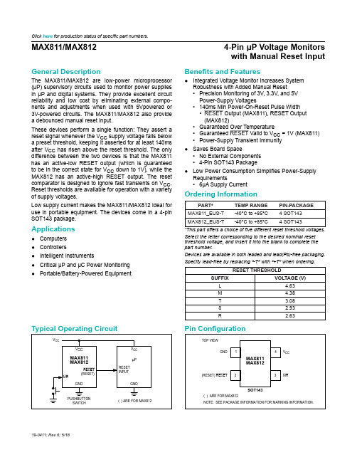
General DescriptionThe MAX811/MAX812 are low-power microprocessor (μP) supervisory circuits used to monitor power supplies in μP and digital systems. They provide excellent circuit reliability and low cost by eliminating external compo-nents and adjustments when used with 5Vpowered or 3V-powered circuits. The MAX811/MAX812 also provide a debounced manual reset input.These devices perform a single function: They assert a reset signal whenever the V CC supply voltage falls below a preset threshold, keeping it asserted for at least 140ms after V CC has risen above the reset threshold. The only difference between the two devices is that the MAX811 has an active-low RESET output (which is guaranteed to be in the correct state for V CC down to 1V), while the MAX812 has an active-high RESET output. The reset comparator is designed to ignore fast transients on V CC. Reset thresholds are available for operation with a variety of supply voltages.Low supply current makes the MAX811/MAX812 ideal for use in portable equipment. The devices come in a 4-pin SOT143 package.Applications●Computers●Controllers●Intelligent Instruments●Critical μP and μC Power Monitoring●Portable/Battery-Powered Equipment Benefits and Features●Integrated Voltage Monitor Increases SystemRobustness with Added Manual Reset•Precision Monitoring of 3V, 3.3V, and 5VPower-Supply Voltages•140ms Min Power-On-Reset Pulse Width•RESET Output (MAX811), RESET Output(MAX812)•Guaranteed Over Temperature•Guaranteed RESET Valid to V CC = 1V (MAX811)•Power-Supply Transient Immunity●Saves Board Space•No External Components•4-Pin SOT143 Package●Low Power Consumption Simplifies Power-SupplyRequirements•6μA Supply Current*This part offers a choice of five different reset threshold voltages. Select the letter corresponding to the desired nominal reset threshold voltage, and insert it into the blank to complete the part number.Devices are available in both leaded and lead(Pb)-free packaging. Specify lead-free by replacing “-T” with “+T” when ordering.RESET THRESHOLDSUFFIX VOLTAGE (V)L 4.63M 4.38T 3.08S 2.93R2.63PART*TEMP RANGE PIN-PACKAGEMAX811_EUS-T-40°C to +85°C 4 SOT143MAX812_EUS-T-40°C to +85°C 4 SOT1431243V CCMR(RESET) RESETGNDMAX811MAX812SOT143TOP VIEW( ) ARE FOR MAX812NOTE: SEE PACKAGE INFORMATION FOR MARKING INFORMATION. MAX811/MAX8124-Pin μP Voltage Monitorswith Manual Reset InputPin ConfigurationOrdering InformationClick here for production status of specific part numbers.19-0411; Rev 6; 5/18Terminal Voltage (with respect to GND)V CC.....................................................................-0.3V to 6.0V All Other Inputs .....................................-0.3V to (V CC + 0.3V) Input Current, V CC, MR......................................................20mA Output Current, RESET or RESET ....................................20mA Continuous Power Dissipation (T A = +70°C)SOT143 (derate 4mW/°C above +70°C) .....................320mW Operating Temperature Range ...........................-40°C to +85°C Junction Temperature ......................................................+150°C Storage Temperature Range ............................-65°C to +160°C Lead Temperature (soldering, 10sec) .............................+300°C(V CC = 5V for L/M versions, V CC = 3.3V for T/S versions, V CC = 3V for R version, T A = -40°C to +85°C, unless otherwise noted. Typical values are at T A = +25°C.) (Note 1)PARAMETER SYMBOL CONDITIONS MIN TYP MAX UNITSOperating Voltage Range V CC T A = 0°C to +70°C 1.0 5.5V T A = -40°C to +85°C 1.2Supply Current I CC MAX81_L/M, V CC = 5.5V, I OUT = 0615µA MAX81_R/S/T, V CC = 3.6V, I OUT = 0 2.710Reset Threshold V TH MAX81_LT A = +25°C 4.54 4.63 4.72V T A = -40°C to +85°C 4.50 4.75MAX81_MT A = +25°C 4.30 4.38 4.46T A = -40°C to +85°C 4.25 4.50MAX81_TT A = +25°C 3.03 3.08 3.14T A = -40°C to +85°C 3.00 3.15MAX81_ST A = +25°C 2.88 2.93 2.98T A = -40°C to +85°C 2.85 3.00MAX81_RT A = +25°C 2.58 2.63 2.68T A = -40°C to +85°C 2.55 2.70Reset Threshold Tempco30ppm/°CV CC to Reset Delay (Note 2)V OD = 125mV, MAX81_L/M40µs V OD = 125mV, MAX81_R/S/T20Reset Active Timeout Period t RP V CC = V TH(MAX)140560ms MR Minimum Pulse Width t MR10µs MR Glitch Immunity (Note 3)100ns MR to Reset PropagationDelay (Note 2)t MD0.5µsMR Input Threshold V IHV CC > V TH(MAX), MAX81_L/M2.3V V IL0.8V IHV CC > V TH(MAX), MAX81_R/S/T0.7 x V CCV IL0.25 x V CCMR Pull-Up Resistance102030kΩRESET Output Voltage (MAX812)V OH I SOURCE = 150µA, 1.8V < V CC < V TH(MIN)0.8 x V CCV V OLMAX812R/S/T only, I SINK = 1.2mA,V CC = V TH(MAX)0.3MAX812L/M only, I SINK = 3.2mA,V CC = V TH(MAX)0.4MAX811/MAX8124-Pin μP Voltage Monitorswith Manual Reset Input Absolute Maximum RatingsStresses beyond those listed under “Absolute Maximum Ratings” may cause permanent damage to the device. These are stress ratings only, and functional operation of the device at these or any other conditions beyond those indicated in the operational sections of the specifications is not implied. Exposure to absolute maximum rating conditions for extended periods may affect device reliability.Electrical Characteristics。
三甲基氯化锡tmt衍生化特征离子

三甲基氯化锡tmt衍生化特征离子三甲基氯化锡(TMT)衍生物是在有机合成中广泛应用的一类化合物,它们具有独特的结构和性质,可用于催化剂、材料科学和医药化学领域。
本文将重点介绍TMT衍生化特征离子的相关知识,包括其结构特点、合成方法、应用领域以及相关研究进展。
一、TMT衍生化特征离子的结构特点TMT衍生化特征离子通常是由TMT基团和其他官能团组成的化合物,其结构特点主要包括以下几个方面:1. TMT基团TMT基团的化学结构为R3SnCl(R为有机基团),由于其结构中含有Sn-Cl键,因此TMT基团在有机合成中具有良好的反应活性和催化活性。
2.其他官能团TMT衍生化特征离子通常还含有其他官能团,如羧酸基团、醇基团、酰胺基团等,这些官能团的存在使TMT衍生物在不同的化学环境中具有不同的反应特性和催化性能。
以上是TMT衍生化特征离子的结构特点,这些特点使得TMT衍生物在有机合成和材料科学领域具有广泛的应用前景。
二、TMT衍生化特征离子的合成方法TMT衍生化特征离子的合成方法多样,主要包括以下几种类型:1.从三甲基氯化锡出发最常见的合成方法是将三甲基氯化锡与相应的亲核试剂(如羧酸、醇、胺等)进行反应,可以得到相应的TMT衍生化特征离子。
2.从有机锡化合物出发有机锡化合物与亲核试剂反应也可得到TMT衍生化特征离子,这种方法尤其适用于含有有机锡基团的化合物。
3.其他合成方法除了以上两种合成方法外,还可以利用金属催化、还原反应等方法合成TMT衍生化特征离子,这些方法多样,适用范围广泛,能够满足不同需求。
以上是TMT衍生化特征离子的合成方法,这些方法为TMT衍生物的生产提供了多样化的选择,为其在不同领域的应用打下了坚实基础。
三、TMT衍生化特征离子的应用领域TMT衍生化特征离子具有良好的催化性能和反应活性,因此在有机合成、材料科学和医药化学领域有着广泛的应用,具体表现在以下几个方面:1.有机合成TMT衍生物可作为有机合成中的催化剂和中间体,广泛应用于碳-碳键形成反应、氧化反应、还原反应等多种有机合成反应中,为合成复杂有机分子提供了便利。
IMP812SEUS-T中文资料

Min
1.1 1.2
Typ
6 5
Max
5.5 5.5 15 10 25 20 4.70 4.75 4.86 4.45 4.50 4.56 4.06 4.10 4.20 3.11 3.15 3.23 2.96 3.00 3.08 2.66 2.70 2.76
Units
V µA
Reset Threshold
Parameter
Input Voltage (VCC) Range Supply Current (Unloaded)
Symbol Conditions
VCC ICC TA = 0°C to 70°C TA = – 40°C to 105°C TA = – 40°C to 85°C TA = – 40°C to 85°C TA = 85°C to 105°C TA = 85°C to 105°C L devices VCC < 5.5V, L/M/J VCC < 3.6V, R/S/T VCC < 5.5V, L/M/J VCC < 3.6V, R/S/T TA = 25°C TA = – 40°C to 85°C TA = 85°C to 105°C TA = 25°C TA = – 40°C to 85°C TA = 85°C to 105°C TA = 25°C TA = – 40°C to 85°C TA = 85°C to 105°C TA = 25°C TA = – 40°C to 85°C TA = 85°C to 105°C TA = 25°C TA = – 40°C to 85°C TA = 85°C to 105°C TA = 25°C TA = – 40°C to 85°C TA = 85°C to 105°C
HG811系列低电压复位检测器说明书

低电压复位检测器
■产品简介
HG811系列是一款具有电压检测功能的微处理器复位芯片,它带有使能控制端,用于监控微控制器或其他逻辑系统的电源电压。
它可以在上电掉电和节电情况下,或在电源电压低于预设的检测电压V th时,向系统提供复位信号。
同时,在上电或电源电压恢复到高于预设的检测电压V th时,或使能MR
�����电压由低电平变为高电平时,V RESET���������输出将延时T rp时间后输出变为高电平。
HG811系列芯片当输入电压低于检测电压V th时,V RESET
���������输出为低电平;当使能控制端MR�����电压为低电平时,V RESET
���������输出也为低电平。
应用简单,无需外部器件。
■产品特点
■ 产品用途
■ 封装形式和管脚定义功能
■ 型号选择
V th容差封装形式
+2.5%
■ 应用电路 ■ 上电复位时间
■ 极限参数
■ 电学特性
HG811 (Ta=25℃,除非特别指定)
■ 封装信息
重要声明:
华冠半导体保留未经通知更改所提供的产品和服务。
客户在订货前应获取最新的相关信息,并核实这些信息是否最新且完整的。
客户在使用华冠半导体产品进行系统设计和整机制造时有责任遵守安全标准并采取安全措施,以避免潜在风险可能导致人身伤害或财产损失情况的发生。
华冠半导体产品未获得生命支持、军事、航空航天等领域应用之许可,华冠半导体将不承担产品在这些领域应用造成的后果。
华冠半导体的文档资料,仅在没有对内容进行任何篡改且带有相关授权的情况下才允许进行复制。
华冠半导体对篡改过的文件不承担任何责任或义务。
过氧化氢酶(CAT)活性检测试剂盒说明书

过氧化氢酶(CAT)活性检测试剂盒说明书微量法货号:BC0205规格:100T/96S产品组成:使用前请认真核对试剂体积与瓶内体积是否一致,有疑问请及时联系吉至工作人员。
试剂名称规格保存条件提取液液体110mL×1瓶4℃保存试剂一液体30mL×1瓶4℃保存试剂二液体110μL×1瓶4℃保存溶液的配制:1、试剂二:液体置于试剂瓶内EP管中,使用前需先离心。
2、检测工作液的配制:A、使用96孔UV板,取试剂二25μL中加入5mL试剂一,充分混匀,作为工作液(约26T),现用现配;也可根据样本量按比例配制(提供一个15mL空瓶)。
B、使用微量石英比色皿,取试剂二25μL中加入6.5mL试剂一,充分混匀,作为工作液(约34T),现用现配;也可根据样本量按比例配制(提供一个15mL空瓶)。
产品说明:CAT(EC1.11.1.6)广泛存在于动物、植物、微生物和培养细胞中,是最主要的H2O2清除酶,在活性氧清除系统中具有重要作用。
H2O2在240nm下有特征吸收峰,CAT能够分解H2O2,使反应溶液240nm下的吸光度随反应时间而下降,根据吸光度的变化率可计算出CAT活性。
注意:实验之前建议选择2-3个预期差异大的样本做预实验。
如果样本吸光值不在测量范围内建议稀释或者增加样本量进行检测。
需自备的仪器和用品:紫外分光光度计/酶标仪、台式离心机、可调式移液器、微量石英比色皿/96孔(UV板)、研钵/匀浆器、冰和蒸馏水。
操作步骤:一、样本处理(可适当调整待测样本量,具体比例可以参考文献)1、细菌、细胞或组织样本的制备:a、细菌或培养细胞:收集细菌或细胞到离心管内,离心后弃上清;按照每500万细菌或细胞加入1mL提取液,超声波破碎细菌或细胞(功率200W,超声3s,间隔10s,重复30次);8000g4℃离心10min,取上清,置冰上待测。
b、组织:按照组织质量(g):称取约0.1g组织,加入1mL提取液进行冰浴匀浆。
- 1、下载文档前请自行甄别文档内容的完整性,平台不提供额外的编辑、内容补充、找答案等附加服务。
- 2、"仅部分预览"的文档,不可在线预览部分如存在完整性等问题,可反馈申请退款(可完整预览的文档不适用该条件!)。
- 3、如文档侵犯您的权益,请联系客服反馈,我们会尽快为您处理(人工客服工作时间:9:00-18:30)。
CAT811, CAT8124-Pin Microprocessor Power Supply Supervisors FEATURESs Precision monitoring of+5.0 V (+/- 5%, +/- 10%, +/- 20%),+3.3 V (+/- 5%, +/ 10%),+3.0 V (+/- 10%) and+2.5 V (+/- 5%) power suppliess Offered in two output configurations: - CAT811: Active LOW reset- CAT812: Active HIGH resets Manual reset input s Direct replacements for the MAX811 and MAX812 in applications operating over the industrial temperature ranges Reset valid down to VCC= 1.0 Vs 6 µA power supply currents Power supply transient immunitys Compact 4-pin SOT143 packages Industrial temperature range: -40˚C to +85˚C© 2004 by Catalyst Semiconductor, Inc., Patent Pending Characteristics subject to change without notice Doc. No. 3005, Rev. PAPPLICATIONSs Computerss Serverss Laptopss Cable modemss Wireless communications s Embedded control systemss White goodss Power meterss Intelligent instrumentss PDAs and handheld equipmentDESCRIPTIONThe CAT811 and CAT812 are µP supervisory circuits that monitor power supplies in digital systems. The CAT811 and CAT812 are direct replacements for the MAX811 and MAX812 in applications operating over the industrial temperature range; both have a manual reset input.These devices generate a reset signal, which is asserted while the power supply voltage is below a preset threshold level and for at least 140 ms after the power supply level has risen above that level. The underlying floating gate technology, AE2(TM) used by Catalyst Semiconductor, makes it possible to offer any custom reset threshold value. Seven industry standard threshold levels are offered to support +5.0 V, +3.3 V, +3.0 V and +2.5 V systems.The CAT811 features a RESET push-pull output (active LOW) and the CAT812 features a RESET push-pull output (active HIGH).Fast transients on the power supply are ignored and the output is guaranteed to be in the correct state at V cc levels as low as 1.0 V.The CAT811/812 are fully specified over the industrial temperature range (-40˚C to 85˚C) and are available in a compact 4-pin SOT143 package.PIN CONFIGURATIONTHRESHOLD SUFFIX SELECTORNominal Threshold Threshold Suffix Voltage Designation4.63V L4.38V M4.00V J3.08V T2.93V S2.63V R2.32V ZHA L OG E N F REETML EA D F R E EGND V CCRESET12CAT811, CAT812Doc. No. 3005, Rev. PPatent PendingORDERING INFORMATIONInsert threshold suffix (L, M, J, T, S, R or Z) into the blank position. Example: CAT811LTBI-T for 4.63 V, and lead-free SOT143 package.TOP MARKINGWhere YM stands for Year and Month.re b m u N t r a P g n i r e d r O y t i r a l o P T E S E R e g a k c a P le e R r e p s t r a P T -S U E _118T A C l l u P -h s u P T E S E R 341T O S ,n i p -4k 301T -S U E _118T A C l l u P -h s u P T E S E R 341T O S ,n i p -4k 01T -I B T _118T A C l l u P -h s u P T E S E R n e e r G 341T O S ,n i p -4k 301T -I B T _118T A C l l u P -h s u P T E S E R ne e r G 341T O S ,n i p -4k 01T -S U E _218T A C T E S E R l l u P -h s u P 341T O S ,n i p -4k 301T -S U E _218T A C T E S E R l l u P -h s u P 341T O S ,n i p -4k 01T -I B T _218T A C l l u P -h s u P T E S E R ,n i p -4341T O S n e e r G k 301T -I B T _218T A C l l u P -h s u P TE S E R ,n i p -4341T O S ne e r G k01341T O S ne e r G 341T O S L 118T A C M Y M A M Y H D M 118T A C M Y N A M Y J D J 118T A C M Y Z A M Y K C T 118T A C M Y P A M Y L D S 118T A C M Y Q A M Y M D R 118T A C M Y R A M Y N D Z 118T A C M Y Y A M Y P C L 218T A C M Y S A M Y R D M 218T A C M Y T A M Y T D J 218T A C M Y U A M Y U D T 218T A C M Y V A M Y V D S 218T A C M Y W A M Y W D R 218T A C M Y X A M Y X D Z218T A C MY I C MY Y C3CAT811, CAT812Patent PendingDoc. No. 3005, Rev. P4Doc. No. 3005, Rev. PPatent Pending5CAT811, CAT812Patent PendingDoc. No. 3005, Rev. P6Doc. No. 3005, Rev. PPatent Pending7CAT811, CAT812Patent PendingDoc. No. 3005, Rev. P8Doc. No. 3005, Rev. PPatent Pending9CAT811, CAT812Patent PendingDoc. No. 3005, Rev. P10CAT811, CAT812Doc. No. 3005, Rev. PPatent PendingREVISION HISTORYDate Rev.Reason10/22/03L Updated Ordering Information 12/22/2003MUpdated FeaturesReplaced power-up reset timeout vs. temperature graph with updated oneRelaced VCC Transient Response graph with updated one3/22/04NUpdated Features Updated DescriptionUpdated Ordering Information Added Top MarkingsUpdated Absolute Maximum Ratings Updated Electrical Characteristics Updated Detailed Description3/25/2004OChanged Preliminary designation to Final Updated Top MarkingsUpdated Electrical Characteristics (Reset Active Timeout Period Max)Copyrights, Trademarks and PatentsTrademarks and registered trademarks of Catalyst Semiconductor include each of the following:DPP ™AE 2 ™Catalyst Semiconductor has been issued U.S. and foreign patents and has patent applications pending that protect its products. For a complete list of patents issued to Catalyst Semiconductor contact the Company ’s corporate office at 408.542.1000.CATALYST SEMICONDUCTOR MAKES NO WARRANTY, REPRESENTATION OR GUARANTEE, EXPRESS OR IMPLIED, REGARDING THE SUITABILITY OF ITS PRODUCTS FOR ANY PARTICULAR PURPOSE, NOR THAT THE USE OF ITS PRODUCTS WILL NOT INFRINGE ITS INTELLECTUAL PROPERTY RIGHTS OR THE RIGHTS OF THIRD PARTIES WITH RESPECT TO ANY PARTICULAR USE OR APPLICATION AND SPECIFICALLY DISCLAIMS ANY AND ALL LIABILITY ARISING OUT OF ANY SUCH USE OR APPLICATION, INCLUDING BUT NOT LIMITED TO, CONSEQUENTIAL OR INCIDENTAL DAMAGES.Catalyst Semiconductor products are not designed, intended, or authorized for use as components in systems intended for surgical implant into the body, or other applications intended to support or sustain life, or for any other application in which the failure of the Catalyst Semiconductor product could create a situation where personal injury or death may occur.Catalyst Semiconductor reserves the right to make changes to or discontinue any product or service described herein without notice. Products with data sheets labeled "Advance Information" or "Preliminary" and other products described herein may not be in production or offered for sale.Catalyst Semiconductor advises customers to obtain the current version of the relevant product information before placing orders. Circuit diagrams illustrate typical semiconductor applications and may not be complete.Publication #:3005Revison:P Issue date:3/25/04Type:FinalPatent Pending Catalyst Semiconductor, Inc.Corporate Headquarters1250 Borregas AvenueSunnyvale, CA 94089Phone: 408.542.1000Fax: 408.542.1200 元器件交易网。