CTCDRH74F-270M中文资料
HD74AC365中文资料
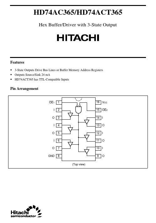
HD74AC365/HD74ACT365Hex Buffer/Driver with 3-State OutputFeatures• 3-State Outputs Drive Bus Lines or Buffer Memory Address Registers• Outputs Source/Sink 24 mA• HD74ACT365 has TTL-Compatible InputsPin ArrangementHD74AC365/HD74ACT3652Logic SymbolPin NamesOE 1, OE 23-State Output: Enable Input (Active Low)I Inputs OOutputsTruth TableInputs Output OE 1OE 2I O L L L L L L H H X H X Z H XXZH :High Voltage Level L :Low Voltage Level X :ImmaterialZ:High ImpedanceDC Characteristics (unless otherwise specified)ItemSymbol Max Unit ConditionMaximum quiescent supply current I CC 80µA V IN = V CC or ground, V CC = 5.5 V,Ta = Worst caseMaximum quiescent supply current I CC 8.0µA V IN = V CC or ground, V CC = 5.5 V,Ta = 25°CMaximum I CC /input (HD74ACT365)I CCT1.5mAV IN = V CC – 2.1 V, V CC = 5.5 V,Ta = Worst caseHD74AC365/HD74ACT3653AC Characteristics: HD74AC365Ta = +25°C C L = 50 pFTa = –40°C to +85°C C L = 50 pF ItemSymbol V CC (V)*1Min Typ Max Min Max Unit Propagation delay t PLH 3.3 1.07.09.0 1.010.0ns5.0 1.0 5.07.0 1.07.5Propagation delay t PHL 3.3 1.07.09.0 1.010.0ns 5.0 1.0 5.07.0 1.07.5Enable time t PZH 3.3 1.09.012.5 1.013.0ns 5.0 1.07.09.0 1.09.5Enable time t PZL 3.3 1.010.012.5 1.013.5ns 5.0 1.08.010.0 1.010.5Disable time t PHZ 3.3 1.09.512.0 1.012.5ns 5.0 1.07.510.0 1.010.5Disable time t PLZ3.3 1.09.012.5 1.013.5ns 5.01.07.010.01.010.5Note:1.Voltage Range 3.3 is 3.3 V ± 0.3 VVoltage Range 5.0 is 5.0 V ± 0.5 VAC Characteristics: HD74ACT365Ta = +25°C C L = 50 pFTa = –40°C to +85°C C L = 50 pF ItemSymbol V CC (V)*1Min Typ Max Min Max Unit Propagation delay t PLH 5.0 1.0 6.59.0 1.010.0ns Propagation delay t PHL 5.0 1.0 6.59.0 1.010.0ns Enable time t PZH 5.0 1.08.010.5 1.011.0ns Enable time t PZL 5.0 1.09.512.0 1.013.0ns Disable time t PHZ 5.0 1.09.512.0 1.013.0ns Disable time t PLZ5.01.08.010.51.011.5nsNote:1.Voltage Range 5.0 is 5.0 V ± 0.5 VCapacitanceItemSymbol Typ Unit Condition Input capacitanceC IN 4.5pF V CC = 5.5 V Power dissipation capacitanceC PD45.0pFV CC = 5.0 VHitachi CodeJEDECEIAJWeight (reference value)DP-16 Conforms Conforms 1.07 gHitachi Code JEDEC EIAJWeight (reference value)FP-16DA —Conforms 0.24 g*Dimension including the plating thicknessBase material dimension° – 8°Hitachi CodeJEDECEIAJWeight (reference value)FP-16DN Conforms Conforms 0.15 g*Dimension including the plating thickness Base material dimension° – 8°Hitachi CodeJEDECEIAJWeight (reference value)TTP-16DA ——0.05 g*Dimension including the plating thickness Base material dimensionCautions1.Hitachi neither warrants nor grants licenses of any rights of Hitachi’s or any third party’s patent,copyright, trademark, or other intellectual property rights for information contained in this document.Hitachi bears no responsibility for problems that may arise with third party’s rights, includingintellectual property rights, in connection with use of the information contained in this document.2.Products and product specifications may be subject to change without notice. Confirm that you have received the latest product standards or specifications before final design, purchase or use.3.Hitachi makes every attempt to ensure that its products are of high quality and reliability. However,contact Hitachi’s sales office before using the product in an application that demands especially high quality and reliability or where its failure or malfunction may directly threaten human life or cause risk of bodily injury, such as aerospace, aeronautics, nuclear power, combustion control, transportation,traffic, safety equipment or medical equipment for life support.4.Design your application so that the product is used within the ranges guaranteed by Hitachi particularly for maximum rating, operating supply voltage range, heat radiation characteristics, installationconditions and other characteristics. Hitachi bears no responsibility for failure or damage when used beyond the guaranteed ranges. Even within the guaranteed ranges, consider normally foreseeable failure rates or failure modes in semiconductor devices and employ systemic measures such as fail-safes, so that the equipment incorporating Hitachi product does not cause bodily injury, fire or other consequential damage due to operation of the Hitachi product.5.This product is not designed to be radiation resistant.6.No one is permitted to reproduce or duplicate, in any form, the whole or part of this document without written approval from Hitachi.7.Contact Hitachi’s sales office for any questions regarding this document or Hitachi semiconductor products.Hitachi, Ltd.Semiconductor & Integrated Circuits.Nippon Bldg., 2-6-2, Ohte-machi, Chiyoda-ku, Tokyo 100-0004, Japan Tel: Tokyo (03) 3270-2111 Fax: (03) 3270-5109Copyright ' Hitachi, Ltd., 1999. All rights reserved. Printed in Japan.Hitachi Asia Pte. Ltd.16 Collyer Quay #20-00Hitachi TowerSingapore 049318Tel: 535-2100Fax: 535-1533URLNorthAmerica : http:/Europe : /hel/ecg Asia (Singapore): .sg/grp3/sicd/index.htm Asia (Taiwan): /E/Product/SICD_Frame.htm Asia (HongKong): /eng/bo/grp3/index.htm Japan : http://www.hitachi.co.jp/Sicd/indx.htmHitachi Asia Ltd.Taipei Branch Office3F, Hung Kuo Building. No.167, Tun-Hwa North Road, Taipei (105)Tel: <886> (2) 2718-3666Fax: <886> (2) 2718-8180Hitachi Asia (Hong Kong) Ltd.Group III (Electronic Components)7/F., North Tower, World Finance Centre,Harbour City, Canton Road, Tsim Sha Tsui,Kowloon, Hong Kong Tel: <852> (2) 735 9218Fax: <852> (2) 730 0281 Telex: 40815 HITEC HXHitachi Europe Ltd.Electronic Components Group.Whitebrook ParkLower Cookham Road MaidenheadBerkshire SL6 8YA, United Kingdom Tel: <44> (1628) 585000Fax: <44> (1628) 778322Hitachi Europe GmbHElectronic components Group Dornacher Stra§e 3D-85622 Feldkirchen, Munich GermanyTel: <49> (89) 9 9180-0Fax: <49> (89) 9 29 30 00Hitachi Semiconductor (America) Inc.179 East Tasman Drive,San Jose,CA 95134 Tel: <1> (408) 433-1990Fax: <1>(408) 433-0223For further information write to:。
CD74HCT4060M96G4,CD74HCT4060MG4,CD74HCT4060MTG4, 规格书,Datasheet 资料

Data sheet acquired from Harris Semiconductor SCHS207GFeatures•Onboard Oscillator•Common Reset•Negative-Edge Clocking•Fanout (Over Temperature Range)-Standard Outputs. . . . . . . . . . . . . . .10 LSTTL Loads -Bus Driver Outputs . . . . . . . . . . . . .15 LSTTL Loads •Wide Operating Temperature Range . . .-55o C to 125o C •Balanced Propagation Delay and Transition Times •Significant Power Reduction Compared to LSTTL Logic ICs •HC Types-2V to 6V Operation-High Noise Immunity: N IL = 30%, N IH = 30% of V CC at V CC = 5V •HCT Types- 4.5V to 5.5V Operation-Direct LSTTL Input Logic Compatibility,V IL = 0.8V (Max), V IH = 2V (Min)-CMOS Input Compatibility, I l ≤1µA at V OL , V OHDescriptionThe ’HC4060and ’HCT4060each consist of an oscillator section and 14ripple-carry binary counter stages.The oscillator configuration allows design of either RC or crystal oscillator circuits.A Master Reset input is provided which resets the counter to the all-0’s state and disables the oscillator.A high level on the MR line accomplishes the reset function.All counter stages are master-slave flip-flops.The state of the counter is advanced one step in binary order onthe negative transition of φI (and φO).All inputs and outputs are buffered.Schmitt trigger action on the input-pulse-line permits unlimited rise and fall times.In order to achieve a symmetrical waveform in the oscillator section the HCT4060input pulse switch points are the same as in the HC4060;only the MR input in the HCT4060has TTL switching levels.PinoutCD54HC4060, CD54HCT4060 (CERDIP)CD74HC4060 (PDIP, SOIC, TSSOP)CD74HCT4060 (PDIP, SOIC)TOP VIEWOrdering InformationPART NUMBER TEMP. RANGE(o C)PACKAGE CD54HC4060F3A -55 to 12516 Ld CERDIP CD54HCT4060F3A -55 to 12516 Ld CERDIP CD74HC4060E -55 to 12516 Ld PDIP CD74HC4060M -55 to 12516 Ld SOIC CD74HC4060MT -55 to 12516 Ld SOIC CD74HC4060M96-55 to 12516 Ld SOIC CD74HC4060PW -55 to 12516 Ld TSSOP CD74HC4060PWR -55 to 12516 Ld TSSOP CD74HC4060PWT -55 to 12516 Ld TSSOP CD74HCT4060E -55 to 12516 Ld PDIP CD74HCT4060M -55 to 12516 Ld SOIC CD74HCT4060MT -55 to 12516 Ld SOIC CD74HCT4060M96-55 to 12516 Ld SOICNOTE:When ordering,use the entire part number.The suffixes 96and R denote tape and reel.The suffix T denotes a small-quantity reel of 250.14151691312111012345768Q12Q13Q14Q6Q5Q7GND Q4V CC Q8Q9MR φI φO φOQ10February 1998 - Revised October 2003CAUTION: These devices are sensitive to electrostatic discharge. Users should follow proper IC Handling Procedures.CD54HC4060, CD74HC4060,CD54HCT4060, CD74HCT4060High-Speed CMOS Logic14-Stage Binary Counter with Oscillator[ /Title (CD74HC4060,CD74HCT4060)/Sub-ject (High Speed CMOSFunctional DiagramφIQ4Q5Q6Q7Q9Q12Q14φO φOMRQ13Q10Q814-STAGE RIPPLE COUNTER ANDOSCILLATORGND = 8V CC = 1675461313215141211910FIGURE 1.LOGIC BLOCK DIAGRAMTRUTH TABLEøIMR OUTPUT STATE ↑L No Change ↓L Advance to Next State XHAll Outputs are Lowø1Q1FF1ø1Q1Rø4Q4FF4ø4Q4Rø14Q14FF14ø14Q14Rø5Q13FF5 - FF13ø5Q13R7235, 4, 6, 14, 13, 15, 1Q5 - Q10, Q12MR1211109Q14Q13Q4øO øO ø1Absolute Maximum Ratings Thermal InformationDC Supply Voltage, V CC. . . . . . . . . . . . . . . . . . . . . . . .-0.5V to 7V DC Input Diode Current, I IKFor V I < -0.5V or V I > V CC + 0.5V. . . . . . . . . . . . . . . . . . . . . .±20mA DC Output Diode Current, I OKFor V O < -0.5V or V O > V CC + 0.5V . . . . . . . . . . . . . . . . . . . .±20mA DC Drain Current, per Output, I OFor -0.5V < V O < V CC + 0.5V. . . . . . . . . . . . . . . . . . . . . . . . . .±25mA DC V CC or Ground Current, I CC . . . . . . . . . . . . . . . . . . . . . . . . .±50mA Operating ConditionsTemperature Range, T A . . . . . . . . . . . . . . . . . . . . . .-55o C to 125o C Supply Voltage Range, V CCHC T ypes . . . . . . . . . . . . . . . . . . . . . . . . . . . . . . . . . . . . .2V to 6V HCT T ypes . . . . . . . . . . . . . . . . . . . . . . . . . . . . . . . . .4.5V to 5.5V DC Input or Output Voltage, V I, V O . . . . . . . . . . . . . . . . .0V to V CC Input Rise and Fall Time2V . . . . . . . . . . . . . . . . . . . . . . . . . . . . . . . . . . . . . .1000ns (Max) 4.5V. . . . . . . . . . . . . . . . . . . . . . . . . . . . . . . . . . . . . .500ns (Max) 6V . . . . . . . . . . . . . . . . . . . . . . . . . . . . . . . . . . . . . . .400ns (Max)Thermal Resistance (T ypical, Note 1)θJA (o C/W) E (PDIP) Package . . . . . . . . . . . . . . . . . . . . . . . . . .67M (SOIC) Package. . . . . . . . . . . . . . . . . . . . . . . . . .73PW (TSSOP) Package . . . . . . . . . . . . . . . . . . . . . .108 Maximum Junction T emperature. . . . . . . . . . . . . . . . . . . . . . .150o C Maximum Storage Temperature Range . . . . . . . . . .-65o C to 150o C Maximum Lead T emperature (Soldering 10s). . . . . . . . . . . . .300o C (SOIC - Lead Tips Only)CAUTION:Stresses above those listed in“Absolute Maximum Ratings”may cause permanent damage to the device.This is a stress only rating and operation of the device at these or any other conditions above those indicated in the operational sections of this specification is not implied.NOTE:1.The package thermal impedance is calculated in accordance with JESD 51-7.DC Electrical SpecificationsPARAMETER SYMBOLTESTCONDITIONS VCC(V)25o C-40o C TO 85o C-55o C TO125o CUNITS V I(V)I O(mA)MIN TYP MAX MIN MAX MIN MAXHC TYPESHigh Level Input Voltage V IH--2 1.5-- 1.5- 1.5-V4.5 3.15-- 3.15 - 3.15-V6 4.2-- 4.2- 4.2-VLow Level Input Voltage V IL--2--0.5-0.5-0.5V4.5-- 1.35- 1.35- 1.35V6-- 1.8- 1.8- 1.8VHigh Level Output Voltage Q Outputs CMOS Loads V OH V IH or V IL-0.022 1.9-- 1.9- 1.9-V -0.02 4.5 4.4-- 4.4 - 4.4-V-0.026 5.9-- 5.9- 5.9-VHigh Level Output Voltage Q Outputs TTL Loads---------V -4 4.5 3.98-- 3.84- 3.7-V -5.26 5.48-- 5.34- 5.2-VLow Level Output Voltage Q Outputs CMOS Loads V OL V IH or V IL0.022--0.1-0.1-0.1V0.02 4.5--0.1-0.1-0.1V0.026--0.1-0.1-0.1VLow Level Output Voltage Q Outputs TTL Loads---------V4 4.5--0.26-0.33-0.4V5.26--0.26-0.33-0.4VHigh-Level Output VoltageφO Output (Pin 10)CMOS Loads V OH V CC orGND-0.022 1.9-- 1.9- 1.9-V-0.02 4.5 4.4-- 4.4- 4.4-V-0.026 5.9-- 5.9- 5.9-VHigh-Level Output VoltageφO Output (Pin 10)TTL Loads (Note 2)V OH V CC orGND-2.6 4.5 3.98-- 3.84- 3.7-V-3.36 5.48-- 5.34- 5.2-VLow-Level Output VoltageφO Output (Pin 10)CMOS Loads V OL V CC orGND0.022--0.1-0.1-0.1V0.02 4.5--0.1-0.1-0.1V0.026--0.1-0.1-0.1VLow-Level Output VoltageφO Output (Pin 10)TTL Loads V OL V CC orGND2.6 4.5--0.26-0.33-0.4V3.36--0.26-0.33-0.4VHigh-Level Output VoltageφO Output (Pin 9)TTL Loads V OH V IL or V IH-3.2 4.5 3.98-- 3.84- 3.7-V -4.26 5.48-- 5.34- 5.2-VLow-Level Output VoltageφO Output (Pin 9)TTL Loads V OL V IL or V IH-2.6 4.5--0.26-0.33-0.4V -3.36--0.26-0.33-0.4VInput Leakage Current I I V CC orGND-6--±0.1-±1-±1µAQuiescent Device Current I CC V CC orGND06--8-80-160µAHCT TYPESHigh Level Input Voltage V IH-- 4.5 to5.52--2-2-VLow Level Input Voltage V IL-- 4.5 to5.5--0.8-0.8-0.8VHigh Level Output Voltage Q Outputs CMOS Loads V OH V IH or V IL(Note 3)-0.02 4.5 4.4-- 4.4- 4.4-VHigh Level OutputVoltage Q OutputsTTL Loads-4 4.5 3.98-- 3.84- 3.7-VLow Level Output Voltage Q Outputs CMOS Loads V OL V IH or V IL(Note 3)0.02 4.5--0.1-0.1-0.1VLow Level OutputVoltage Q OutputsTTL Loads4 4.5--0.26-0.33-0.4VHigh-Level Output VoltageφO Output (Pin 10)CMOS Loads V OH V CC orGND-0.02 4.5 4.4-- 4.4- 4.4-VHigh-Level Output VoltageφO Output (Pin 10)TTL Loads (Note 2)V OH V CC orGND-2.6 4.5 3.98-- 3.84- 3.7-VLow-Level Output VoltageφO Output (Pin 10)CMOS Loads V OL V CC orGND0.02 4.5--0.1-0.1-0.1VPARAMETER SYMBOLCONDITIONS VCC(V)25o C-40o C TO 85o C-55o C TO125o CUNITS V I(V)I O(mA)MIN TYP MAX MIN MAX MIN MAXLow-Level Output Voltage φO Output (Pin 10)TTL Loads V OLV CC or GND2.64.5--0.26-0.33-0.4VHigh-Level Output Voltage φO Output (Pin 9)TTL Loads V OH V IL or V IH-3.2 4.5 3.98-- 3.84- 3.7-VLow-Level Output Voltage φO Output (Pin 9)TTL Loads V OLV IH or V IL (Note 3)3.24.5-0.26-0.33-0.4VInput Leakage CurrentI IAny Voltage Between V CC and GND - 5.5-±0.1-±1-±1µAQuiescent Device CurrentI CC V CC or GND 0 5.5--8-80-160µA Additional Quiescent Device Current Per Input Pin: 1 Unit Load ∆I CC (Note 4)V CC - 2.1-4.5 to5.5-100360-450-490µANOTES:2.Limits not valid when pin 12 (instead of pin 11) is used as control input.3.For pin 11 V IH = 3.15V, V IL = 0.9V.4.For dual-supply systems theoretical worst case (V I = 2.4V, V CC =5.5V) specification is 1.8mA.PARAMETER SYMBOL CONDITIONSV CC (V)25o C-40o C TO 85o C -55o C TO 125o C UNITS V I (V)I O (mA)MIN TYP MAX MIN MAX MIN MAX HCT Input Loading TableINPUT UNIT LOADSMR0.35NOTE:Unit Load is ∆I CC limit specified in DC Electrical Specifica-tions Table, e.g. 360µA max at 25o C.Prerequisite for Switching SpecificationsPARAMETER SYMBOLV CC (V)25o C-40o C TO 85o C -55o C TO 125o C UNITSMINTYPMAXMINTYPMAXMINTYPMAXHC TYPESMaximum Input Pulse Frequencyf max26--5--4--MHz 4.530--25--20--MHz 635--29--23--MHz Input Pulse Widtht W280--100--120--ns 4.516--20--24--ns 614--17--20--ns Reset Removal Timet REM2100--125--150--ns 4.520--25--30--ns 617--21--26--nsReset Pulse Widtht W280--100--120--ns 4.516--20--24--ns 614--17--20--ns HCT TYPES Maximum Input,Pulse Frequency f max 4.530--25--20--MHz Input Pulse Width t W 4.516--20--24--ns Reset Removal Time t REM 4.526--33--39--ns Reset Pulse Widtht W4.525--31--38--nsPrerequisite for Switching Specifications(Continued)PARAMETER SYMBOLV CC (V)25o C -40o C TO 85o C -55o C TO 125o C UNITS MIN TYP MAX MIN TYP MAX MIN TYP MAX Switching SpecificationsInput t r , t f = 6nsPARAMETERSYMBOLTEST CONDITIONSV CC (V)25o C-40o C TO 85o C -55o C TO 125o C UNITSMINTYPMAXMINMAXMINMAXHC TYPES Propagation Delayt PLH , t PHLC L = 50pF2--300-375-450ns φI to Q44.5--60-75-90ns C L = 15pF 5-25-----ns C L = 50pF6--51-64-78ns Q n to Q n+1t PLH , t PHLC L = 50pF2--80-100-120ns 4.5--16-20-24ns C L = 15pF 5-6-----ns C L = 50pF6--14-17-20ns MR to Q nt PHLC L = 50pF2--175-220-265ns 4.5--35-44-53ns C L = 15pF 5-14-----ns C L = 50pF6--30-37-45ns Output Transition Timet THL , t TLHC L = 50pF2--75-95-110ns 4.5--15-19-22ns 6--13-16-19nsInput Capacitance C I (TBD)Propagation Dissipation Capacitance (Notes 5, 6)C PD---40-----pFHCT TYPES Propagation Delayt PLH , t PHLC L = 50pF2--------ns φI to Q44.5--66-83-100ns C L = 15pF 5-25------ns C L = 50pF6--------nsQ n to Q n+1t PLH , t PHLC L = 50pF2-------ns 4.5--16-20-24ns C L = 15pF 5-6-----ns C L = 50pF6-------ns MR to Q nt PHLC L = 50pF2-------ns 4.5--44-55-66ns C L = 15pF 5-17-----ns C L = 50pF6-------ns Output Transition Timet THL , t TLHC L = 50pF2-------ns 4.5--15-19-22ns 6-------nsInput Capacitance C I (TBD)Propagation Dissipation Capacitance (Notes 5, 6)C PD---40-----pFNOTES:5.C PD is used to determine the dynamic power consumption, per package.6.P D = C PD V CC 2 f i ∑(C L V CC 2 f i /M) where M = 21, 22, 23, ...214, f i =input frequency, C L = output load capacitance.Switching SpecificationsInput t r , t f = 6ns (Continued)PARAMETER SYMBOL TEST CONDITIONS V CC (V)25o C-40o C TO 85o C -55o C TO 125o C UNITS MIN TYP MAX MIN MAX MIN MAX TYPICAL LIMIT VALUES FOR R X AND C XPARAMETER TEST CONDITIONS VOLTAGETYPICAL MAXIMUM LIMITS R X MinimumC X > 1000pF 21K ΩC X > 10pF 4.5C X > 10pF6R X MaximumC X > 10pF 220M ΩC X > 10pF 4.5C X > 10pF6C X MinimumR X > 10K Ω210pFR X > 10K Ω 4.5R X > 10K Ω6R X = 1K Ω21000pF R X = 1K Ω 4.510pF R X = 1K Ω610pF MaximumAstable Oscillator FrequencyC X = 1000pF,R X = 1K Ω20.5MHz (Note 7)C X = 100pF,R X = 1K Ω 4.53MHz (Note 7)C X = 100pF,R X = 1K Ω63MHz (Note 7)NOTE:7.At very high frequencies f =1/2.2R X C X no longer gives an accurate approximation.NOTE:OSC Frequency ≈ 1/2.2 R X C XFor 1M Ω > R X > 1K Ω, C X > 10pF , f < 1MHzFIGURE 2.FREQUENCY OF ON-BOARD OSCILLATOR AS AFUNCTION OF C X AND R X10210110-110-210-310-410-510-110010102103104105106OSCILLATOR FREQUENCY (Hz)C X (µF )T A = 25o C R X = 1K Ω10K Ω100K Ω1M Ω10M ΩCD54/74HC4060, CD54/74HCT4060Typical Performance CurvesNOTE:Outputs should be switching from 10% V CC to 90% V CC in accordance with device truth table.For f MAX ,input duty cycle =50%.FIGURE 3.HC CLOCK PULSE RISE AND FALL TIMES ANDPULSE WIDTHNOTE:Outputs should be switching from 10% V CC to 90% V CC in accordance with device truth table.For f MAX ,input duty cycle =50%.FIGURE 4.HCT CLOCK PULSE RISE AND FALL TIMES ANDPULSE WIDTHFIGURE 5.HC AND HCT TRANSITION TIMES AND PROPAGA-TION DELAY TIMES, COMBINATION LOGIC FIGURE 6.HCT TRANSITION TIMES AND PROPAGATIONDELAY TIMES, COMBINATION LOGICCLOCK90%50%10%GNDV CCt r C L t f C L 50%50%t WLt WH10%t WL + t WH =fC LICLOCK 2.7V 1.3V0.3VGND3Vt r C L = 6nst f C L = 6ns1.3V 1.3V t WLt WH0.3V t WL + t WH =fC L I t PHLt PLHt THL t TLH 90%50%10%50%10%INVERTING OUTPUT INPUTGNDV CCt r = 6nst f = 6ns90%t PHLt PLHt THLt TLH 2.7V 1.3V 0.3V1.3V 10%INVERTING OUTPUTINPUTGND 3Vt r = 6nst f = 6ns90%CD54/74HC4060, CD54/74HCT4060Addendum-Page 1PACKAGING INFORMATIONOrderable Device Status(1)Package Type PackageDrawingPins Package QtyEco Plan(2)Lead/Ball Finish MSL Peak Temp (3)Samples (Requires Login)5962-8768001EA ACTIVE CDIP J 161TBD Call TI Call TI 5962-8977101EA ACTIVE CDIP J 161TBD Call TI Call TICD54HC4060F3A ACTIVE CDIP J 161TBD A42N / A for Pkg Type CD54HCT4060F3A ACTIVE CDIP J 161TBDA42N / A for Pkg TypeCD74HC4060E ACTIVE PDIP N 1625Pb-Free (RoHS)CU NIPDAU N / A for Pkg Type CD74HC4060EE4ACTIVE PDIP N 1625Pb-Free (RoHS)CU NIPDAU N / A for Pkg Type CD74HC4060M ACTIVE SOIC D 1640Green (RoHS & no Sb/Br)CU NIPDAU Level-1-260C-UNLIM CD74HC4060M96ACTIVE SOIC D 162500Green (RoHS & no Sb/Br)CU NIPDAU Level-1-260C-UNLIM CD74HC4060M96E4ACTIVE SOIC D 162500Green (RoHS & no Sb/Br)CU NIPDAU Level-1-260C-UNLIM CD74HC4060M96G4ACTIVE SOIC D 162500Green (RoHS & no Sb/Br)CU NIPDAU Level-1-260C-UNLIM CD74HC4060ME4ACTIVE SOIC D 1640Green (RoHS & no Sb/Br)CU NIPDAU Level-1-260C-UNLIM CD74HC4060MG4ACTIVE SOIC D 1640Green (RoHS & no Sb/Br)CU NIPDAU Level-1-260C-UNLIM CD74HC4060MT ACTIVE SOIC D 16250Green (RoHS & no Sb/Br)CU NIPDAU Level-1-260C-UNLIM CD74HC4060MTE4ACTIVE SOIC D 16250Green (RoHS & no Sb/Br)CU NIPDAU Level-1-260C-UNLIM CD74HC4060MTG4ACTIVE SOIC D 16250Green (RoHS & no Sb/Br)CU NIPDAU Level-1-260C-UNLIM CD74HC4060PW ACTIVE TSSOP PW 1690Green (RoHS & no Sb/Br)CU NIPDAU Level-1-260C-UNLIM CD74HC4060PWE4ACTIVE TSSOP PW 1690Green (RoHS & no Sb/Br)CU NIPDAU Level-1-260C-UNLIM CD74HC4060PWG4ACTIVE TSSOP PW 1690Green (RoHS & no Sb/Br)CU NIPDAU Level-1-260C-UNLIM CD74HC4060PWRACTIVETSSOPPW162000Green (RoHS & no Sb/Br)CU NIPDAU Level-1-260C-UNLIM芯天下--/Addendum-Page 2Orderable Device Status(1)Package Type PackageDrawingPins Package QtyEco Plan(2)Lead/Ball FinishMSL Peak Temp(3)Samples (Requires Login)CD74HC4060PWRE4ACTIVE TSSOP PW 162000Green (RoHS & no Sb/Br)CU NIPDAU Level-1-260C-UNLIM CD74HC4060PWRG4ACTIVE TSSOP PW 162000Green (RoHS & no Sb/Br)CU NIPDAU Level-1-260C-UNLIM CD74HC4060PWT ACTIVE TSSOP PW 16250Green (RoHS & no Sb/Br)CU NIPDAU Level-1-260C-UNLIM CD74HC4060PWTE4ACTIVE TSSOP PW 16250Green (RoHS & no Sb/Br)CU NIPDAU Level-1-260C-UNLIM CD74HC4060PWTG4ACTIVE TSSOP PW 16250Green (RoHS & no Sb/Br)CU NIPDAU Level-1-260C-UNLIM CD74HCT4060E ACTIVE PDIP N 1625Pb-Free (RoHS)CU NIPDAU N / A for Pkg Type CD74HCT4060EE4ACTIVE PDIP N 1625Pb-Free (RoHS)CU NIPDAU N / A for Pkg Type CD74HCT4060M ACTIVE SOIC D 1640Green (RoHS & no Sb/Br)CU NIPDAU Level-1-260C-UNLIM CD74HCT4060M96ACTIVE SOIC D 162500Green (RoHS & no Sb/Br)CU NIPDAU Level-1-260C-UNLIM CD74HCT4060M96E4ACTIVE SOIC D 162500Green (RoHS & no Sb/Br)CU NIPDAU Level-1-260C-UNLIM CD74HCT4060M96G4ACTIVE SOIC D 162500Green (RoHS & no Sb/Br)CU NIPDAU Level-1-260C-UNLIM CD74HCT4060ME4ACTIVE SOIC D 1640Green (RoHS & no Sb/Br)CU NIPDAU Level-1-260C-UNLIM CD74HCT4060MG4ACTIVE SOIC D 1640Green (RoHS & no Sb/Br)CU NIPDAU Level-1-260C-UNLIM CD74HCT4060MT ACTIVE SOIC D 16250Green (RoHS & no Sb/Br)CU NIPDAU Level-1-260C-UNLIM CD74HCT4060MTE4ACTIVE SOIC D 16250Green (RoHS & no Sb/Br)CU NIPDAU Level-1-260C-UNLIM CD74HCT4060MTG4ACTIVESOICD16250Green (RoHS & no Sb/Br)CU NIPDAU Level-1-260C-UNLIM(1)The marketing status values are defined as follows:ACTIVE: Product device recommended for new designs.LIFEBUY: TI has announced that the device will be discontinued, and a lifetime-buy period is in effect.NRND: Not recommended for new designs. Device is in production to support existing customers, but TI does not recommend using this part in a new design.PREVIEW: Device has been announced but is not in production. Samples may or may not be available.OBSOLETE: TI has discontinued the production of the device.芯天下--/PACKAGE OPTION ADDENDUM5-Sep-2011Addendum-Page 3(2)Eco Plan - The planned eco-friendly classification: Pb-Free (RoHS), Pb-Free (RoHS Exempt), or Green (RoHS & no Sb/Br) - please check /productcontent for the latest availability information and additional product content details.TBD: The Pb-Free/Green conversion plan has not been defined.Pb-Free (RoHS): TI's terms "Lead-Free" or "Pb-Free" mean semiconductor products that are compatible with the current RoHS requirements for all 6 substances, including the requirement that lead not exceed 0.1% by weight in homogeneous materials. Where designed to be soldered at high temperatures, TI Pb-Free products are suitable for use in specified lead-free processes.Pb-Free (RoHS Exempt): This component has a RoHS exemption for either 1) lead-based flip-chip solder bumps used between the die and package, or 2) lead-based die adhesive used between the die and leadframe. The component is otherwise considered Pb-Free (RoHS compatible) as defined above.Green (RoHS & no Sb/Br): TI defines "Green" to mean Pb-Free (RoHS compatible), and free of Bromine (Br) and Antimony (Sb) based flame retardants (Br or Sb do not exceed 0.1% by weight in homogeneous material)(3)MSL, Peak Temp. -- The Moisture Sensitivity Level rating according to the JEDEC industry standard classifications, and peak solder temperature.Important Information and Disclaimer:The information provided on this page represents TI's knowledge and belief as of the date that it is provided. TI bases its knowledge and belief on information provided by third parties, and makes no representation or warranty as to the accuracy of such information. Efforts are underway to better integrate information from third parties. TI has taken and continues to take reasonable steps to provide representative and accurate information but may not have conducted destructive testing or chemical analysis on incoming materials and chemicals.TI and TI suppliers consider certain information to be proprietary, and thus CAS numbers and other limited information may not be available for release.In no event shall TI's liability arising out of such information exceed the total purchase price of the TI part(s) at issue in this document sold by TI to Customer on an annual basis.OTHER QUALIFIED VERSIONS OF CD54HC4060, CD54HCT4060, CD74HC4060, CD74HCT4060 :•Catalog: CD74HC4060, CD74HCT4060•Military: CD54HC4060, CD54HCT4060NOTE: Qualified Version Definitions:•Catalog - TI's standard catalog product•Military - QML certified for Military and Defense Applications芯天下--/TAPE AND REELINFORMATION*All dimensionsare nominalDevicePackage Type Package Drawing Pins SPQReel Diameter (mm)Reel Width W1(mm)A0(mm)B0(mm)K0(mm)P1(mm)W (mm)Pin1Quadrant CD74HC4060M96SOIC D 162500330.016.4 6.510.3 2.18.016.0Q1CD74HC4060PWR TSSOP PW 162000330.012.4 6.9 5.6 1.68.012.0Q1CD74HC4060PWT TSSOP PW 16250330.012.4 6.9 5.6 1.68.012.0Q1CD74HCT4060M96SOICD162500330.016.46.510.32.18.016.0Q114-Jul-2012*All dimensionsare nominalDevice Package TypePackage DrawingPins SPQ Length (mm)Width (mm)Height (mm)CD74HC4060M96SOIC D 162500333.2345.928.6CD74HC4060PWR TSSOP PW 162000367.0367.035.0CD74HC4060PWT TSSOP PW 16250367.0367.035.0CD74HCT4060M96SOICD162500333.2345.928.614-Jul-2012IMPORTANT NOTICETexas Instruments Incorporated and its subsidiaries(TI)reserve the right to make corrections,enhancements,improvements and other changes to its semiconductor products and services per JESD46C and to discontinue any product or service per JESD48B.Buyers should obtain the latest relevant information before placing orders and should verify that such information is current and complete.All semiconductor products(also referred to herein as“components”)are sold subject to TI’s terms and conditions of sale supplied at the time of order acknowledgment.TI warrants performance of its components to the specifications applicable at the time of sale,in accordance with the warranty in TI’s terms and conditions of sale of semiconductor products.Testing and other quality control techniques are used to the extent TI deems necessary to support this warranty.Except where mandated by applicable law,testing of all parameters of each component is not necessarily performed.TI assumes no liability for applications assistance or the design of Buyers’products.Buyers are responsible for their products and applications using TI components.To minimize the risks associated with Buyers’products and applications,Buyers should provide adequate design and operating safeguards.TI does not warrant or represent that any license,either express or implied,is granted under any patent right,copyright,mask work right,or other intellectual property right relating to any combination,machine,or process in which TI components or services are rmation published by TI regarding third-party products or services does not constitute a license to use such products or services or a warranty or endorsement e of such information may require a license from a third party under the patents or other intellectual property of the third party,or a license from TI under the patents or other intellectual property of TI.Reproduction of significant portions of TI information in TI data books or data sheets is permissible only if reproduction is without alteration and is accompanied by all associated warranties,conditions,limitations,and notices.TI is not responsible or liable for such altered rmation of third parties may be subject to additional restrictions.Resale of TI components or services with statements different from or beyond the parameters stated by TI for that component or service voids all express and any implied warranties for the associated TI component or service and is an unfair and deceptive business practice. TI is not responsible or liable for any such statements.Buyer acknowledges and agrees that it is solely responsible for compliance with all legal,regulatory and safety-related requirements concerning its products,and any use of TI components in its applications,notwithstanding any applications-related information or support that may be provided by TI.Buyer represents and agrees that it has all the necessary expertise to create and implement safeguards which anticipate dangerous consequences of failures,monitor failures and their consequences,lessen the likelihood of failures that might cause harm and take appropriate remedial actions.Buyer will fully indemnify TI and its representatives against any damages arising out of the use of any TI components in safety-critical applications.In some cases,TI components may be promoted specifically to facilitate safety-related applications.With such components,TI’s goal is to help enable customers to design and create their own end-product solutions that meet applicable functional safety standards and requirements.Nonetheless,such components are subject to these terms.No TI components are authorized for use in FDA Class III(or similar life-critical medical equipment)unless authorized officers of the parties have executed a special agreement specifically governing such use.Only those TI components which TI has specifically designated as military grade or“enhanced plastic”are designed and intended for use in military/aerospace applications or environments.Buyer acknowledges and agrees that any military or aerospace use of TI components which have not been so designated is solely at the Buyer's risk,and that Buyer is solely responsible for compliance with all legal and regulatory requirements in connection with such use.TI has specifically designated certain components which meet ISO/TS16949requirements,mainly for automotive ponents which have not been so designated are neither designed nor intended for automotive use;and TI will not be responsible for any failure of such components to meet such requirements.Products ApplicationsAudio /audio Automotive and Transportation /automotiveAmplifiers Communications and Telecom /communicationsData Converters Computers and Peripherals /computersDLP®Products Consumer Electronics /consumer-appsDSP Energy and Lighting /energyClocks and Timers /clocks Industrial /industrialInterface Medical /medicalLogic Security /securityPower Mgmt Space,Avionics and Defense /space-avionics-defense Microcontrollers Video and Imaging /videoRFID OMAP Mobile Processors /omap TI E2E Community Wireless Connectivity /wirelessconnectivityMailing Address:Texas Instruments,Post Office Box655303,Dallas,Texas75265Copyright©2012,Texas Instruments Incorporated。
FD270中文资料
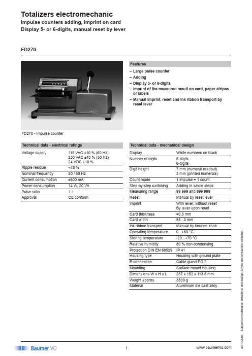
Totalizers electromechanicS u b j e c t t o m o d i fi c a t i o n i n t e c h n i c a n d d e s i g n . E r r o r s a n d o m i s s i o n s e x c e p t e d .008FD270 - Impulse counterFeaturesLarge pulse counter –Adding–Display 5- or 6-digits–Imprint of the measured result on card, paper stripes –or labelsManual imprint, reset and ink ribbon transport by –reset leverTechnical data - electrical ratings Voltage supply115 VAC ±10 % (60 Hz) 230 VAC ±10 % (50 Hz) 24 VDC ±10 %Ripple residue <48 %Nominal frequency 50 / 60 Hz Current consumption ≤600 mA Power consumption 14 W, 20 VA Pulse ratio 1:1ApprovalCE conformFD270Technical data - mechanical design DisplayWhite numbers on black Number of digits 5-digits 6-digitsDigit height7 mm (numeral readout) 3 mm (printed numerals)Count mode1 impulse = 1 count Step-by-step switching Adding in whole steps Measuring range 99 999 and 999 999Reset Manual by reset lever Imprint With lever, without reset By lever upon reset Card thickness ≤0.3 mm Card width 85...0 mmInk ribbon transport Manual by knurled knob Operating temperature 0...+60 °C Storing temperature -20...+70 °CRelative humidity 80 % non-condensing Protection DIN EN 60529IP 41Housing type Housing with ground plate E-connection Cable gland PG 9 MountingSurface mount housing Dimensions W x H x L 237 x 152 x 113.5 mm Weight approx.3500 gMaterialAluminium die cast alloyImpulse counters adding, imprint on card Display 5- or 6-digits, manual reset by leverTotalizers electromechanicS u b j e c t t o m o d i fi c a t i o n i n t e c h n i c a n d d e s i g n . E r r o r s a n d o m i s s i o n s e x c e p t e d .008FD270Part number FD270.DisplayA55-digits 9999.9 A75-digits 99999 C16-digits 999 999B76-digits 99999.5,count mode 0-5-0-5Voltage 124 VDC5115 VAC / 60 Hz 6230 VAC / 50 HzImprint / reset010A Imprint and reset operation parallel020CImprint and reset operation separateImpulse counters adding, imprint on card Display 5- or 6-digits, manual reset by leverConnection diagramDimensionsVoltage 24 VDC ±10 %Power14 W Nominal current 600 mA Resistance 38 ΩVoltage 115 VAC ±10 %Power20 VA Nominal current 180 mA Resistance 50 ΩVoltage 230 VAC +6/-10 %Power20 VA Nominal current 80 mA Resistance290 ΩTrigger level。
74F579中文资料

元器件交易网DIP20:plastic dual in-line package; 20 leads (300 mil)SOT146-1SO20:plastic small outline package; 20 leads; body width 7.5 mm SOT163-1NOTESDefinitionsShort-form specification — The data in a short-form specification is extracted from a full data sheet with the same type number and title. For detailed information see the relevant data sheet or data handbook.Limiting values definition — Limiting values given are in accordance with the Absolute Maximum Rating System (IEC 134). Stress above one or more of the limiting values may cause permanent damage to the device. These are stress ratings only and operation of the device at these or at any other conditions above those given in the Characteristics sections of the specification is not implied. Exposure to limiting values for extended periods may affect device reliability.Application information — Applications that are described herein for any of these products are for illustrative purposes only. Philips Semiconductors make no representation or warranty that such applications will be suitable for the specified use without further testing or modification.DisclaimersLife support — These products are not designed for use in life support appliances, devices or systems where malfunction of these products can reasonably be expected to result in personal injury. Philips Semiconductors customers using or selling these products for use in such applications do so at their own risk and agree to fully indemnify Philips Semiconductors for any damages resulting from such application.Right to make changes — Philips Semiconductors reserves the right to make changes, without notice, in the products, including circuits, standard cells, and/or software, described or contained herein in order to improve design and/or performance. Philips Semiconductors assumes no responsibility or liability for the use of any of these products, conveys no license or title under any patent, copyright, or mask work right to these products, and makes no representations or warranties that these products are free from patent, copyright, or mask work right infringement, unless otherwise specified.Philips Semiconductors811 East Arques AvenueP.O. Box 3409Sunnyvale, California 94088–3409Telephone 800-234-7381© Copyright Philips Electronics North America Corporation 1998All rights reserved. Printed in U.S.A.print code Date of release: 10-98。
MC74ACT257D中文资料
VIL
Guaranteed Limits 2.1 3.15 3.85 0.9 1.35 1.65 2.9 4.4 5.4 2.56 3.86 4.86 0.1 0.1 0.1 0.36 0.36 0.36 ±0.1 2.1 3.15 3.85 0.9 1.35 1.65 2.9 4.4 5.4 2.46 3.76 4.76 0.1 0.1 0.1 0.44 0.44 0.44 ±1.0 V VOUT = 0.1 V or VCC – 0.1 V VOUT = 0.1 V or VCC – 0.1 V IOUT = –50 µA V *VIN = VIL or VIH –12 mA IOH –24 mA –24 mA IOUT = 50 µA V *VIN = VIL or VIH 12 mA IOL 24 mA 24 mA VI = VCC, GND VI (OE) = VIL, VIH VI = VCC, GND VO = VCC, GND VOLD = 1.65 V Max VOHD = 3.85 V Min VIN = VCC or GND
FACT DATA 5-2
元器件交易网
MC74AC257 MC74ACT257
MAXIMUM RATINGS*
Symbol VCC Vin Vout Iin Iout ICC Tstg Parameter DC Supply Voltage (Referenced to GND) DC Input Voltage (Referenced to GND) DC Output Voltage (Referenced to GND) DC Input Current, per Pin DC Output Sink/Source Current, per Pin DC VCC or GND Current per Output Pin Storage Temperature Value –0.5 to +7.0 –0.5 to VCC +0.5 –0.5 to VCC +0.5 ±20 ±50 ±50 –65 to +150 Unit V V V mA mA mA °C
MC74LCX74中文资料
* Absolute maximum continuous ratings are those values beyond which damage to the device may occur. Exposure to these conditions or conditions beyond those indicated may adversely affect device reliability. Functional operation under absolute–maximum–rated conditions is not implied. 1. Output in HIGH or LOW State. IO absolute maximum rating must be observed.
DC ELECTRICAL CHARACTERISTICS
TA = –40°C to +85°C Symbol VIH VIL VOH Characteristic HIGH Level Input Voltage (Note 2.) LOW Level Input Voltage (Note 2.) HIGH Level Output Voltage Condition 2.7V ≤ VCC ≤ 3.6V 2.7V ≤ VCC ≤ 3.6V 2.7V ≤ VCC ≤ 3.6V; IOH = –100µA VCC = 2.7V; IOH = –12mA VCC = 3.0V; IOH = –18mA VCC = 3.0V; IOH = –24mA VOL LOW Level Output Voltage 2.7V ≤ VCC ≤ 3.6V; IOL = 100µA VCC = 2.7V; IOL= 12mA VCC = 3.0V; IOL = 16mA VCC = 3.0V; IOL = 24mA 2. These values of VI are used to test DC electrical characteristics only. VCC – 0.2 2.2 2.4 2.2 0.2 0.4 0.4 0.55 V Min 2.0 0.8 Max Unit V V V
MCT270中文资料

2001 Infineon Technologies Corp. • Optoelectronics Division • San Jose, CA www.infi/opto • 1-888-Infineon (1-888-463-4636)DESCRIPTIONThis data sheet presents five families of Infineon Industry Standard Single Channel Phototransistor Couplers. These families include the 4N25/26/27/28 types, the 4N35/36/37/38 couplers, the H11A1/A2/A3/A4/A5, the MCT2/2E, and MCT270/271/272/273/274/275/276/277 devices.Each optocoupler consists of Gallium Arsenide infra-red LED and a silicon NPN phototransistor.These couplers are Underwriters Laboratories (UL) listed to comply with a 5300 V RMS Isolation Test Voltage. This isolation performance is accomplished through Infineon double molding isolation manu-facturing process. Compliance to VDE 0884 partial discharge isola-tion specification is available for these families by ordering option 1. Phototransistor gain stability, in the presence of high isolation volt-ages, is insured by incorporating a TRansparent lOn Shield (TRIOS) ®on the phototransistor substrate. These isolation pro-cesses and the Infineon IS09001 Quality program results in the highest isolation performance available for a commercial plastic phototransistor optocoupler.The devices are available in lead formed configuration suitable for surface mounting and are available either on tape and reel, or in standard tube shipping containers.DEVICE TYPES Part No.CTR % Min.Part No.CTR % Min. 4N2520MCT2204N2620MCT2E 204N2710MCT270504N2810MCT27145–904N35100MCT27275–1504N36100MCT273125–2504N37100MCT274225–4004N3810MCT27570–90H11A150MCT27615–60H11A220MCT277100H11A320H11A410H11A530FEATURES•Interfaces with Common Logic Families •Input-output Coupling Capacitance < 0.5 pF •Industry Standard Dual-in-line 6-pin Package •Field Effect Stable by TRIOS ® •5300 V RMS Isolation Test Voltage••VDE #0884 Approval Available with Option 1APPLICATIONS•AC Mains Detection •Reed Relay Driving•Switch Mode Power Supply Feedback •Telephone Ring Detection •Logic Ground Isolation•Logic Coupling with High Frequency Noise RejectionNotes:Designing with data sheet is covered in Application Note 45.元器件交易网Maximum Ratings T A =25 ° C EmitterReverse Voltage..........................................................................................6.0 V Forward Current ........................................................................................60 mA Surge Current (t ≤ 10 µ s)...............................................................................2.5 A Power Dissipation...................................................................................100 mW DetectorCollector-Emitter Breakdown Voltage...........................................................70 V Emitter-Base Breakdown Voltage................................................................7.0 V Collector Current.......................................................................................50 mA Collector Current(t <1.0 ms)....................................................................100 mA Power Dissipation...................................................................................150 mW PackageIsolation Test Voltage..........................................................................5300 V RMS Creepage .............................................................................................. ≥ 7.0 mm Clearance ............................................................................................. ≥ 7.0 mm Isolation Thickness between Emitter and Detector............................... ≥ 0.4 mm Comparative Tracking Index per DIN IEC 112/VDE0303, part 1..................175Isolation ResistanceV IO =500 V , T A =25 ° C...............................................................................10 12 Ω V IO =500 V , T A =100 ° C............................................................................10 11 Ω Storage Temperature................................................................–55 ° C to +150 ° C Operating Temperature............................................................–55 ° C to +100 ° C Junction Temperature................................................................................100 ° C Soldering Temperature (max. 10 s, dip soldering:distance to seating plane ≥ 1.5 mm)......................................................260 ° C 4N25/26/27/28—Characteristics T A =25 ° C* Indicates JEDEC registered valuesEmitterSymbolMin.Typ.Max.Unit ConditionForward Voltage* V F — 1.3 1.5VI F =50 mA Reverse Current* I R —0.1100 µ AV R =3.0 V Capacitance C O—25—pFV R =0 DetectorBreakdown Voltage*Collector-Emitter BV CEO 30——VI C =1.0 mA Emitter-Collector BV ECO 7.0—— I E =100 µ A Collector-BaseBV CBO 70—— I C =100 µ AI CEO (dark)*4N25/26/274N28—— 5.01050100nA V CE =10 V, (base open) I CBO (dark)*—— 2.020nA V CB =10 V, (emitter open)Capacitance, Collector-Emitter C CE—6.0—pF V CE =0PackageDC Current Transfer Ratio*4N25/26CTR2050—%V CE =10 V, I F =10 mA4N27/281030—Isolation Voltage*4N25 V IO2500——VPeak, 60 Hz4N26/271500——4N28500——Saturation Voltage, Collector-Emitter V CE(sat) ——0.5V I CE =2.0 mA, I F =50 mAResistance, Input to Output* R IO 100——G Ω V IO =500 VCoupling Capacitance C IO—0.5—pFf=1.0 MHzRise and Fall Timest r , t f—2.0—µ sI F =10 mAV CE =10 V, R L =100Ω4N35/36/37/38—Characteristics T A =25 ° C* Indicates JEDEC registered valueH11A1 through H11A5—Characteristics T A =25 ° CEmitterSymbol Min.Typ.Max.Unit ConditionForward Voltage* V F 0.91.3 1.51.7VI F =10 mAI F =10 mA, T A =–55 ° C Reverse Current* I R 0.110µAV R =6.0 V Capacitance C O25—pF V R =0, f=1.0 MHz DetectorBreakdown Voltage, Collector-Emitter*4N35/36/37BV CEO30——V I C =1.0 mA 4N3880——Breakdown Voltage, Emitter-Collector*BV ECO7.0——V I E =100 µABreakdown Voltage, Collector-Base*4N35/36/37BV CBO 70——V I C =100 µA, I B =1.0 µA 4N3880———Leakage Current, Collector-Emitter*4N35/36/37I CEO — 5.050nA V CE =10 V, I F =04N38——50V CE =60 V, I F =0Leakage Current, Collector-Emitter*4N35/36/37I CEO ——500µA V CE =30 V, I F =0, T A =100°C 4N38— 6.0—V CE =60 V, I F =0, T A =100°C Capacitance, Collector-Emitter C CE— 6.0—pF V CE =0PackageDC Current Transfer Ratio*4N35/36/37CTR 100——%V CE =10 V, I F =10 mA,4N3820——V CE =1.0 V, I F =20 mA DC Current Transfer Ratio*4N35/36/37CTR 4050—%V CE =10 V, I F =10 mA,T A =–55 to 100°C 4N38——30——Resistance, Input to Output*R IO 1011——ΩV IO =500 V Coupling Capacitance C IO —0.5—pF f=1.0 MHzSwitching Time*t ON , t OFF—10—µsI C =2.0 mA, R L =100 Ω, V CC =10 VEmitter Symbol Min.Typ.Max.Unit ConditionForward Voltage H11A1–H11A4V F— 1.1 1.5VI F =10 mA H11A5— 1.1 1.7Reverse Current I R ——10µAV R =3.0 V Capacitance C 0—50—pFV R =0, f=1.0 MHz DetectorBreakdown Voltage, Collector-Emitter BV CEO 30——V I C =1.0 mA, I F =0 mABreakdown Voltage, Emitter-Collector BV ECO 7.0——V I E =100 µA, I F =0 mABreakdown Voltage, Collector-Base BV CBO 70——V I C =10 µA, I F =0 mA Leakage Current, Collector-Emitter I CEO — 5.050nA V CE =10 V, I F =0 mA Capacitance, Collector-Emitter C CE—6.0—pFV CE =0PackageDC Current Transfer RatioH11A1CTR50——%V CE =10 V, I F =10 mAH11A2/320——H11A410——H11A530——Saturation Voltage, Collector-Emitter V CE sat ——0.4V I CE =0.5 mA, I F =10 mA Capacitance, Input to Output C IO —0.5—pF —Switching Timet ON , t OFF —3.0—µsI C =2.0 mA, R L =100 Ω, V CE =10 VMCT2/MCT2E—Characteristics T A =25°CMCT270 through MCT277—Characteristics T A =25°CEmitter Symbol Min.Typ.Max.Unit ConditionForward Voltage V F — 1.1 1.5VI F =20 mAReverse Current I R ——10µAV R =3.0 V Capacitance C O—25—pFV R =0, f=1.0 MHzDetectorBreakdown VoltageCollector-Emitter BV CEO 30——VI C =1.0 mA, I F =0 mAEmitter-Collector BV ECO 7.0——I E =100 µA, I F =0 mACollector-BaseBV CBO 70——I C =10 µA, I F =0 mA Leakage CurrentCollector-Emitter I CBO — 5.050nA V C E =10 V, I F =0Collector-Base I CBO ——20—Capacitance, Collector-Emitter —C CE—10—pF V CE =0PackageDC Current Transfer Ratio CTR 2060—%V CE =10 V, I F =10 mACapacitance, Input to Output C I O —0.5—pF —Resistance, Input to Output R IO—100—G Ω—Switching Timet ON , t OFF —3.0—µsI C =2.0 mA, R L =100 Ω, V CE =10 VEmitter Symbol Min.Typ.Max.Unit ConditionForward Voltage V F —— 1.5VI F =20 mA Reverse Current I R ——10µAV R =3.0 V Capacitance C O —25—pF V R =0, f=1.0 MHz DetectorBreakdown VoltageCollector-Emitter BV CEO 30——VI C =10 µA, I F =0 mAEmitter-Collector BV ECO 7.0——I E =10 µA, I F =0 mACollector-BaseBV CBO 70———I C =10 µA, I F =0 mA Leakage Current, Collector-Emitter I CEO ——50nAV CE =10 V, I F =0 mA PackageDC Current Transfer RatioMCT270CTR50——%V CE =10 V, I F =10 mAMCT27145—90MCT27275—150MCT273125—250MCT274225—400MCT27570—210MCT27615—60MCT277100——Current Transfer Ratio, Collector –Emitter MCT271–276CTR CE 12.5——%V CE =0.4 V, I F =16 mA MCT27740———Collector –Emitter Saturation Voltage V CE sat ——0.4V I CE =2.0 mA, I F =16 mA Capacitance, Input to Output C IO —0.5—pF —Resistance, Input to Output R IO—1012—ΩV IO =500 VDCSwitching TimeMCT270/272t ON , t OFF——10µsI C =2.0 mA, R L =100 Ω, V CE =5.0 VMCT271——7.0MCT273——20MCT274——25MCT275/277——15MCT276——3.5Figure 1. Forward Voltage vs. Forward CurrentFigure 2. Normalized Non-saturated and Saturated CTR, T A =25°C vs. LED CurrentFigure 3. Normalized Non-saturated and Saturated CTR, T A =50°C vs. LED CurrentFigure 4. Normalized Non-saturated and Saturated CTR, T A =70°C vs. LED CurrentFigure 5. Normalized Non-saturated and Saturated CTR, T A =85°C vs. LED CurrentFigure 6. Collector-emitter Current vs. Temperature and LED CurrentFigure 10. Normalized Non-saturated HFE vs. Base Figure 11. Normalized HFE vs. Base Current and Temp.。
74HC74DR2资料

74HC74Dual D Flip−Flop with Set and ResetHigh −Performance Silicon −Gate CMOSThe 74HC74 is identical in pinout to the LS74. The device inputs are compatible with standard CMOS outputs; with pullup resistors, they are compatible with LSTTL outputs.This device consists of two D flip −flops with individual Set, Reset,and Clock inputs. Information at a D −input is transferred to the corresponding Q output on the next positive going edge of the clock input. Both Q and Q outputs are available from each flip −flop. The Set and Reset inputs are asynchronous.Features•Output Drive Capability: 10 LSTTL Loads•Outputs Directly Interface to CMOS, NMOS, and TTL •Operating V oltage Range: 2.0 to 6.0 V •Low Input Current: 1.0 m A•High Noise Immunity Characteristic of CMOS Devices•In Compliance with the JEDEC Standard No. 7A Requirements •ESD Performance: HBM > 2000 V; Machine Model > 200 V •Chip Complexity: 128 FETs or 32 Equivalent Gates•Pb −Free Packages are AvailableMARKING DIAGRAMSHC74= Device Code A = Assembly Location L, WL = Wafer Lot Y = YearW, WW = Work Week G or G = Pb −Free PackageTSSOP −14DT SUFFIX CASE 948GSOIC −14D SUFFIX CASE 751AHC 74ALYW GG114See detailed ordering and shipping information in the package dimensions section on page 4 of this data sheet.ORDERING INFORMATION(Note: Microdot may be in either location)RESET 1DATA 1CLOCK 1SET 1RESET 2DATA 2CLOCK 2SET 2Q1Q1Q2Q2PIN 14 = V CC PIN 7 = GNDFUNCTION TABLEstates are unpredictable if Set and Reset go high simultaneously.LOGIC DIAGRAMPIN ASSIGNMENTSET 1CLOCK 1DATA 1RESET 1SET 2CLOCK 2DATA 2RESET 2V CC Q2Q2GNDQ1Q1MAXIMUM RATINGSSymbol ParameterValue Unit V CC DC Supply Voltage (Referenced to GND)– 0.5 to + 7.0V V in DC Input Voltage (Referenced to GND)– 0.5 to V CC + 0.5V V out DC Output Voltage (Referenced to GND)– 0.5 to V CC + 0.5V I in DC Input Current, per Pin ±20mA I out DC Output Current, per Pin±25mA I CC DC Supply Current, V CC and GND Pins ±50mA P D Power Dissipation in Still Air,SOIC Package†TSSOP Package†500450mW T stg Storage Temperature– 65 to + 150_C T LLead Temperature, 1 mm from Case for 10 Seconds(SOIC or TSSOP Package)260300_CStresses exceeding Maximum Ratings may damage the device. Maximum Ratings are stress ratings only. Functional operation above the Recommended Operating Conditions is not implied.Extended exposure to stresses above the Recommended Operating Conditions may affect device reliability.†Derating —SOIC Package: – 7 mW/_C from 65_ to 125_CTSSOP Package: − 6.1 mW/_C from 65_ to 125_CFor high frequency or heavy load considerations, see Chapter 2 of the ON Semiconductor High −Speed CMOS Data Book (DL129/D).RECOMMENDED OPERATING CONDITIONSSymbol ParameterMin Max Unit V CC DC Supply Voltage (Referenced to GND)2.0 6.0V V in , V outDC Input Voltage, Output Voltage (Referenced to GND)0V CC V T A Operating Temperature, All Package Types – 55+ 125_C t r , t fInput Rise and Fall Time V CC = 2.0 V (Figures 1, 2, 3)V CC = 3.0 V V CC = 4.5 V V CC = 6.0 V00001000600500400nsThis device contains protection circuitry to guard against damage due to high static voltages or electric fields. However, precautions must be taken to avoid applications of any voltage higher than maximum rated voltages to this high −impedance cir-cuit. For proper operation, V in and V out should be constrained to the range GND v (V in or V out ) v V CC .Unused inputs must always be tied to an appropriate logic voltage level (e.g., either GND or V CC ).Unused outputs must be left open.DC ELECTRICAL CHARACTERISTICS (Voltages Referenced to GND)Symbol Parameter Test Conditions V CC(V)Guaranteed LimitUnit – 55 to25_C v85_C v 125_CV IH Minimum High−Level Input Voltage V out = 0.1 V or V CC – 0.1 V|I out| v 20 m A2.03.04.56.01.52.13.154.21.52.13.154.21.52.13.154.2VV IL Maximum Low−Level Input Voltage V out = 0.1 V or V CC – 0.1 V|I out| v 20 m A2.03.04.56.00.50.91.351.80.50.91.351.80.50.91.351.8VV OH Minimum High−Level Output Voltage V in = V IH or V IL|I out| v 20 m A2.04.56.01.94.45.91.94.45.91.94.45.9VV in = V IH or V IL|I out| v 2.4 mA|I out| v 4.0 mA|I out| v 5.2 mA3.04.56.02.483.985.482.343.845.342.23.75.2V OL Maximum Low−Level Output Voltage V in = V IH or V IL|I out| v 20 m A2.04.56.00.10.10.10.10.10.10.10.10.1VV in = V IH or V IL|I out| v 2.4 mA|I out| v 4.0 mA|I out| v 5.2 mA3.04.56.00.260.260.260.330.330.330.40.40.4I in Maximum Input Leakage Current V in = V CC or GND 6.0±0.1±1.0±1.0m AI CC Maximum Quiescent SupplyCurrent (per Package)V in = V CC or GNDI out = 0 m A6.0 2.02080m ANOTE:Information on typical parametric values can be found in Chapter 2 of the ON Semiconductor High−Speed CMOS Data Book (DL129/D).AC ELECTRICAL CHARACTERISTICS (C L = 50 pF, Input t r = t f= 6.0 ns)Symbol Parameter V CC(V)Guaranteed LimitUnit – 55 to25_C v85_C v 125_Cf max Maximum Clock Frequency (50% Duty Cycle)(Figures 1 and 4)2.03.04.56.06.01530354.81024284.08.02024MHzt PLH, t PHL Maximum Propagation Delay, Clock to Q or Q(Figures 1 and 4)2.03.04.56.01007520171259025211501203026nst PLH, t PHL Maximum Propagation Delay, Set or Reset to Q or Q(Figures 2 and 4)2.03.04.56.01058021181309526221601303227nst TLH, t THL Maximum Output Transition Time, Any Output(Figures 1 and 4)2.03.04.56.07530151395401916110552219nsC in Maximum Input Capacitance—101010pF NOTE:For propagation delays with loads other than 50 pF, and information on typical parametric values, see Chapter 2 of the ON Semiconductor High−Speed CMOS Data Book (DL129/D).C PD Power Dissipation Capacitance (Per Flip−Flop)*Typical @ 25°C, V CC = 5.0 VpF32*Used to determine the no−load dynamic power consumption: P D = C PD V CC2f + I CC V CC. For load considerations, see Chapter 2 of the ON Semiconductor High−Speed CMOS Data Book (DL129/D).TIMING REQUIREMENTS (Input t r = t f = 6.0 ns)Symbol ParameterV CC (V)Guaranteed LimitUnit – 55 to 25_C v 85_C v 125_C t suMinimum Setup Time, Data to Clock (Figure 3)2.03.04.56.080351614100452017120552420nst hMinimum Hold Time, Clock to Data (Figure 3)2.03.04.56.0 3.03.03.03.0 3.03.03.03.0 3.03.03.03.0nst recMinimum Recovery Time, Set or Reset Inactive to Clock (Figure 2)2.03.04.56.08.08.08.08.08.08.08.08.08.08.08.08.0nst wMinimum Pulse Width, Clock (Figure 1)2.03.04.56.0602512107530151390401815nst wMinimum Pulse Width, Set or Reset (Figure 2)2.03.04.56.0602512107530151390401815nst r , t fMaximum Input Rise and Fall Times (Figures 1, 2, 3)2.03.04.56.0100080050040010008005004001000800500400nsORDERING INFORMATIONDevicePackage Shipping †74HC74D SOIC −1455 Units / Rail 74HC74DG SOIC −14(Pb −Free)74HC74DR2SOIC −142500 / Tape & Reel 74HC74DR2G SOIC −14(Pb −Free)74HC74DTR2TSSOP −14*74HC74DTR2GTSSOP −14*†For information on tape and reel specifications, including part orientation and tape sizes, please refer to our Tape and Reel Packaging Specifications Brochure, BRD8011/D.*This package is inherently Pb −Free.SWITCHING WAVEFORMSSETDATARESETFigure 5. EXPANDED LOGIC DIAGRAMPACKAGE DIMENSIONSSOIC −14CASE 751A −03ISSUE HNOTES:1.DIMENSIONING AND TOLERANCING PER ANSI Y14.5M, 1982.2.CONTROLLING DIMENSION: MILLIMETER.3.DIMENSIONS A AND B DO NOT INCLUDE MOLD PROTRUSION.4.MAXIMUM MOLD PROTRUSION 0.15 (0.006)PER SIDE.5.DIMENSION D DOES NOT INCLUDE DAMBAR PROTRUSION. ALLOWABLE DAMBAR PROTRUSION SHALL BE 0.127(0.005) TOTAL IN EXCESS OF THE D DIMENSION AT MAXIMUM MATERIAL CONDITION.DIM MIN MAX MIN MAX INCHESMILLIMETERS A 8.558.750.3370.344B 3.80 4.000.1500.157C 1.35 1.750.0540.068D 0.350.490.0140.019F 0.40 1.250.0160.049G 1.27 BSC 0.050 BSC J 0.190.250.0080.009K 0.100.250.0040.009M 0 7 0 7 P 5.80 6.200.2280.244R0.250.500.0100.019____DIMENSIONS: MILLIMETERS*For additional information on our Pb −Free strategy and soldering details, please download the ON Semiconductor Soldering and Mounting Techniques Reference Manual, SOLDERRM/D.PACKAGE DIMENSIONSTSSOP −14CASE 948G −01ISSUE BDIM MIN MAX MIN MAX INCHESMILLIMETERS A 4.90 5.100.1930.200B 4.30 4.500.1690.177C −−− 1.20−−−0.047D 0.050.150.0020.006F 0.500.750.0200.030G 0.65 BSC 0.026 BSC H 0.500.600.0200.024J 0.090.200.0040.008J10.090.160.0040.006K 0.190.300.0070.012K10.190.250.0070.010L 6.40 BSC 0.252 BSC M0 8 0 8 NOTES:1.DIMENSIONING AND TOLERANCING PER ANSI Y14.5M, 1982.2.CONTROLLING DIMENSION: MILLIMETER.3.DIMENSION A DOES NOT INCLUDE MOLD FLASH, PROTRUSIONS OR GATE BURRS.MOLD FLASH OR GATE BURRS SHALL NOT EXCEED 0.15 (0.006) PER SIDE.4.DIMENSION B DOES NOT INCLUDE INTERLEAD FLASH OR PROTRUSION.INTERLEAD FLASH OR PROTRUSION SHALL NOT EXCEED 0.25 (0.010) PER SIDE.5.DIMENSION K DOES NOT INCLUDE DAMBAR PROTRUSION. ALLOWABLE DAMBAR PROTRUSION SHALL BE 0.08(0.003) TOTAL IN EXCESS OF THE K DIMENSION AT MAXIMUM MATERIAL CONDITION.6.TERMINAL NUMBERS ARE SHOWN FOR REFERENCE ONLY .7.DIMENSION A AND B ARE TO BE DETERMINED AT DATUM PLANE −W −.____14X REF K14X0.360.65PITCHSOLDERING FOOTPRINT**For additional information on our Pb −Free strategy and soldering details, please download the ON Semiconductor Soldering and Mounting Techniques Reference Manual, SOLDERRM/D.ON Semiconductor and are registered trademarks of Semiconductor Components Industries, LLC (SCILLC). SCILLC reserves the right to make changes without further notice to any products herein. SCILLC makes no warranty, representation or guarantee regarding the suitability of its products for any particular purpose, nor does SCILLC assume any liability arising out of the application or use of any product or circuit, and specifically disclaims any and all liability, including without limitation special, consequential or incidental damages.“Typical” parameters which may be provided in SCILLC data sheets and/or specifications can and do vary in different applications and actual performance may vary over time. All operating parameters, including “Typicals” must be validated for each customer application by customer’s technical experts. SCILLC does not convey any license under its patent rights nor the rights of others. SCILLC products are not designed, intended, or authorized for use as components in systems intended for surgical implant into the body, or other applications intended to support or sustain life, or for any other application in which the failure of the SCILLC product could create a situation where personal injury or death may occur. Should Buyer purchase or use SCILLC products for any such unintended or unauthorized application, Buyer shall indemnify and hold SCILLC and its officers, employees, subsidiaries, affiliates, and distributors harmless against all claims, costs, damages, and expenses, and reasonable attorney fees arising out of, directly or indirectly, any claim of personal injury or death associated with such unintended or unauthorized use, even if such claim alleges that SCILLC was negligent regarding the design or manufacture of the part. SCILLC is an Equal Opportunity/Affirmative Action Employer. This literature is subject to all applicable copyright laws and is not for resale in any manner.PUBLICATION ORDERING INFORMATION。