IRG4BC30FD中文资料
IRG4BC20KD中文资料
ParameterMax.UnitsV CESCollector-to-Emitter Voltage 600VI C @ T C = 25°C Continuous Collector Current 16I C @ T C = 100°C Continuous Collector Current 9.0I CM Pulsed Collector Current Q32AILMClamped Inductive Load Current R 32I F @ T C = 100°C Diode Continuous Forward Current 7.0I FM Diode Maximum Forward Current 32t sc Short Circuit Withstand Time 10µs V GEGate-to-Emitter Voltage± 20V P D @ T C = 25°C Maximum Power Dissipation 60P D @ T C = 100°C Maximum Power Dissipation 24T J Operating Junction and-55 to +150T STGStorage Temperature Range°CSoldering Temperature, for 10 sec.300 (0.063 in. (1.6mm) from case)Mounting Torque, 6-32 or M3 Screw.10 lbf•in (1.1 N•m)IRG4BC20KDINSULATED GATE BIPOLAR TRANSISTOR WITH ULTRAFAST SOFT RECOVERY DIODEFeaturesV CES = 600VV CE(on) typ. = 2.27V@V GE = 15V, I C = 9.0AShort Circuit RatedUltraFast IGBT4/24/2000• Short Circuit Rated UltraFast: Optimized for high operating frequencies >5.0 kHz , and Short Circuit Rated to 10µs @ 125°C, V GE = 15V • Generation 4 IGBT design provides tighterparameter distribution and higher efficiency than previous generation• IGBT co-packaged with HEXFRED TM ultrafast, ultra-soft-recovery anti-parallel diodes for use in bridge configurations• Industry standard TO-220AB packageBenefitsPD -91599AParameter Min.Typ.Max.UnitsR θJC Junction-to-Case - IGBT –––––– 2.1R θJC Junction-to-Case - Diode–––––– 3.5°C/WR θCS Case-to-Sink, flat, greased surface–––0.50–––R θJA Junction-to-Ambient, typical socket mount ––––––80WtWeight–––2 (0.07)–––g (oz)Thermal ResistanceAbsolute Maximum RatingsW• Latest generation 4 IGBTs offer highest power density motor controls possible• HEXFRED TM diodes optimized for performance with IGBTs. Minimized recovery characteristics reduce noise, EMI and switching losses• This part replaces the IRGBC20KD2 and IRGBC20MD2 products• For hints see design tip 97003 1IRG4BC20KDParameter Min.Typ.Max.Units Conditions Q g Total Gate Charge (turn-on)—3451I C = 9.0A Q ge Gate - Emitter Charge (turn-on)— 4.97.4nC V CC = 400V See Fig.8Q gc Gate - Collector Charge (turn-on)—1421V GE = 15V t d(on)Turn-On Delay Time —54—t r Rise Time —34—T J = 25°Ct d(off)Turn-Off Delay Time —180270I C = 9.0A, V CC = 480V t f Fall Time —72110V GE = 15V, R G = 50ΩE on Turn-On Switching Loss —0.34—Energy losses include "tail"E off Turn-Off Switching Loss —0.30—mJ and diode reverse recovery E ts Total Switching Loss —0.640.96See Fig. 9,10,14t sc Short Circuit Withstand Time 10——µs V CC = 360V, T J = 125°CV GE = 15V, R G = 50Ω , V CPK < 500Vt d(on)Turn-On Delay Time —51—T J = 150°C,See Fig. 11,14t rRise Time—37—I C = 9.0A, V CC = 480Vt d(off)Turn-Off Delay Time —220—V GE = 15V, R G = 50Ωt f Fall Time—160—Energy losses include "tail"E ts Total Switching Loss—0.85—mJ and diode reverse recovery L E Internal Emitter Inductance —7.5—nH Measured 5mm from package C ies Input Capacitance —450—V GE = 0V C oes Output Capacitance—61—pF V CC = 30V See Fig. 7C res Reverse Transfer Capacitance —14—ƒ = 1.0MHz t rr Diode Reverse Recovery Time —3755ns T J = 25°C See Fig.—5590T J = 125°C 14 I F = 8.0A I rr Diode Peak Reverse Recovery Current — 3.5 5.0A T J = 25°C See Fig.— 4.58.0T J = 125°C 15 V R = 200V Q rr Diode Reverse Recovery Charge —65138nC T J = 25°C See Fig.—124360T J = 125°C 16 di/dt = 200Aµs di (rec)M /dtDiode Peak Rate of Fall of Recovery —240—A/µs T J = 25°C See Fig.During t b—210—T J = 125°C 17Parameter Min.Typ.Max.Units ConditionsV (BR)CES Collector-to-Emitter Breakdown Voltage S 600——V V GE = 0V, I C = 250µA ∆V (BR)CES /∆T J Temperature Coeff. of Breakdown Voltage —0.49—V/°C V GE = 0V, I C = 1.0mA V CE(on)Collector-to-Emitter Saturation Voltage — 2.27 2.8I C = 9.0A V GE = 15V— 3.01—V I C = 16ASee Fig. 2, 5— 2.43—I C = 9.0A, T J = 150°C V GE(th)Gate Threshold Voltage 3.0— 6.0V CE = V GE , I C = 250µA ∆V GE(th)/∆T J Temperature Coeff. of Threshold Voltage —-10—mV/°CV CE = V GE , I C = 250µA g feForward Transconductance T 2.9 4.3—S V CE = 100V, I C = 9.0A I CES Zero Gate Voltage Collector Current ——250µAV GE = 0V, V CE = 600V——1000V GE = 0V, V CE = 600V, T J = 150°C V FM Diode Forward Voltage Drop — 1.4 1.7VI C = 8.0A See Fig. 13— 1.3 1.6I C = 8.0A, T J = 150°C I GES Gate-to-Emitter Leakage Current ——±100nAV GE = ±20VSwitching Characteristics @ T J = 25°C (unless otherwise specified)Electrical Characteristics @ T J = 25°C (unless otherwise specified)nsnsIRG4BC20KD 3Fig. 1 - Typical Load Current vs. Frequency(Load Current = I RMS of fundamental)Fig. 2 - Typical Output Characteristics Fig. 3 - Typical Transfer CharacteristicsIRG4BC20KDFig. 6 - Maximum Effective Transient Thermal Impedance, Junction-to-CaseFig. 5 - Typical Collector-to-Emitter Voltagevs. Junction TemperatureFig. 4 - Maximum Collector Current vs. CaseTemperatureIRG4BC20KD 5Fig. 7 - Typical Capacitance vs.Collector-to-Emitter VoltageFig. 8 - Typical Gate Charge vs.Gate-to-Emitter VoltageFig. 9 - Typical Switching Losses vs. GateResistance Fig. 10 - Typical Switching Losses vs.Junction TemperatureCollector-to-Emitter CurrentFig. 13 - Maximum Forward Voltage Drop vs. Instantaneous Forward Current0.11101000.40.81.21.62.02.42.83.2FM F I n s t a n t a n e o u s F o r w a r d C u r r e n t - I (A )Forward Voltage Drop - V (V)IRG4BC20KD 7Fig. 14 - Typical Reverse Recovery vs. di f /dtFig. 15 - Typical Recovery Current vs. di f /dtFig. 16 - Typical Stored Charge vs. di f /dt Fig. 17 - Typical di (rec)M /dt vs. di f /dt1002003004005001001000fdi /dt - (A/µs)R R Q - (n C )1001000100001001000fdi /dt - (A/µs)d i (r e c )M /d t - (A /µs )204060801001001000fdi /dt - (A/µs)t - (n s)r r 1101001001000fdi /dt - (A/µs)I - (A )I RR MIRG4BC20KDFig. 18a - Test Circuit for Measurement ofI LM , E on , E off(diode), t rr , Q rr , I rr , t d(on), t r , t d(off), t ft1t2Fig. 18b - Test Waveforms for Circuit of Fig. 18a, DefiningE off , t d(off), t fFig. 18c - Test Waveforms for Circuit of Fig. 18a,Defining E on , t d(on), t rFig. 18d - Test Waveforms for Circuit of Fig. 18a,Defining E rec , t rr , Q rr , I rrIRG4BC20KD 9V g G A T E S IG NA LDE V ICE U NDE R T E S TCUR RE N T D.U.T.V O LT A G E IN D.U.T.CUR RE N T IN D1t0t1t2Figure 19. Clamped Inductive Load TestCircuit Figure20. Pulsed Collector CurrentTest Circuit=480V4 X I C @25°CFigure 18e. Macro Waveforms for Figure 18a's Test CircuitIRG4BC20KDNotes:Q Repetitive rating: V GE =20V; pulse width limited by maximum junction temperature (figure 20)R V CC =80%(V CES ), V GE =20V, L=10µH, R G = 50Ω (figure 19)S Pulse width ≤ 80µs; duty factor ≤ 0.1%.T Pulse width 5.0µs, single shot.Case Outline TO-220AB0.55 (.022)0.46 (.018)3 X2.92 (.115)2.64 (.104)1.32 (.052)1.22 (.048)- B -4.69 (.185)4.20 (.165)3.78 (.149)3.54 (.139)- A -6.47 (.255)6.10 (.240)1.15 (.045) M IN4.06 (.160)3.55 (.140)3 X3.96 (.160)3.55 (.140)3 X 0.93 (.037)0.69 (.027)0.36 (.014) M B A M10.54 (.415)10.29 (.405)2.87 (.113)2.62 (.103)15.24 (.600)14.84 (.584)14.09 (.555)13.47 (.530)1.40 (.055)1.15 (.045)3 X2.54 (.100)2X1 2 34CONFORMS TO JEDEC OUTLINE TO-220ABD im e ns io ns in M illim e ters a nd (In c he s)LE A D A S S IG N M E N T S 1 - G A TE2 - C O LLE C TO R3 - EM IT TE R4 - C O LLE C TO RN O TE S :1 D IM E N S IO N S & T O LE R A N C IN G P E R A N S I Y 14.5M , 1982.2 C O N TR O LLIN G D IM E N S IO N : IN C H.3 D IM E N S IO N S A R E S H O W N M ILLIM E TE R S (IN C HES ).4 C O N FO R M S TO JE D E C O U TLIN E T O -220AB.IR WORLD HEADQUARTERS: 233 Kansas St., El Segundo, California 90245, USA Tel: (310) 252-7105IR EUROPEAN REGIONAL CENTRE: 439/445 Godstone Rd, Whyteleafe, Surrey CR3 OBL, UK Tel: ++ 44 (0)20 8645 8000IR CANADA: 15 Lincoln Court, Brampton, Ontario L6T3Z2, Tel: (905) 453 2200IR GERMANY: Saalburgstrasse 157, 61350 Bad Homburg Tel: ++ 49 (0) 6172 96590IR ITALY: Via Liguria 49, 10071 Borgaro, Torino Tel: ++ 39 011 451 0111IR JAPAN: K&H Bldg., 2F, 30-4 Nishi-Ikebukuro 3-Chome, Toshima-Ku, Tokyo 171 Tel: 81 (0)3 3983 0086IR SOUTHEAST ASIA: 1 Kim Seng Promenade, Great World City West Tower, 13-11, Singapore 237994 Tel: ++ 65 (0)838 4630IR TAIWAN:16 Fl. Suite D. 207, Sec. 2, Tun Haw South Road, Taipei, 10673 Tel: 886-(0)2 2377 9936Data and specifications subject to change without notice. 10/00元器件交易网Note: For the most current drawings please refer to the IR website at:/package/。
GF4C旋转限位开关(黄盒子)使用说明书

目录1、概述 (2)2、Technical Specifications 技术规格 (3)3、Technical Specifications of the Switches 开关技术规格 (3)4、Standard Limit Switch Codes 标准的限位开关编码 (4)5、Use and Maintenance Instructions 使用和维护说明书 (4)5.1、Steps for the proper installation of the limit switch 限位开关安装步骤 (6)5.2 、Periodic maintenance steps 定期维护步骤 (7)附录1 GF4C限位开关部件明细图 (9)GF4C旋转限位开关(黄盒子)1、概述The rotary limit switch is used to control the movement of industrial machinery. It operates 旋转限位开关被用来控制工业机械的运转,as an auxiliary controller of electrical motors through a power interface, such as a contactor or通过电源接口连接作为电动机的一个辅助控制器,好比一个开关或者PLC。
PLC . Suitable for heavy duty, its shaft is connected to the motor and, after a set number of revolutions ,the cams operate the switches, thus starting the predetermined movement . A worm 适用于重载,它的轴连接到电机,并且通过设置转数控制开关,实现预设的操作。
一个涡轮gear and a helical toothed gear combined with one or more pairs of straight toothed gears are used for the transmission of the movement from the input shaft to the output shaft.和一个螺旋形的齿轮连接一个或者多个直齿,用作主动轴和从动轴间动作的传动装置。
LM4040D30IDBZRG4中文资料
FEATURESAPPLICATIONS* Pin 3 is attached to substrate and must beconnected to ANODE or left open.DBZ (SOT-23) PACKAGE(TOP VIEW)DCK (SC-70) PACKAGE(TOP VIEW)ANODENCCATHODELP (TO-92/TO-226) PACKAGE(TOP VIEW)NC – No internal connectionNC – No internal connection DESCRIPTION/ORDERING INFORMATIONPRECISION MICROPOWER SHUNT VOLTAGE REFERENCESLOS456J–JANUARY2005–REVISED SEPTEMBER2006•Fixed Output Voltages of2.048V,2.5V,3V,4.096V,5V,8.192V,and10V•Tight Output Tolerances and LowTemperature Coefficient–Max0.1%,100ppm/°C–A Grade–Max0.2%,100ppm/°C–B Grade–Max0.5%,100ppm/°C–C Grade–Max1.0%,150ppm/°C–D Grade•Low Output Noise…35µV RMS Typ•Wide Operating Current Range…45µA Typ to15mA•Stable With All Capacitive Loads;No OutputCapacitor Required•Available in Extended TemperatureRange…–40°C to125°C•Data-Acquisition Systems•Power Supplies and Power-Supply Monitors•Instrumentation and Test Equipment•Process Controls•Precision Audio•Automotive Electronics•Energy Management•Battery-Powered EquipmentThe LM4040series of shunt voltage references are versatile,easy-to-use references that cater to a vast array of applications.The2-pin fixed-output device requires no external capacitors for operation and is stable with all capacitive loads.Additionally,the reference offers low dynamic impedance,low noise,and low temperature coefficient to ensure a stable output voltage over a wide range of operating currents and temperatures.The LM4040uses fuse and Zener-zap reverse breakdown voltage trim during wafer sort to offer four output voltage tolerances,ranging from0.1%(max)for the A grade to1%(max)for the D grade.Thus,a great deal of flexibility is offered to designers in choosing the best cost-to-performance ratio for their applications.Packaged in space-saving SC-70and SOT-23-3packages and requiring a minimum current of45µA(typ),the LM4040also is ideal for portable applications.The LM4040xI is characterized for operation over an ambient temperature range of–40°C to85°C.The LM4040xQ is characterized for operation over an ambient temperature range of–40°C to125°C.Please be aware that an important notice concerning availability,standard warranty,and use in critical applications of TexasInstruments semiconductor products and disclaimers thereto appears at the end of this data sheet.PRODUCTION DATA information is current as of publication date.Copyright©2005–2006,Texas Instruments Incorporated Products conform to specifications per the terms of the TexasInstruments standard warranty.Production processing does notnecessarily include testing of all parameters.PRECISION MICROPOWER SHUNT VOLTAGE REFERENCESLOS456J–JANUARY 2005–REVISED SEPTEMBER 2006ORDERING INFORMATIONDEVICE ORDERABLE TOP-SIDE T AV KAPACKAGE (1)GRADEPART NUMBER MARKING (2)SC-70(DCK)Reel of 3000LM4040A20IDCKR MS_Reel of 3000LM4040A20IDBZR SOT-23-3(DBZ)4MC_2.048VReel of 250LM4040A20IDBZT Bulk of 1000LM4040A20ILP TO-92/TO-226(LP)PREVIEW Reel of 2000LM4040A20ILPR SC-70(DCK)Reel of 3000LM4040A25IDCKR P2_Reel of 3000LM4040A25IDBZR SOT-23-3(DBZ)4NG_2.5VReel of 250LM4040A25IDBZT Bulk of 1000LM4040A25ILP TO-92/TO-226(LP)PREVIEW Reel of 2000LM4040A25ILPR SC-70(DCK)Reel of 3000LM4040A30IDCKR P9_Reel of 3000LM4040A30IDBZR SOT-23-3(DBZ)4M6_3VReel of 250LM4040A30IDBZT Bulk of 1000LM4040A30ILP TO-92/TO-226(LP)PREVIEW Reel of 2000LM4040A30ILPR A grade:SC-70(DCK)Reel of 3000LM4040A41IDCKR P4_0.1%initial Reel of 3000LM4040A41IDBZR accuracy SOT-23-3(DBZ)4M2_–40°C to 85°Cand 4.096VReel of 250LM4040A41IDBZT 100ppm/°C Bulk of 1000LM4040A41ILP temperature TO-92/TO-226(LP)PREVIEW Reel of 2000LM4040A41ILPR coefficientSC-70(DCK)Reel of 3000LM4040A50IDCKR N5_Reel of 3000LM4040A50IDBZR SOT-23-3(DBZ)4NA_5VReel of 250LM4040A50IDBZT Bulk of 1000LM4040A50ILP TO-92/TO-226(LP)PREVIEW Reel of 2000LM4040A50ILPR SC-70(DCK)Reel of 3000LM4040A82IDCKR PD_Reel of 3000LM4040A82IDBZR SOT-23-3(DBZ)4NL_8.192VReel of 250LM4040A82IDBZT Bulk of 1000LM4040A82ILP TO-92/TO-226(LP)PREVIEW Reel of 2000LM4040A82ILPR SC-70(DCK)Reel of 3000LM4040A10IDCKR PH_Reel of 3000LM4040A10IDBZR SOT-23-3(DBZ)4NQ_10VReel of 250LM4040A10IDBZT Bulk of 1000LM4040A10ILP TO-92/TO-226(LP)PREVIEWReel of 2000LM4040A10ILPR(1)Package drawings,standard packing quantities,thermal data,symbolization,and PCB design guidelines are available at /sc/package.(2)DBZ/DCK:The actual top-side marking has one additional character that designates the assembly/test site.2Submit Documentation FeedbackPRECISION MICROPOWER SHUNT VOLTAGE REFERENCESLOS456J–JANUARY2005–REVISED SEPTEMBER2006 ORDERING INFORMATION(continued)DEVICE ORDERABLE TOP-SIDET A V KA PACKAGE(1)GRADE PART NUMBER MARKING(2)SC-70(DCK)Reel of3000LM4040B20IDCKR MT_Reel of3000LM4040B20IDBZRSOT-23-3(DBZ)4MD_2.048V Reel of250LM4040B20IDBZTBulk of1000LM4040B20ILPTO-92/TO-226(LP)PREVIEWReel of2000LM4040B20ILPRSC-70(DCK)Reel of3000LM4040B25IDCKR P3_Reel of3000LM4040B25IDBZRSOT-23-3(DBZ)4NH_2.5V Reel of250LM4040B25IDBZTBulk of1000LM4040B25ILPTO-92/TO-226(LP)PREVIEWReel of2000LM4040B25ILPRSC-70(DCK)Reel of3000LM4040B30IDCKR PA_Reel of3000LM4040B30IDBZRSOT-23-3(DBZ)4M7_3V Reel of250LM4040B30IDBZTBulk of1000LM4040B30ILPTO-92/TO-226(LP)PREVIEWReel of2000LM4040B30ILPRB grade:SC-70(DCK)Reel of3000LM4040B41IDCKR P5_0.2%initialReel of3000LM4040B41IDBZRaccuracy SOT-23-3(DBZ)4M3_–40°C to85°C and 4.096V Reel of250LM4040B41IDBZT100ppm/°C Bulk of1000LM4040B41ILPtemperature TO-92/TO-226(LP)PREVIEWReel of2000LM4040B41ILPRcoefficientSC-70(DCK)Reel of3000LM4040B50IDCKR MX_Reel of3000LM4040B50IDBZRSOT-23-3(DBZ)4NB_5V Reel of250LM4040B50IDBZTBulk of1000LM4040B50ILPTO-92/TO-226(LP)PREVIEWReel of2000LM4040B50ILPRSC-70(DCK)Reel of3000LM4040B82IDCKR PE_Reel of3000LM4040B82IDBZRSOT-23-3(DBZ)4NM_8.192V Reel of250LM4040B82IDBZTBulk of1000LM4040B82ILPTO-92/TO-226(LP)PREVIEWReel of2000LM4040B82ILPRSC-70(DCK)Reel of3000LM4040B10IDCKR PJ_Reel of3000LM4040B10IDBZRSOT-23-3(DBZ)4NR_10V Reel of250LM4040B10IDBZTBulk of1000LM4040B10ILPTO-92/TO-226(LP)PREVIEWReel of2000LM4040B10ILPR3Submit Documentation FeedbackPRECISION MICROPOWER SHUNT VOLTAGE REFERENCESLOS456J–JANUARY 2005–REVISED SEPTEMBER 2006ORDERING INFORMATION (continued)DEVICE ORDERABLE TOP-SIDE T AV KAPACKAGE (1)GRADEPART NUMBER MARKING (2)SC-70(DCK)Reel of 3000LM4040C20IDCKR MV_Reel of 3000LM4040C20IDBZR SOT-23-3(DBZ)4MQ_2.048VReel of 250LM4040C20IDBZT Bulk of 1000LM4040C20ILP TO-92/TO-226(LP)PREVIEW Reel of 2000LM4040C20ILPR SC-70(DCK)Reel of 3000LM4040C25IDCKR M4_Reel of 3000LM4040C25IDBZR SOT-23-3(DBZ)4MU_2.5VReel of 250LM4040C25IDBZT Bulk of 1000LM4040C25ILP TO-92/TO-226(LP)NCF25I Reel of 2000LM4040C25ILPR SC-70(DCK)Reel of 3000LM4040C30IDCKR PB_Reel of 3000LM4040C30IDBZR SOT-23-3(DBZ)4M8_3VReel of 250LM4040C30IDBZT Bulk of 1000LM4040C30ILP TO-92/TO-226(LP)PREVIEW Reel of 2000LM4040C30ILPR C grade:SC-70(DCK)Reel of 3000LM4040C41IDCKR P6_0.5%initial Reel of 3000LM4040C41IDBZR accuracy SOT-23-3(DBZ)4M4_–40°C to 85°Cand 4.096VReel of 250LM4040C41IDBZT 100ppm/°C Bulk of 1000LM4040C41ILP temperature TO-92/TO-226(LP)PREVIEW Reel of 2000LM4040C41ILPR coefficientSC-70(DCK)Reel of 3000LM4040C50IDCKR MZ_Reel of 3000LM4040C50IDBZR SOT-23-3(DBZ)4NC_5VReel of 250LM4040C50IDBZT Bulk of 1000LM4040C50ILP TO-92/TO-226(LP)PREVIEW Reel of 2000LM4040C50ILPR SC-70(DCK)Reel of 3000LM4040C82IDCKR PF_Reel of 3000LM4040C82IDBZR SOT-23-3(DBZ)4NN_8.192VReel of 250LM4040C82IDBZT Bulk of 1000LM4040C82ILP TO-92/TO-226(LP)PREVIEW Reel of 2000LM4040C82ILPR SC-70(DCK)Reel of 3000LM4040C10IDCKR PK_Reel of 3000LM4040C10IDBZR SOT-23-3(DBZ)4NS_10VReel of 250LM4040C10IDBZT Bulk of 1000LM4040C10ILP TO-92/TO-226(LP)NFC10IReel of 2000LM4040C10ILPR4Submit Documentation FeedbackPRECISION MICROPOWER SHUNT VOLTAGE REFERENCESLOS456J–JANUARY2005–REVISED SEPTEMBER2006 ORDERING INFORMATION(continued)DEVICE ORDERABLE TOP-SIDET A V KA PACKAGE(1)GRADE PART NUMBER MARKING(2)SC-70(DCK)Reel of3000LM4040D20IDCKR MW_Reel of3000LM4040D20IDBZRSOT-23-3(DBZ)4MV_2.048V Reel of250LM4040D20IDBZTBulk of1000LM4040D20ILPTO-92/TO-226(LP)PREVIEWReel of2000LM4040D20ILPRSC-70(DCK)Reel of3000LM4040D25IDCKR ME_Reel of3000LM4040D25IDBZRSOT-23-3(DBZ)4ME_2.5V Reel of250LM4040D25IDBZTBulk of1000LM4040D25ILPTO-92/TO-226(LP)NFD25IReel of2000LM4040D25ILPRSC-70(DCK)Reel of3000LM4040D30IDCKR PC_Reel of3000LM4040D30IDBZRSOT-23-3(DBZ)4M9_3V Reel of250LM4040D30IDBZTBulk of1000LM4040D30ILPTO-92/TO-226(LP)PREVIEWReel of2000LM4040D30ILPRD grade:SC-70(DCK)Reel of3000LM4040D41IDCKR P7_1.0%initialReel of3000LM4040D41IDBZRaccuracy SOT-23-3(DBZ)4M5_–40°C to85°C and 4.096V Reel of250LM4040D41IDBZT150ppm/°C Bulk of1000LM4040D41ILPtemperature TO-92/TO-226(LP)PREVIEWReel of2000LM4040D41ILPRcoefficientSC-70(DCK)Reel of3000LM4040D50IDCKR M4_Reel of3000LM4040D50IDBZRSOT-23-3(DBZ)4ND_5V Reel of250LM4040D50IDBZTBulk of1000LM4040D50ILPTO-92/TO-226(LP)PREVIEWReel of2000LM4040D50ILPRSC-70(DCK)Reel of3000LM4040D82IDCKR PG_Reel of3000LM4040D82IDBZRSOT-23-3(DBZ)4NP_8.192V Reel of250LM4040D82IDBZTBulk of1000LM4040D82ILPTO-92/TO-226(LP)PREVIEWReel of2000LM4040D82ILPRSC-70(DCK)Reel of3000LM4040D10IDCKR PL_Reel of3000LM4040D10IDBZRSOT-23-3(DBZ)4NT_10V Reel of250LM4040D10IDBZTBulk of1000LM4040D10ILPTO-92/TO-226(LP)NFD10IReel of2000LM4040D10ILPR5Submit Documentation FeedbackPRECISION MICROPOWER SHUNT VOLTAGE REFERENCESLOS456J–JANUARY 2005–REVISED SEPTEMBER 2006ORDERING INFORMATION (continued)DEVICE ORDERABLE TOP-SIDE T AV KA PACKAGE (1)GRADEPART NUMBER MARKING (2)Reel of 3000LM4040C20QDBZR 2.048V4MW_Reel of 250LM4040C20QDBZT C grade:Reel of 3000LM4040C25QDBZR 0.5%initial 2.5V4MA_accuracy Reel of 250LM4040C25QDBZT and SOT-23-3(DBZ)Reel of 3000LM4040C30QDBZR 100ppm/°C 3V 4NJ_temperature Reel of 250LM4040C30QDBZT coefficientReel of 3000LM4040C50QDBZR 5V4NE_Reel of 250LM4040C50QDBZT –40°C to 125°CReel of 3000LM4040D20QDBZR 2.048V4MY_Reel of 250LM4040D20QDBZT D grade:Reel of 3000LM4040D25QDBZR 1.0%initial 2.5V4MB_accuracy Reel of 250LM4040D25QDBZT and SOT-23-3(DBZ)Reel of 3000LM4040D30QDBZR 150ppm/°C 3V 4NK_temperature Reel of 250LM4040D30QDBZT coefficientReel of 3000LM4040D50QDBZR 5V 4NF_Reel of 250LM4040D50QDBZT6Submit Documentation FeedbackAbsolute Maximum Ratings (1)Recommended Operating ConditionsPRECISION MICROPOWER SHUNT VOLTAGE REFERENCESLOS456J–JANUARY 2005–REVISED SEPTEMBER 2006FUNCTIONAL BLOCK DIAGRAMover free-air temperature range (unless otherwise noted)MINMAX UNIT I Z Continuous cathode current–1025mADBZ package206θJA Package thermal impedance (2)(3)DCK package 252°C/W LP package156T J Operating virtual junction temperature 150°C T stg Storage temperature range–65150°C (1)Stresses beyond those listed under "absolute maximum ratings"may cause permanent damage to the device.These are stress ratings only,and functional operation of the device at these or any other conditions beyond those indicated under "recommended operating conditions"is not implied.Exposure to absolute-maximum-rated conditions for extended periods may affect device reliability.(2)Maximum power dissipation is a function of T J (max),θJA ,and T A .The maximum allowable power dissipation at any allowable ambient temperature is P D =(T J (max)–T A )/θJA .Operating at the absolute maximum T J of 150°C can affect reliability.(3)The package thermal impedance is calculated in accordance with JESD 51-7.MINMAX UNIT I Z Cathode current (1)12mA LM4040xxxI –4085T A Free-air temperature °CLM4040xxxQ–40125(1)See parametric tables7Submit Documentation FeedbackLM4040x20I Electrical CharacteristicsPRECISION MICROPOWER SHUNT VOLTAGE REFERENCESLOS456J–JANUARY 2005–REVISED SEPTEMBER 2006at industrial temperature range,full-range T A =–40°C to 85°C (unless otherwise noted)(1)Thermal hysteresis is defined as V Z,25°C (after cycling to –40°C)–V Z,25°C (after cycling to 125°C).8Submit Documentation FeedbackLM4040x20I Electrical CharacteristicsPRECISION MICROPOWER SHUNT VOLTAGE REFERENCESLOS456J–JANUARY 2005–REVISED SEPTEMBER 2006at industrial temperature range,full-range T A =–40°C to 85°C (unless otherwise noted)(1)Thermal hysteresis is defined as V Z,25°C (after cycling to –40°C)–V Z,25°C (after cycling to 125°C).9Submit Documentation FeedbackLM4040x20Q Electrical CharacteristicsPRECISION MICROPOWER SHUNT VOLTAGE REFERENCESLOS456J–JANUARY 2005–REVISED SEPTEMBER 2006at extended temperature range,full-range T A =–40°C to 125°C (unless otherwise noted)(1)Thermal hysteresis is defined as V Z,25°C (after cycling to –40°C)–V Z,25°C (after cycling to 125°C).10Submit Documentation FeedbackLM4040x25I Electrical CharacteristicsPRECISION MICROPOWER SHUNT VOLTAGE REFERENCESLOS456J–JANUARY 2005–REVISED SEPTEMBER 2006at industrial temperature range,full-range T A =–40°C to 85°C (unless otherwise noted)(1)Thermal hysteresis is defined as V Z,25°C (after cycling to –40°C)–V Z,25°C (after cycling to 125°C).LM4040x25I Electrical CharacteristicsPRECISION MICROPOWER SHUNT VOLTAGE REFERENCESLOS456J–JANUARY 2005–REVISED SEPTEMBER 2006at industrial temperature range,full-range T A =–40°C to 85°C (unless otherwise noted)(1)Thermal hysteresis is defined as V Z,25°C (after cycling to –40°C)–V Z,25°C (after cycling to 125°C).LM4040x25Q Electrical CharacteristicsPRECISION MICROPOWER SHUNT VOLTAGE REFERENCESLOS456J–JANUARY 2005–REVISED SEPTEMBER 2006at extended temperature range,full-range T A =–40°C to 125°C (unless otherwise noted)(1)Thermal hysteresis is defined as V Z,25°C (after cycling to –40°C)–V Z,25°C (after cycling to 125°C).LM4040x30I Electrical CharacteristicsPRECISION MICROPOWER SHUNT VOLTAGE REFERENCESLOS456J–JANUARY 2005–REVISED SEPTEMBER 2006at industrial temperature range,full-range T A =–40°C to 85°C (unless otherwise noted)(1)Thermal hysteresis is defined as V Z,25°C (after cycling to –40°C)–V Z,25°C (after cycling to 125°C).LM4040x30I Electrical CharacteristicsPRECISION MICROPOWER SHUNT VOLTAGE REFERENCESLOS456J–JANUARY 2005–REVISED SEPTEMBER 2006at industrial temperature range,full-range T A =–40°C to 85°C (unless otherwise noted)(1)Thermal hysteresis is defined as V Z,25°C (after cycling to –40°C)–V Z,25°C (after cycling to 125°C).LM4040x30Q Electrical CharacteristicsPRECISION MICROPOWER SHUNT VOLTAGE REFERENCESLOS456J–JANUARY 2005–REVISED SEPTEMBER 2006at extended temperature range,full-range T A =–40°C to 125°C (unless otherwise noted)(1)Thermal hysteresis is defined as V Z,25°C (after cycling to –40°C)–V Z,25°C (after cycling to 125°C).LM4040x41I Electrical CharacteristicsPRECISION MICROPOWER SHUNT VOLTAGE REFERENCESLOS456J–JANUARY 2005–REVISED SEPTEMBER 2006at industrial temperature range,full-range T A =–40°C to 85°C (unless otherwise noted)(1)Thermal hysteresis is defined as V Z,25°C (after cycling to –40°C)–V Z,25°C (after cycling to 125°C).LM4040x41I Electrical CharacteristicsPRECISION MICROPOWER SHUNT VOLTAGE REFERENCESLOS456J–JANUARY 2005–REVISED SEPTEMBER 2006at industrial temperature range,full-range T A =–40°C to 85°C (unless otherwise noted)(1)Thermal hysteresis is defined as V Z,25°C (after cycling to –40°C)–V Z,25°C (after cycling to 125°C).LM4040x50I Electrical CharacteristicsPRECISION MICROPOWER SHUNT VOLTAGE REFERENCESLOS456J–JANUARY 2005–REVISED SEPTEMBER 2006at industrial temperature range,full-range T A =–40°C to 85°C (unless otherwise noted)(1)Thermal hysteresis is defined as V Z,25°C (after cycling to –40°C)–V Z,25°C (after cycling to 125°C).LM4040x50I Electrical CharacteristicsPRECISION MICROPOWER SHUNT VOLTAGE REFERENCESLOS456J–JANUARY 2005–REVISED SEPTEMBER 2006at industrial temperature range,full-range T A =–40°C to 85°C (unless otherwise noted)(1)Thermal hysteresis is defined as V Z,25°C (after cycling to –40°C)–V Z,25°C (after cycling to 125°C).LM4040x50Q Electrical CharacteristicsLM4040PRECISION MICROPOWER SHUNT VOLTAGE REFERENCESLOS456J–JANUARY 2005–REVISED SEPTEMBER 2006at extended temperature range,full-range T A =–40°C to 125°C (unless otherwise noted)(1)Thermal hysteresis is defined as V Z,25°C (after cycling to –40°C)–V Z,25°C (after cycling to 125°C).LM4040x82I Electrical CharacteristicsLM4040PRECISION MICROPOWER SHUNT VOLTAGE REFERENCESLOS456J–JANUARY 2005–REVISED SEPTEMBER 2006at industrial temperature range,full-range T A =–40°C to 85°C (unless otherwise noted)(1)Thermal hysteresis is defined as V Z,25°C (after cycling to –40°C)–V Z,25°C (after cycling to 125°C).LM4040x82I Electrical CharacteristicsLM4040PRECISION MICROPOWER SHUNT VOLTAGE REFERENCESLOS456J–JANUARY 2005–REVISED SEPTEMBER 2006at industrial temperature range,full-range T A =–40°C to 85°C (unless otherwise noted)(1)Thermal hysteresis is defined as V Z,25°C (after cycling to –40°C)–V Z,25°C (after cycling to 125°C).LM4040x10I Electrical CharacteristicsLM4040PRECISION MICROPOWER SHUNT VOLTAGE REFERENCESLOS456J–JANUARY 2005–REVISED SEPTEMBER 2006at industrial temperature range,full-range T A =–40°C to 85°C (unless otherwise noted)(1)Thermal hysteresis is defined as V Z,25°C (after cycling to –40°C)–V Z,25°C (after cycling to 125°C).LM4040x10I Electrical CharacteristicsLM4040PRECISION MICROPOWER SHUNT VOLTAGE REFERENCESLOS456J–JANUARY 2005–REVISED SEPTEMBER 2006at industrial temperature range,full-range T A =–40°C to 85°C (unless otherwise noted)(1)Thermal hysteresis is defined as V Z,25°C (after cycling to –40°C)–V Z,25°C (after cycling to 125°C).TYPICAL CHARACTERISTICSTemperature (_C)V Z , C h a n g e (%)1001k1M10k100k Frequency (Hz)Z Z , D y n a m i c O u t p u t I m p e d a n c e(Ω)1001k1M10k100k Frequency (Hz)Z Z , D y n a m i c O u t p u t I m p e d a n ce (Ω)V Z , Reverse Voltage (V)I Z , C a t h o d e C u r r e n t (µA )Frequency (Hz)N o i s e (µV P /H z )1010.1−10123456−10102030405060708090V Z (V )Response Time (µs)V I N (V )6420−2−4−6−8−10−12LM4040PRECISION MICROPOWER SHUNT VOLTAGE REFERENCESLOS456J–JANUARY 2005–REVISED SEPTEMBER 2006Figure 1.Temperature Drift for Different AverageFigure 2.Output Impedance vs FrequencyTemperature CoefficientsFigure 3.Output Impedance vs FrequencyFigure 4.Temperature Drift for Different AverageTemperature CoefficientFigure 5.Noise Voltage vs Frequency Figure 6.Start-Up CharacteristicsAPPLICATION INFORMATIONStart-Up CharacteristicsR V INOutput CapacitorSOT-23ConnectionsUse With ADCs or DACs5-V Analog SupplyLM4040PRECISION MICROPOWER SHUNT VOLTAGE REFERENCESLOS456J–JANUARY 2005–REVISED SEPTEMBER 2006Figure 7.Test CircuitThe LM4040does not require an output capacitor across cathode and anode for stability.However,if an output bypass capacitor is desired,the LM4040is designed to be stable with all capacitive loads.There is a parasitic Schottky diode connected between pins 2and 3of the SOT-23packaged device.Thus,pin 3of the SOT-23package must be left floating or connected to pin 2.The LM4040x-41is designed to be a cost-effective voltage reference as required in 12-bit data-acquisition systems.For 12-bit systems operating from 5-V supplies such as the ADS7842(see Figure 8),the LM4040x-41(4.096V)permits operation with an LSB of 1mV.Figure 8.Data-Acquisition Circuit With LM4040x-41 Cathode and Load CurrentsRS+ǒVS*V ZǓ(IL)I Z)(1)LM4040VV ZR SLM4040PRECISION MICROPOWER SHUNT VOLTAGE REFERENCESLOS456J–JANUARY2005–REVISED SEPTEMBER2006APPLICATION INFORMATION(continued)In a typical shunt-regulator configuration(see Figure9),an external resistor,R S,is connected between the supply and the cathode of the LM4040.R S must be set properly,as it sets the total current available to supply the load(I L)and bias the LM4040(I Z).In all cases,I Z must stay within a specified range for proper operation of the reference.Taking into consideration one extreme in the variation of the load and supply voltage(maximum I L and minimum V S),R S must be small enough to supply the minimum I Z required for operation of the regulator,as given by data-sheet parameters.At the other extreme,maximum V S and minimum I L,R S must be large enough to limit I Z to less than its maximum-rated value of15mA.R S is calculated according to Equation1:Figure9.Shunt RegulatorPACKAGING INFORMATIONOrderableDevice Status (1)Package Type Package Drawing Pins Package Qty Eco Plan (2)Lead/Ball Finish MSL Peak Temp (3)LM4040A10IDBZR ACTIVE SOT-23DBZ 33000Green (RoHS &no Sb/Br)CU NIPDAU Level-1-260C-UNLIM LM4040A10IDBZRG4ACTIVE SOT-23DBZ 33000Green (RoHS &no Sb/Br)CU NIPDAU Level-1-260C-UNLIM LM4040A10IDBZT ACTIVE SOT-23DBZ 3250Green (RoHS &no Sb/Br)CU NIPDAU Level-1-260C-UNLIM LM4040A10IDBZTG4ACTIVE SOT-23DBZ 3250Green (RoHS &no Sb/Br)CU NIPDAU Level-1-260C-UNLIM LM4040A10IDCKR ACTIVE SC70DCK 53000Green (RoHS &no Sb/Br)CU NIPDAU Level-1-260C-UNLIM LM4040A10IDCKRG4ACTIVE SC70DCK 53000Green (RoHS &no Sb/Br)CU NIPDAU Level-1-260C-UNLIM LM4040A10ILP PREVIEW TO-92LP 31000TBD Call TI Call TI LM4040A10ILPR PREVIEW TO-92LP 32000TBDCall TI Call TILM4040A20IDBZR ACTIVE SOT-23DBZ 33000Green (RoHS &no Sb/Br)CU NIPDAU Level-1-260C-UNLIM LM4040A20IDBZRG4ACTIVE SOT-23DBZ 33000Green (RoHS &no Sb/Br)CU NIPDAU Level-1-260C-UNLIM LM4040A20IDBZT ACTIVE SOT-23DBZ 3250Green (RoHS &no Sb/Br)CU NIPDAU Level-1-260C-UNLIM LM4040A20IDBZTG4ACTIVE SOT-23DBZ 3250Green (RoHS &no Sb/Br)CU NIPDAU Level-1-260C-UNLIM LM4040A20IDCKR ACTIVE SC70DCK 53000Green (RoHS &no Sb/Br)CU NIPDAU Level-1-260C-UNLIM LM4040A20IDCKRE4ACTIVE SC70DCK 53000Green (RoHS &no Sb/Br)CU NIPDAU Level-1-260C-UNLIM LM4040A20IDCKRG4ACTIVE SC70DCK 53000Green (RoHS &no Sb/Br)CU NIPDAU Level-1-260C-UNLIM LM4040A25IDBZR ACTIVE SOT-23DBZ 33000Green (RoHS &no Sb/Br)CU NIPDAU Level-1-260C-UNLIM LM4040A25IDBZRG4ACTIVE SOT-23DBZ 33000Green (RoHS &no Sb/Br)CU NIPDAU Level-1-260C-UNLIM LM4040A25IDBZT ACTIVE SOT-23DBZ 3250Green (RoHS &no Sb/Br)CU NIPDAU Level-1-260C-UNLIM LM4040A25IDBZTG4ACTIVE SOT-23DBZ 3250Green (RoHS &no Sb/Br)CU NIPDAU Level-1-260C-UNLIM LM4040A25IDCKR ACTIVE SC70DCK 53000Green (RoHS &no Sb/Br)CU NIPDAU Level-1-260C-UNLIM LM4040A25IDCKRE4ACTIVE SC70DCK 53000Green (RoHS &no Sb/Br)CU NIPDAU Level-1-260C-UNLIM LM4040A25IDCKRG4ACTIVE SC70DCK 53000Green (RoHS &no Sb/Br)CU NIPDAU Level-1-260C-UNLIM LM4040A25ILP PREVIEW TO-92LP 31000TBD Call TI Call TI LM4040A25ILPR PREVIEW TO-92LP 32000TBDCall TI Call TILM4040A30IDBZR ACTIVE SOT-23DBZ 33000Green (RoHS &no Sb/Br)CU NIPDAU Level-1-260C-UNLIM LM4040A30IDBZRG4ACTIVE SOT-23DBZ 33000Green (RoHS &no Sb/Br)CU NIPDAU Level-1-260C-UNLIM LM4040A30IDBZTACTIVESOT-23DBZ3250Green (RoHS &CU NIPDAULevel-1-260C-UNLIM26-Sep-2007OrderableDeviceStatus (1)Package Type Package Drawing Pins Package QtyEco Plan (2)Lead/Ball FinishMSL Peak Temp (3)no Sb/Br)LM4040A30IDBZTG4ACTIVE SOT-23DBZ 3250Green (RoHS &no Sb/Br)CU NIPDAU Level-1-260C-UNLIM LM4040A30IDCKR ACTIVE SC70DCK 53000Green (RoHS &no Sb/Br)CU NIPDAU Level-1-260C-UNLIM LM4040A30IDCKRE4ACTIVE SC70DCK 53000Green (RoHS &no Sb/Br)CU NIPDAU Level-1-260C-UNLIM LM4040A30IDCKRG4ACTIVE SC70DCK 53000Green (RoHS &no Sb/Br)CU NIPDAU Level-1-260C-UNLIM LM4040A30IDCKT PREVIEW SC70DCK 5250TBD Call TI Call TI LM4040A30ILP PREVIEW TO-92LP 31000TBD Call TI Call TI LM4040A30ILPM PREVIEW TO-92LP 32000TBD Call TI Call TI LM4040A30ILPR PREVIEW TO-92LP 32000TBDCall TI Call TILM4040A41IDBZR ACTIVE SOT-23DBZ 33000Green (RoHS &no Sb/Br)CU NIPDAU Level-1-260C-UNLIM LM4040A41IDBZRG4ACTIVE SOT-23DBZ 33000Green (RoHS &no Sb/Br)CU NIPDAU Level-1-260C-UNLIM LM4040A41IDBZT ACTIVE SOT-23DBZ 3250Green (RoHS &no Sb/Br)CU NIPDAU Level-1-260C-UNLIM LM4040A41IDBZTG4ACTIVE SOT-23DBZ 3250Green (RoHS &no Sb/Br)CU NIPDAU Level-1-260C-UNLIM LM4040A41IDCKR ACTIVE SC70DCK 53000Green (RoHS &no Sb/Br)CU NIPDAU Level-1-260C-UNLIM LM4040A41IDCKRE4ACTIVE SC70DCK 53000Green (RoHS &no Sb/Br)CU NIPDAU Level-1-260C-UNLIM LM4040A41IDCKRG4ACTIVE SC70DCK 53000Green (RoHS &no Sb/Br)CU NIPDAU Level-1-260C-UNLIM LM4040A41ILP PREVIEW TO-92LP 31000TBD Call TI Call TI LM4040A41ILPR PREVIEW TO-92LP 32000TBDCall TI Call TILM4040A50IDBZR ACTIVE SOT-23DBZ 33000Green (RoHS &no Sb/Br)CU NIPDAU Level-1-260C-UNLIM LM4040A50IDBZRG4ACTIVE SOT-23DBZ 33000Green (RoHS &no Sb/Br)CU NIPDAU Level-1-260C-UNLIM LM4040A50IDBZT ACTIVE SOT-23DBZ 3250Green (RoHS &no Sb/Br)CU NIPDAU Level-1-260C-UNLIM LM4040A50IDBZTG4ACTIVE SOT-23DBZ 3250Green (RoHS &no Sb/Br)CU NIPDAU Level-1-260C-UNLIM LM4040A50IDCKR ACTIVE SC70DCK 53000Green (RoHS &no Sb/Br)CU NIPDAU Level-1-260C-UNLIM LM4040A50IDCKRE4ACTIVE SC70DCK 53000Green (RoHS &no Sb/Br)CU NIPDAU Level-1-260C-UNLIM LM4040A50IDCKRG4ACTIVE SC70DCK 53000Green (RoHS &no Sb/Br)CU NIPDAU Level-1-260C-UNLIM LM4040A50ILP PREVIEW TO-92LP 31000TBDCall TI Call TILM4040A82IDBZR ACTIVE SOT-23DBZ 33000Green (RoHS &no Sb/Br)CU NIPDAU Level-1-260C-UNLIM LM4040A82IDBZRG4ACTIVE SOT-23DBZ 33000Green (RoHS &no Sb/Br)CU NIPDAU Level-1-260C-UNLIM LM4040A82IDBZTACTIVESOT-23DBZ3250Green (RoHS &no Sb/Br)CU NIPDAULevel-1-260C-UNLIM26-Sep-2007OrderableDevice Status (1)Package Type Package Drawing Pins Package Qty Eco Plan (2)Lead/Ball Finish MSL Peak Temp (3)LM4040A82IDBZTG4ACTIVE SOT-23DBZ 3250Green (RoHS &no Sb/Br)CU NIPDAU Level-1-260C-UNLIM LM4040A82IDCKR ACTIVE SC70DCK 53000Green (RoHS &no Sb/Br)CU NIPDAU Level-1-260C-UNLIM LM4040A82IDCKRG4ACTIVE SC70DCK 53000Green (RoHS &no Sb/Br)CU NIPDAU Level-1-260C-UNLIM LM4040B10IDBZR ACTIVE SOT-23DBZ 33000Green (RoHS &no Sb/Br)CU NIPDAU Level-1-260C-UNLIM LM4040B10IDBZRG4ACTIVE SOT-23DBZ 33000Green (RoHS &no Sb/Br)CU NIPDAU Level-1-260C-UNLIM LM4040B10IDBZT ACTIVE SOT-23DBZ 3250Green (RoHS &no Sb/Br)CU NIPDAU Level-1-260C-UNLIM LM4040B10IDBZTG4ACTIVE SOT-23DBZ 3250Green (RoHS &no Sb/Br)CU NIPDAU Level-1-260C-UNLIM LM4040B10IDCKR ACTIVE SC70DCK 53000Green (RoHS &no Sb/Br)CU NIPDAU Level-1-260C-UNLIM LM4040B10IDCKRG4ACTIVE SC70DCK 53000Green (RoHS &no Sb/Br)CU NIPDAU Level-1-260C-UNLIM LM4040B10ILP PREVIEW TO-92LP 31000TBD Call TI Call TI LM4040B10ILPR PREVIEW TO-92LP 32000TBDCall TI Call TILM4040B20IDBZR ACTIVE SOT-23DBZ 33000Green (RoHS &no Sb/Br)CU NIPDAU Level-1-260C-UNLIM LM4040B20IDBZRG4ACTIVE SOT-23DBZ 33000Green (RoHS &no Sb/Br)CU NIPDAU Level-1-260C-UNLIM LM4040B20IDBZT ACTIVE SOT-23DBZ 3250Green (RoHS &no Sb/Br)CU NIPDAU Level-1-260C-UNLIM LM4040B20IDBZTG4ACTIVE SOT-23DBZ 3250Green (RoHS &no Sb/Br)CU NIPDAU Level-1-260C-UNLIM LM4040B20IDCKR ACTIVE SC70DCK 53000Green (RoHS &no Sb/Br)CU NIPDAU Level-1-260C-UNLIM LM4040B20IDCKRE4ACTIVE SC70DCK 53000Green (RoHS &no Sb/Br)CU NIPDAU Level-1-260C-UNLIM LM4040B20IDCKRG4ACTIVE SC70DCK 53000Green (RoHS &no Sb/Br)CU NIPDAU Level-1-260C-UNLIM LM4040B25IDBZR ACTIVE SOT-23DBZ 33000Green (RoHS &no Sb/Br)CU NIPDAU Level-1-260C-UNLIM LM4040B25IDBZRG4ACTIVE SOT-23DBZ 33000Green (RoHS &no Sb/Br)CU NIPDAU Level-1-260C-UNLIM LM4040B25IDBZT ACTIVE SOT-23DBZ 3250Green (RoHS &no Sb/Br)CU NIPDAU Level-1-260C-UNLIM LM4040B25IDBZTG4ACTIVE SOT-23DBZ 3250Green (RoHS &no Sb/Br)CU NIPDAU Level-1-260C-UNLIM LM4040B25IDCKR ACTIVE SC70DCK 53000Green (RoHS &no Sb/Br)CU NIPDAU Level-1-260C-UNLIM LM4040B25IDCKRE4ACTIVE SC70DCK 53000Green (RoHS &no Sb/Br)CU NIPDAU Level-1-260C-UNLIM LM4040B25IDCKRG4ACTIVE SC70DCK 53000Green (RoHS &no Sb/Br)CU NIPDAU Level-1-260C-UNLIM LM4040B25ILP PREVIEW TO-92LP 31000TBD Call TI Call TI LM4040B25ILPR PREVIEW TO-92LP 32000TBDCall TI Call TILM4040B30IDBZRACTIVESOT-23DBZ33000Green (RoHS &CU NIPDAULevel-1-260C-UNLIM26-Sep-2007。
DEIF丹控AGC-4控制器产品说明书V1

发电机组控制器,AGC-4●功能描述●显示面板和菜单结构●PID控制器●参数设置流程●参数清单1. 概述1.1. 警告、法律信息和安全须知 (7)1.1.1. 警告和注意 (7)1.1.2. 法律信息和免责声明 (7)1.1.3. 安全事项 (7)1.1.4. 静电释放注意事项 (7)1.1.5. 出厂设置 (7)1.2. 关于设计参考手册 (7)1.2.1. 综述 (7)1.2.2. 目标用户 (8)1.2.3. 内容和总结构 (8)2. 产品概述2.1. 介绍 (9)2.2. 产品类型 (9)2.3. 选项 (9)2.3.1. 选项 (9)2.4. USW软件警告 (9)2.4.1. USW软件警告 (9)3. 功能描述3.1. 标准功能 (10)3.1.1. 标准功能 (10)3.1.2. 操作模式 (10)3.1.3. 发动机控制 (10)3.1.4. 发电机保护(ANSI) (10)3.1.5. 母排保护(ANSI) (10)3.1.6. 显示面板 (10)3.1.7. M-Logic (11)3.2. 端子排一览 (11)3.2.1. 插槽#1、#2、#5和#6 (12)3.2.2. 插槽#3、#4、#7和#8 (13)3.3. 测量系统 (14)3.3.1. 三相系统 (14)3.3.2. 两相系统 (14)3.3.3. 单相系统 (15)3.4. 应用 (16)3.4.1. 应用和发电机组模式 (16)3.4.2. 市电失电自起动(无返回同步) (16)3.4.3. 市电失电自起动(带返回同步) (17)3.4.4. 孤岛操作 (17)3.4.5. 固定功率/基本负载 (18)3.4.6. 负载逐步上升 (19)3.4.7. 冻结功率分步上升 (19)3.4.8. 调峰 (20)3.4.9. 负载转移 (21)3.4.10. 主电网功率输出(固定功率至主电网) (22)3.4.11. 主电网变送器 (23)3.5. 运行模式描述 (24)3.5.1. 半自动模式 (24)3.5.2. 测试模式 (25)3.5.3. 空载测试 (26)3.5.4. 带载测试 (26)3.5.5. 满载测试 (26)3.5.6. 手动模式 (26)3.5.7. 闭锁模式 (27)3.6. 单线图 (27)3.6.1. 应用说明 (27)3.6.2. 市电失电自起动 (28)3.6.3. 孤岛操作 (28)3.6.4. 固定功率/基本负载 (29)3.6.5. 调峰 (29)3.6.6. 负载转移 (30)3.6.7. 主电网功率输出 (30)3.6.8. 多台发电机组,负载分配(需要选项G3) (31)3.6.9. 多台发电机组,功率管理(需要选项G5) (32)3.7. 流程图 (35)3.7.1. 模式转换 (37)3.7.2. MB分闸时序 (38)3.7.3. GB分闸时序 (39)3.7.4. 停机时序 (40)3.7.5. 起机时序 (41)3.7.6. MB合闸时序 (42)3.7.7. GB合闸时序 (43)3.7.8. 固定功率 (44)3.7.9. 负载转移 (45)3.7.10. 孤岛操作 (46)3.7.11. 调峰 (47)3.7.12. 主电网功率输出 (48)3.7.13. 市电失电自起动 (49)3.7.14. 测试时序 (50)3.8. 时序 (51)3.8.1. 起机时序 (52)3.8.2. 起机时序条件 (53)3.8.3. 运行反馈 (54)3.8.4. 停机时序 (57)3.8.5. 开关控制时序 (59)3.8.6. AMF定时器 (60)4. 显示面板和菜单结构4.1. 介绍 (62)4.2. 显示面板(DU-2) (62)4.2.1. 按钮功能 (62)4.2.2. LED功能 (63)4.3. 菜单结构 (63)4.3.1. 初始窗口 (64)4.3.2. 视图菜单 (64)4.3.3. 参数设置菜单 (65)4.4. 模式概述 (68)4.5. 模式选择 (69)4.6. 密码 (71)4.6.1. 密码 (71)4.6.2. 参数访问 (72)5. 附加功能5.1. 起机功能 (73)5.1.1. 开关量反馈 (73)5.1.2. 模拟量测速器反馈 (74)5.1.3. 滑油压力 (75)5.2. 开关类型 (76)5.3. 开关储能时间 (77)5.3.1. 原理 (77)5.4. 报警抑制 (79)5.4.1. 运行状态(6160) (81)5.5. 访问锁定 (81)5.6. 重叠 (82)5.7. 开关量主网断路器控制 (82)5.8. 指令定时器 (83)5.9. 运行输出 (83)5.10. 频率决定下垂 (85)5.11. 功率和功率因数补偿 (86)5.11.1. 功率补偿 (86)5.11.2. 功率因数补偿 (86)5.12. 发电机组降功率 (86)5.12.1. 输入选择 (87)5.12.2. 降功率参数 (87)5.12.3. 降功率特性 (88)5.13. 怠速运行 (89)5.13.1. 描述 (89)5.13.2. 例子 (90)5.13.3. 开关量输入的配置 (91)5.13.4. 抑制 (91)5.13.5. 运行信号 (91)5.13.6. 怠速流程图 (92)5.13.7. 起机 (92)5.13.8. 停机 (93)5.14. 发动机加热器 (93)5.14.1. 发动机加热器报警 (94)5.15. 主时钟 (94)5.15.1. 补偿时间 (95)5.16. 蓄电池测试 (95)5.16.1. 输入配置 (96)5.16.2. 自动配置 (96)5.16.3. 不对称电池(6430 不对称电池) (97)5.17. 通风 (100)5.17.1. 最大通风报警 (100)5.18. 夏令时/冬令时 (100)5.19. 配电盘故障 (100)5.19.1. 配电盘故障锁定(菜单 6500) (101)5.19.2. 配电盘故障停机(菜单 6510) (101)5.20. 不在自动模式 (101)5.21. 燃油泵逻辑 (101)5.21.1. 注油检查 (102)5.22. 故障等级 (103)5.22.1. 故障等级 (103)5.22.2. 发动机运行 (103)5.22.3. 发动机停机 (104)5.22.4. 故障等级配置 (105)5.23. 非重要负载(NEL)跳闸 (105)5.23.1. 非重要负载跳闸 (105)5.24. 检修时间 (106)5.25. 线路故障监测 (106)5.26. 开关量输入 (108)5.26.1. 功能描述 (109)5.27. 输出 (113)5.27.1. 功能描述 (113)5.28. 多功能输入 (114)5.28.1. 4-20 mA (115)5.28.2. 0-40V直流电压 (115)5.28.3. Pt100/1000 (115)5.28.4. VDO 输入 (115)5.28.5. VDO oil (115)5.28.6. VDO水温 (116)5.28.7. VDO燃油 (117)5.28.8. 可配置输入的图示: (118)5.28.9. 配置 (119)5.28.10. 4-20mA输入的量程 (119)5.28.11. 开关量 (122)5.29. 手动GOV和AVR控制 (122)5.29.1. 手动模式 (123)5.29.2. 半自动模式 (123)5.29.3. 自动和测试模式 (123)5.30. 输入功能选择 (123)5.31. 语言选择 (124)5.32. 状态行文本 (124)5.32.1. 标准文本 (125)5.32.2. 仅与功率管理(选项G5)有关的文本 (128)5.33. 内部蓄电池 (129)5.33.1. 存储备份 (129)5.34. 服务菜单 (129)5.35. 事件日志 (130)5.35.1. 日志 (130)5.35.2. 显示面板 (131)5.36. 计数器 (131)5.37. 脉冲输入计数器 (132)5.38. kWh/kVArh计数器 (132)5.39. 快速设定 (133)5.40. 参数ID (134)5.41. M-Logic (134)5.42. GSM通讯 (134)5.43. USW通讯 (135)5.44. 额定值设置 (136)5.44.1. 如何更改额定值设置 (136)5.45. 测量比例 (137)5.45.1. 测量比例 (137)5.46. 升压变压器和降压变压器 (138)5.46.1. 升压变压器 (138)5.46.2. 升压变压器用矢量组 (139)5.46.3. 设定升压变压器和测量变压器 (146)5.46.4. 降压变压器用矢量组 (147)5.46.5. 设定降压变压器和测量变压器 (149)5.47. 峰值电流要求 (150)5.47.1. 电流热能需求 (150)5.47.2. 电流最大需求 (151)5.48. 风扇逻辑 (151)5.48.1. 风扇参数 (151)5.48.2. 风扇控制输入 (152)5.48.3. 风扇起/停 (153)5.48.4. 风扇输出 (153)5.48.5. 风扇起动延时 (154)5.48.6. 风扇运行反馈 (154)5.48.7. 风扇故障 (155)5.48.8. 风扇运行优先级(运行时间) (155)5.48.9. 风扇优先级更新 (156)5.49. 机油更换提醒功能 (157)5.50. 差值测量 (157)5.50.1. 差值测量 (157)6. 保护6.1. 概述 (159)6.1.1. 概述 (159)6.2. 依据电压(抑制)决定过电流 (160)7. PID控制器7.1. PID控制器的描述 (162)7.2. 控制器 (162)7.3. 原理图 (163)7.4. 比例调节器 (163)7.4.1. 速率范围 (164)7.4.2. 动态调整区 (164)7.4.3. 积分调节器 (165)7.4.4. 微分调节器 (166)7.5. 负载分配控制器 (167)7.6. 同步控制器 (167)7.7. 继电器控制 (168)7.7.1. 继电器调整 (168)7.7.2. 信号长度 (169)7.8. 下垂模式 (170)7.8.1. 原理和设定 (170)7.8.2. 电压下垂举例 (171)7.8.3. 高下垂设置 (171)7.8.4. 低下垂设置 (171)7.8.5. 无差调速器补偿 (172)8. 同步8.1. 同步原理 (173)8.2. 动态同步 (173)8.2.1. 合闸信号 (174)8.2.2. 同步后的负载情况 (174)8.2.3. 调整 (175)8.3. 静态同步 (176)8.3.1. 相位控制器 (176)8.3.2. 合闸信号 (176)8.3.3. 同步后的负载情况 (177)8.3.4. 调整 (177)8.4. 励磁前GB合闸 (178)8.4.1. 流程图1,GB处理 (180)8.4.2. 流程图2,TB控制(选项G5) (181)8.4.3. 机组起动动作 (182)8.4.4. 开关控制时序 (182)8.4.5. “励磁前合闸”故障 (183)8.5. 单独同步继电器 (183)8.6. 同步MB前的抑制条件 (184)9. 参数清单9.1. 相关的参数 (186)1. 概述1.1 警告、法律信息和安全须知1.1.1 警告和注意此文档将会出现许多有助于用户使用的警告和注意符号。
IRG4BC30KD-STRR;中文规格书,Datasheet资料

ParameterTyp.Max.UnitsR θJC Junction-to-Case - IGBT ––– 1.2R θJC Junction-to-Case - Diode2.5R θCS Case-to-Sink, Flat, Greased Surface0.5–––°C/W R θJA Junction-to-Ambient ( PCB Mounted,steady-state)U –––40WtWeight1.44–––gParameterMax.UnitsV CESCollector-to-Emitter Voltage 600VI C @ T C = 25°C Continuous Collector Current 28I C @ T C = 100°C Continuous Collector Current 16I CM Pulsed Collector Current Q58AI LMClamped Inductive Load Current R 58I F @ T C = 100°C Diode Continuous Forward Current 12I FM Diode Maximum Forward Current 58t sc Short Circuit Withstand Time 10µs V GEGate-to-Emitter Voltage± 20V P D @ T C = 25°C Maximum Power Dissipation 100P D @ T C = 100°C Maximum Power Dissipation 42T J Operating Junction and-55 to +150T STGStorage Temperature Range°CSoldering Temperature, for 10 sec.300 (0.063 in. (1.6mm) from case)Mounting Torque, 6-32 or M3 Screw.10 lbf•in (1.1 N•m)IRG4BC30KD-SINSULATED GATE BIPOLAR TRANSISTOR WITH ULTRAFAST SOFT RECOVERY DIODEFeaturesV CES = 600VV CE(on) typ. = 2.21V@V GE = 15V, I C = 16AShort Circuit RatedUltraFast IGBT4/24/2000• High short circuit rating optimized for motor control, t sc =10µs, @360V V CE (start), T J = 125°C, V GE = 15V• Combines low conduction losses with high switching speed• tighter parameter distribution and higher efficiency than previous generations• IGBT co-packaged with HEXFRED TM ultrafast, ultrasoft recovery antiparallel diodesBenefits• Latest generation 4 IGBTs offer highest power density motor controls possible• HEXFRED TM diodes optimized for performance with IGBTs. Minimized recovery characteristic reduce noise, EMI and switching losses • This part replaces the IRGBC30KD2-S and IRGBC30MD2-S products• For hints see design tip 97003PD -91594CAbsolute Maximum RatingsW2D P a kThermal Resistance 1IRG4BC30KD-SParameter Min.Typ.Max.Units Conditions Q g Total Gate Charge (turn-on)—67100I C = 16A Q ge Gate - Emitter Charge (turn-on)—1116nC V CC = 400V See Fig.8Q gc Gate - Collector Charge (turn-on)—2537V GE = 15V t d(on)Turn-On Delay Time —60—t r Rise Time —42—T J = 25°Ct d(off)Turn-Off Delay Time —160250I C = 16A, V CC = 480V t f Fall Time —80120V GE = 15V, R G = 23ΩE on Turn-On Switching Loss —0.60—Energy losses include "tail"E off Turn-Off Switching Loss —0.58—mJ and diode reverse recovery E ts Total Switching Loss — 1.18 1.6See Fig. 9,10,14t sc Short Circuit Withstand Time 10——µs V CC = 360V, T J = 125°CV GE = 15V, R G = 10Ω , V CPK < 500Vt d(on)Turn-On Delay Time —58—T J = 150°C,See Fig. 11,14t rRise Time—42—I C = 16A, V CC = 480Vt d(off)Turn-Off Delay Time —210—V GE = 15V, R G = 23Ωt f Fall Time—160—Energy losses include "tail"E ts Total Switching Loss— 1.69—mJ and diode reverse recovery L E Internal Emitter Inductance —7.5—nH Measured 5mm from package C ies Input Capacitance —920—V GE = 0V C oes Output Capacitance—110—pF V CC = 30V See Fig. 7C res Reverse Transfer Capacitance —27—ƒ = 1.0MHz t rr Diode Reverse Recovery Time —4260T J = 25°C See Fig.—80120T J = 125°C 14 I F = 12A I rr Diode Peak Reverse Recovery Current — 3.5 6.0T J = 25°C See Fig.— 5.610T J = 125°C 15 V R = 200V Q rr Diode Reverse Recovery Charge —80180T J = 25°C See Fig.—220600T J = 125°C 16 di/dt = 200Aµs di (rec)M /dtDiode Peak Rate of Fall of Recovery —180—T J = 25°C See Fig.During t b—160—T J = 125°C 17Parameter Min.Typ.Max.Units Conditions V (BR)CES Collector-to-Emitter Breakdown Voltage S 600——V V GE = 0V, I C = 250µA ∆V (BR)CES /∆T J Temperature Coeff. of Breakdown Voltage —0.54—V/°C V GE = 0V, I C = 1.0mA V CE(on)Collector-to-Emitter Saturation Voltage — 2.21 2.7I C = 16A V GE = 15V— 2.88—I C = 28ASee Fig. 2, 5— 2.36—I C = 16A, T J = 150°CV GE(th)Gate Threshold Voltage 3.0— 6.0V CE = V GE , I C = 250µA ∆V GE(th)/∆T J Temperature Coeff. of Threshold Voltage —-12—mV/°C V CE = V GE , I C = 250µAg feForward Transconductance T 5.48.1—S V CE = 100V, I C = 16A I CES Zero Gate Voltage Collector Current ——250V GE = 0V, V CE = 600V——2500V GE = 0V, V CE = 600V, T J = 150°CV FM Diode Forward Voltage Drop — 1.4 1.7I C = 12A See Fig. 13— 1.3 1.6I C = 12A, T J = 150°CI GES Gate-to-Emitter Leakage Current ——±100nA V GE = ±20VSwitching Characteristics @ T J = 25°C (unless otherwise specified)Electrical Characteristics @ T J = 25°C (unless otherwise specified)nsnsVµAV nCA/µsAnsIRG4BC30KD-S 3Fig. 1 - Typical Load Current vs. Frequency(Load Current = I RMS of fundamental)Fig. 2 - Typical Output Characteristics Fig. 3 - Typical Transfer CharacteristicsIRG4BC30KD-SFig. 6 - Maximum Effective Transient Thermal Impedance, Junction-to-CaseFig. 5 - Typical Collector-to-Emitter Voltagevs. Junction TemperatureFig. 4 - Maximum Collector Current vs. CaseTemperatureIRG4BC30KD-S 5Resistance Junction TemperatureFig. 7 - Typical Capacitance vs.Collector-to-Emitter Voltage Fig. 8 - Typical Gate Charge vs.Gate-to-Emitter VoltageFig. 13 - Maximum Forward Voltage Drop vs. Instantaneous Forward CurrentCollector-to-Emitter Current1101000.40.81.21.62.02.4FMF I n s t a n t a n e o u s F o r w a r d C u r r e n t - I (A )Fo rwa rd Voltage Drop - V (V)IRG4BC30KD-S 7Fig. 14 - Typical Reverse Recovery vs. di f /dtFig. 15 - Typical Recovery Current vs. di f /dtFig. 16 - Typical Stored Charge vs. di f /dt Fig. 17 - Typical di (rec)M /dt vs. di f /dt2004006001001000fdi /dt - (A/µs)R R Q - (n C )101001000100001001000f d i /d t - (A /µs)d i (re c )M /d t- (A /µs )40801201601001000fdi /dt - (A/µs)t - (n s )rr 1101001001000fdi /dt - (A/µs)I - (A )I R R MIRG4BC30KD-SFig. 18b - Test Waveforms for Circuit of Fig. 18a, DefiningE off , t d(off), t fFig. 18c - Test Waveforms for Circuit of Fig. 18a,Defining E on , t d(on), t rFig. 18d - Test Waveforms for Circuit of Fig. 18a,Defining E rec , t rr , Q rr , I rrts on offE = (E +E )IRG4BC30KD-S 9Vg G ATE SIG N ALD EVICE UN DER TESTC UR R EN T D.U.T.VO LTAG E IN D.U.T.C UR R EN T IND 1t2Figure 19. Clamped Inductive Load Test CircuitFigure 20. Pulsed Collector CurrentTest Circuit=480V4 X I C@25°CFigure 18e. Macro Waveforms for Figure 18a's Test CircuitTape & Reel InformationD 2PakIRG4BC30KD-SNotes:Q Repetitive rating: V GE =20V; pulse width limited by maximum junction temperature (figure 20)R V CC =80%(V CES ), V GE =20V, L=10µH, R G = 23Ω (figure 19)S Pulse width ≤ 80µs; duty factor ≤ 0.1%.T Pulse width 5.0µs, single shot.U When mounted on 1" square PCB (FR-4 or G-10 Material ).For recommended footprint and soldering techniques refer to application note #AN-994.10.16 (.400) R E F.6.47 (.255)6.18 (.243)2.61 (.103)2.32 (.091)8.89 (.350) R E F.- B -1.32 (.052)1.22 (.048)2.79 (.110)2.29 (.090)1.39 (.055)1.14 (.045)5.28 (.208)4.78 (.188)4.69 (.185)4.20 (.165)10.54 (.415)10.29 (.405)- A -21 315.49 (.610)14.73 (.580)3X0.93 (.037)0.69 (.027)5.08 (.200)3X1.40 (.055)1.14 (.045)1.78 (.070)1.27 (.050)1.40 (.055) M A X.N O T E S :1 D IM E N S IO N S A F TE R S O LD E R D IP.2 D IM E N S IO N IN G &TO L E R A N C IN G P E R A N S I Y 14.5M , 1982.3 C O N T R O L LIN G D IM E N S IO N : IN C H.4 H E A TS IN K &L E A D D IM E N S IO N S D O N O T IN C LU D E B U R R S.0.55 (.022)0.46 (.018)0.25 (.010) M B A MM IN IM U M R E C O M M E N D E D F O O T P R IN T11.43 (.450)8.89 (.350)17.78 (.700)3.81 (.150)2.08 (.082) 2XLE A D A S S IG N M E N TS 1 - G A T E 2 - D R A IN 3 - S O U R C E2.54 (.100) 2XD 2Pak Package OutlineIR WORLD HEADQUARTERS: 233 Kansas St., El Segundo, California 90245, USA Tel: (310) 252-7105IR EUROPEAN REGIONAL CENTRE: 439/445 Godstone Rd, Whyteleafe, Surrey CR3 OBL, UK Tel: ++ 44 (0)20 8645 8000IR CANADA: 15 Lincoln Court, Brampton, Ontario L6T3Z2, Tel: (905) 453 2200IR GERMANY: Saalburgstrasse 157, 61350 Bad Homburg Tel: ++ 49 (0) 6172 96590IR ITALY: Via Liguria 49, 10071 Borgaro, Torino Tel: ++ 39 011 451 0111IR JAPAN: K&H Bldg., 2F, 30-4 Nishi-Ikebukuro 3-Chome, Toshima-Ku, Tokyo 171 Tel: 81 (0)3 3983 0086IR SOUTHEAST ASIA: 1 Kim Seng Promenade, Great World City West Tower, 13-11, Singapore 237994 Tel: ++ 65 (0)838 4630IR TAIWAN:16 Fl. Suite D. 207, Sec. 2, Tun Haw South Road, Taipei, 10673 Tel: 886-(0)2 2377 9936Data and specifications subject to change without notice. 10/00分销商库存信息: IRIRG4BC30KD-STRR。
吉佛兰电子设备产品介绍说明书

AUTOMATIONPOWER CONTROLSOLID STATE RELAYS, AND POWER CONTROLLERSENG C O D . 81141D - 03/20152Thanks to forty years of experience, Gefran is the world leader in the design and production of solutions for measuring, controlling, and driving industrial production processes .We have 14 branches in 12 countries and a network of over 80 worldwide distributors.For 40 years, Gefran has been designing and producing technologically advanced actuators and solid state relays to control resistive/inductive loads and infrared lamps used in modern temperature control systems.Our knowledge of the market transforms your needs into practical, high-quality answers.QUALITY AND TECHNOLOGYGefran components are a concentrate of technology , the result of constant research and of cooperation with major research centres .Thanks to its complete line of controllers and actuators , Gefran can be your sole provider of solutions for electrical heating control .Gefran’s know-how and experience guarantee continuous and practical solutions.SERVICESA team of Gefran experts works with the customer to select the ideal product for its application and to help install andconfiguredevices(***********************).Gefran offers a wide range of courses at different levels for the technical-commercial study of the Gefran product range as well as specific courses on demandIn addition to foreseeing the market’s application needs, Gefran forms partnerships with its customers to find the best way to optimise and boost the performance of various applications .Gefran products communicate with one another to provide integrated solutions, and can dialogue with devices by other companies thanks to compatibility with numerous fieldbuses.APPLICATIONSPLASTICS HEAT TREATMENTGLASSENERGYPAPERFOODSOFTWAREGF_eXpressConfiguration kit for Gefran instruments by means of PC (Windows environment).- A single software for all models- Easy configuration- Copy/paste, save recipe, trendfunctions- Rapid configuration of instruments- Saving and management of parameterrecipes- On-line trend and saving of historicaldata- Recovery of factory settings- Custom linearization- On-line user manual- Easy programming with custom messages- Easy graphics programming with setpointprogrammersIR SOLUTIONPRINTINGTEXTILEPLASTICS – BLOWINGWOODWORKING MACHINESPHOTOVOLTAICSAUTOMOTIVE Halogen - 2500°CShort Wave - 2200°C4SOLID STATE RELAYS, AND POWER CONTROLLERSGTF - GFWGTF and GTF-XTRAGTF is the new line of GEFRAN power controllers, designedto control all types of industrial electric heaters.Versatility, plus easy and guided configuration with GEFRAN(25,40A)(400, 600A)(400, 600A)GS (15... 120A)GD (40A)SOLID STATE RELAYS, AND POWER CONTROLLERSFIELDBUS*(25...60A)GTF(25...250A)GFWFIELDBUS*GFX4-IRFIELDBUS* (25... 120A)GT(25... 120A)(*) European Patent N° 2660843 8SOLID STATE RELAYS, AND POWER CONTROLLERS(*) European Patent N° 2660843 10SOLID STATE RELAYS, AND POWER CONTROLLERSnot availablex = (1pcs)SOLID STATE RELAYS, AND POWER CONTROLLERS(**) Valid formulas for Vline=Vload(***) For these applications it is recommanded to contact the Gefran specialistsnon disponibilex = (1pz)SOLID STATE RELAYS, AND POWER CONTROLLERS(**) Valid formulas for Vline=Vload(***) For these applications it is recommanded to contact the Gefran specialistsSPAINMEXICO TAIWAN INDIARUSSIABELGIUM UK TURKEYSINGAPOREGERMANYCHINA SWITZERLAND FRANCE USA BRAZILSOUTH AFRICAITALYDrive & Motion Control Unit Via Carducci, 2421040 GERENZANO (VA) ITALY Ph. +39 02967601Fax +39 029682653**********************Technical Assistance:*********************Customer Service*************************Ph. +39 02 96760500 Fax +39 02 96760278GEFRAN HEADQUARTER Via Sebina, 7425050 PROVAGLIO D’ISEO (BS) ITALY Ph. +39 03098881Fax +39 0309839063GEFRAN DEUTSCHLAND GmbH Philipp-Reis-Straße 9a D-63500 Seligenstadt Ph. +49 (0) 61828090Fax +49 (0) 6182809222******************SIEI AREG - GERMANY Gottlieb-Daimler Strasse 17/3D-74385 - Pleidelsheim Ph. +49 (0) 7144 897360Fax +49 (0) 7144 8973697****************SENSORMATE AGSteigweg 8,CH-8355 Aadorf, Switzerland Ph. +41(0)52-2421818 Fax +41(0)52-3661884http://www.sensormate.ch GEFRAN FRANCE SA4, rue Jean Desparmet - BP 823769355 LYON Cedex 08Ph. +33 (0) 478770300Fax +33 (0) 478770320********************GEFRAN BENELUX NV ENA 23 Zone 3, nr . 3910 Lammerdries-Zuid 14A B-2250 OLENPh. +32 (0) 14248181Fax +32 (0) 14248180**************GEFRAN UK Ltd Unit 7Brook Business Centre 54a Cowley Mill Road Uxbridge UB8 2FXPh. +44 (0) 8452 604555Fax +44 (0) 8452 604556 ***************.ukGEFRAN ESPAÑACalle Vic, números 109-11108160 - MONTMELÓ(BARCELONA)Ph. +34 934982643Fax +34 935721571**************************GEFRAN MIDDLE EAST ELEKTRIK VE ELEKTRONIK San. ve Tic. Ltd. Sti Yesilkoy Mah. AtaturkCad. No: 12/1 B1 Blok K:12 D: 389 Bakirkoy /Istanbul TURKIYEPh. +90212 465 91 21Fax +90212 465 91 22GEFRAN RUSSIA4 Lesnoy pereulok, 4B usiness center “White Stone” 125047, Moscow, Russia Tell: +7 (495) 225-86-20 Fax: +7 (495) 225-85-00GEFRAN SOUTH AFRICA Pty Ltd.Unit 10 North Precinet, West Bu-ildingTopaz Boulevard Montague Park, 7411, Cape Town Ph. +27 21 5525985 Fax +27 21 5525912GEFRAN SIEIDrives Technology Co., Ltd No. 1285, Beihe Road, Jiading District, Shanghai, China 201807Ph. +86 21 69169898Fax +86 21 69169333***************.cnGEFRAN INDIASurvey No: 182/1 KH, Bhukum, Paud road, Taluka – Mulshi,Pune - 411 042. MH, INDIA Phone No.:+91-20-39394400Fax No.: +91-20-39394401**********************GEFRAN TAIWANNo.141, Wenzhi Rd., Zhongli City, Taoyuan County 32054, Taiwan (R.O.C.)Ph. +886-3-4273697*********************.sg GEFRAN Inc.8 Lowell AvenueWINCHESTER - MA 01890Toll Free 1-888-888-4474Fax +1 (781) 7291468******************GEFRAN BRASILELETROELETRÔNICA Avenida Dr . Altino Arantes,377 Vila Clementino04042-032 SÂO PAULO - SP Ph. +55 (0) 1155851133Fax +55 (0) 1132974012********************.br。
g4bc30kd场效应管参数

场效应管是一种常见的半导体器件,广泛应用于电子电路中的放大、开关、调节等功能。
场效应管的性能参数对电路的稳定性和性能影响巨大,因此对场效应管参数的深入了解是非常重要的。
本文将就场效应管参数展开详细介绍。
一、场效应管的基本结构场效应管是一种特殊的晶体管,它具有三个电极:栅极、漏极和源极。
栅极是控制电流的电极,漏极是输出电流的电极,源极是输入电流的电极。
场效应管的工作原理是通过控制栅极电压来改变漏极和源极之间的电流,从而实现放大、开关和调节等功能。
二、场效应管的参数1. 饱和漏极电流(IDSS)饱和漏极电流是场效应管在栅极与漏极之间的最大电压下所能通过的最大漏极电流。
它是衡量场效应管输出能力的重要参数,代表了场效应管的最大输出电流。
2. 压控漏极电阻(rds(on))压控漏极电阻是场效应管在导通状态时,栅极与漏极之间的电阻。
它决定了场效应管导通时的电压降,也是衡量场效应管导通能力的重要参数。
一般情况下,压控漏极电阻越小,导通能力越强。
3. 漏极-源极饱和电压(VGS(TH))漏极-源极饱和电压是场效应管导通时,栅极与漏极之间的电压。
它是触发场效应管导通的临界电压,也是衡量场效应管导通特性的重要参数。
漏极-源极饱和电压越小,场效应管的导通特性越好。
4. 最大耗散功率(PD)最大耗散功率是场效应管能够散热的最大功率。
它取决于场效应管的结构和材料,也是场效应管稳定性和可靠性的重要指标。
在实际应用中,需要根据最大耗散功率选择合适的散热器,以确保场效应管的安全工作。
5. 开启时间(turn-on time)和关闭时间(turn-off time)开启时间和关闭时间分别表示场效应管从关断到导通和从导通到关断所需的时间。
它们直接影响了场效应管的开关速度,也是衡量场效应管开关特性的重要参数。
三、场效应管参数的测试方法1. IDSS的测试方法IDSS的测试方法通常是在栅极和源极之间加零电压,然后测量漏极和源极之间的电流。
FPGA可编程逻辑器件芯片EP4CE30F23C6中文规格书
SWU_IDn
ID Register n
SWU_CNTn
Count Register n
SWU_TARGn
Target Register n
SWU_HISTn
Bandwidth History Register n
SWU_CURn
Current Register n
ADSP-BF60x SWU Interrupt List
<(6
12
*5283
(1$%/('"
<(6
12
%:(1
6(7"
<(6
12
0$7&+"
<(6
&2817
12
(1$%/("
<(6
12
,)&85B&17! '(&5(0(17&85B&17
&2817 (1$%/("
<(6
LIFQWBUSWHQ FRS\6:8[B&17\WR&85B&17 (OVH &85B&07ZLOOUHPDLQ]HUR XQWLO6:8[B&17\LVZULWWHQ
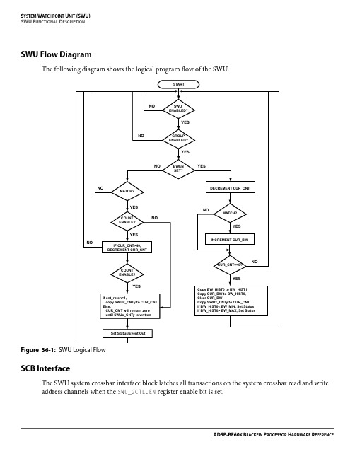
SYSTEM WATCHPOINT UNIT (SWU) SWU FUNCTIONAL DESCRIPTION
SWU Flow Diagram
The following diagram shows the logical program flow of the SWU.
67$57
12
6:8
(1$%/('"
- 1、下载文档前请自行甄别文档内容的完整性,平台不提供额外的编辑、内容补充、找答案等附加服务。
- 2、"仅部分预览"的文档,不可在线预览部分如存在完整性等问题,可反馈申请退款(可完整预览的文档不适用该条件!)。
- 3、如文档侵犯您的权益,请联系客服反馈,我们会尽快为您处理(人工客服工作时间:9:00-18:30)。
TO-220AB
Absolute Maximum Ratings
Parameter
VCES IC @ TC = 25°C IC @ TC = 100°C ICM ILM IF @ TC = 100°C IFM VGE PD @ TC = 25°C PD @ TC = 100°C TJ TSTG Collector-to-Emitter Voltage Continuous Collector Current Continuous Collector Current Pulsed Collector Current Clamped Inductive Load Current Diode Continuous Forward Current Diode Maximum Forward Current Gate-to-Emitter Voltage Maximum Power Dissipation Maximum Power Dissipation Operating Junction and Storage Temperature Range Soldering Temperature, for 10 sec. Mounting Torque, 6-32 or M3 Screw.
2
元器件交易网
IRG4BC30FD
20
16
Load Current ( A )
D uty cy cle: 50% TJ = 125°C T sink = 90° C G ate drive as s pecified Turn-on loss es inc lude effec ts of rev ers e rec overy
Min.
-------------------------
Typ.
----------0.50 ----2 (0.07)
Max.
1.2 2.5 -----80 ------
Units
°C/W
g (oz)
1
12/8/98
元器件交易网
IRG4BC30FD
Electrical Characteristics @ TJ = 25°C (unless otherwise specified)
Parameter Min. Collector-to-Emitter Breakdown Voltage 600 DV(BR)CES/DTJ Temperature Coeff. of Breakdown Voltage ---VCE(on) Collector-to-Emitter Saturation Voltage ---------VGE(th) Gate Threshold Voltage 3.0 DVGE(th)/DTJ Temperature Coeff. of Threshold Voltage ---gfe Forward Transconductance 6.1 ICES Zero Gate Voltage Collector Current ------V FM Diode Forward Voltage Drop ------IGES Gate-to-Emitter Leakage Current ---V(BR)CES Typ. ---0.69 1.59 1.99 1.70 ----11 10 ------1.4 1.3 ---Max. Units Conditions ---V VGE = 0V, IC = 250µA ---- V/°C VGE = 0V, IC = 1.0mA 1.8 IC = 17A VGE = 15V ---V IC = 31A See Fig. 2, 5 ---IC = 17A, TJ = 150°C 6.0 VCE = VGE, IC = 250µA ---- mV/°C VCE = VGE, IC = 250µA ---S VCE = 100V, IC = 17A 250 µA VGE = 0V, VCE = 600V 2500 VGE = 0V, VCE = 600V, TJ = 150°C 1.7 V IC = 12A See Fig. 13 1.6 IC = 12A, TJ = 150°C ±100 nA VGE = ±20V
1000
1000
I C , Collector-to-Emitter Current (A)
100
TJ = 25°C
I C , Colleቤተ መጻሕፍቲ ባይዱtor-to-Emitter Current (A)
100
T J = 150°C
TJ = 150°C T J = 25°C
10
10
1 1
V G E = 15V 20µs PULSE WIDTH A
Switching Characteristics @ TJ = 25°C (unless otherwise specified)
Qg Qge Qgc td(on) tr td(off) tf Eon Eoff Ets td(on) tr td(off) tf Ets LE Cies Coes Cres t rr Irr Qrr di(rec)M/dt Parameter Total Gate Charge (turn-on) Gate - Emitter Charge (turn-on) Gate - Collector Charge (turn-on) Turn-On Delay Time Rise Time Turn-Off Delay Time Fall Time Turn-On Switching Loss Turn-Off Switching Loss Total Switching Loss Turn-On Delay Time Rise Time Turn-Off Delay Time Fall Time Total Switching Loss Internal Emitter Inductance Input Capacitance Output Capacitance Reverse Transfer Capacitance Diode Reverse Recovery Time Diode Peak Reverse Recovery Current Diode Reverse Recovery Charge Diode Peak Rate of Fall of Recovery During tb Min. ---------------------------------------------------------------------------------Typ. 51 7.9 19 42 26 230 160 0.63 1.39 2.02 42 27 310 310 3.2 7.5 1100 74 14 42 80 3.5 5.6 80 220 180 120 Max. Units Conditions 77 IC = 17A 12 nC VCC = 400V See Fig. 8 28 VGE = 15V ---TJ = 25°C ---ns IC = 17A, VCC = 480V 350 VGE = 15V, RG = 23W 230 Energy losses include "tail" and ---diode reverse recovery. ---mJ See Fig. 9, 10, 11, 18 3.9 ---TJ = 150°C, See Fig. 9, 10, 11, 18 ---ns IC = 17A, VCC = 480V ---VGE = 15V, RG = 23W ---Energy losses include "tail" and ---mJ diode reverse recovery. ---nH Measured 5mm from package ---VGE = 0V ---pF VCC = 30V See Fig. 7 ---ƒ = 1.0MHz 60 ns TJ = 25°C See Fig. 120 TJ = 125°C 14 IF = 12A 6.0 A TJ = 25°C See Fig. 10 TJ = 125°C 15 VR = 200V 180 nC TJ = 25°C See Fig. 600 TJ = 125°C 16 di/dt 200A/µs ---- A/µs TJ = 25°C See Fig. ---TJ = 125°C 17
Power D iss ipa tion = 21W
12 6 0 % o f ra te d vo lt a g e 8
I
4
0 0.1 1 10
A
100
f, Frequency (kH z)
Fig. 1 - Typical Load Current vs. Frequency
(Load Current = IRMS of fundamental)
Max.
600 31 17 120 120 12 120 ± 20 100 42 -55 to +150 300 (0.063 in. (1.6mm) from case) 10 lbf•in (1.1 N•m)
Units
V
A
V W
°C
Thermal Resistance
Parameter
RqJC RqJC RqCS RqJA Wt Junction-to-Case - IGBT Junction-to-Case - Diode Case-to-Sink, flat, greased surface Junction-to-Ambient, typical socket mount Weight
元器件交易网
PD -91451B
IRG4BC30FD
INSULATED GATE BIPOLAR TRANSISTOR WITH ULTRAFAST SOFT RECOVERY DIODE