9701_s17_qp_52
RT9817 产品数据手册说明书

1DS9817-13 April 2022Features●Internally Fixed Threshold 1.2V to 5V in 0.1V Step ●High Accuracy ±1.5%●Low Supply Current 3μA●No External Components Required ●Quick Reset within 20μs●Built-in Recovery Delay Include 0ms, 55ms, 220ms,450ms Options●Low Functional Supply Voltage 0.9V ●CMOS Push-Pull Output●Small SC-82 and SOT-143 Packages●RoHS Compliant and 100% Lead (Pb)-FreePin ConfigurationApplications●Computers ●Controllers●Intelligent Instruments●Critical μP and μC Power Monitoring ●Portable/Battery-Powered EquipmentMicro-Power Voltage Detectors with Manual ResetOrdering InformationGeneral DescriptionThe RT9817 is a micro-power voltage detector with deglitched manual reset input supervising the power supply voltage level for microprocessors (μP) or digital systems. It provides internally fixed threshold levels with 0.1V per step ranging from 1.2V to 5V, which covers most digital applications. It features low supply current of 3μA.The RT9817 performs supervisory function by sending out a reset signal whenever the V DD voltage falls below a preset threshold level. This reset signal will last the whole period before V DD recovering. Once V DD recovered upcrossing the threshold level, the reset signal will be released after a certain delay time. To pull reset signal low manually, just pull the manual reset input (MR) below the specified V IL level. RT9817 is provided in SC-82 and SOT-143 packages.(TOP VIEW)SOT-143Marking Information For marking information, contact our sales representative directly or through a RichTek distributor located in your area, otherwise visit our website for detail.Note :Richtek p roducts are :❝RoHS compliant and compatible with the current require- ments of IPC/JEDEC J-STD-020.❝Suitable for use in SnPb or Pb-free soldering processes.SC-82RESET/RESET MRRESET/RESET MR RT9817A = 0ms (RESET)B = 55ms (RESET)C = 220ms (RESET)D = 450ms (RESET)E = 0ms (RESET)F = 55ms (RESET)G = 220ms (RESET)H = 450ms (RESET)2DS9817-13 April 2022 Functional Block DiagramTypical Application CircuitFunctional Pin DescriptionRESET/RESETMRPart StatusThe part status values are defined as below :Active : Device is in production and is recommended for new designs. Lifebuy : The device will be discontinued, and a lifetime -buy period is in effect. NRND : Not recommended for new designs.Preview : Device has been announced but is not in production. Obsolete : Richtek has discontinued the production of the device.3DS9817-13 April 2022Absolute Maximum Ratings (Note 1)●Terminal Voltage (with Respect to GND)V DD ------------------------------------------------------------------------------------------------------------------------−0.3V to 6.0V●All Other Inputs --------------------------------------------------------------------------------------------------------−0.3V to V DD +0.3V ●Input Current, I VDD -----------------------------------------------------------------------------------------------------20mA ●Power Dissipation, PD @ T A = 25°CSC-82--------------------------------------------------------------------------------------------------------------------0.25W SOT-143-----------------------------------------------------------------------------------------------------------------0.285W ●Package Thermal Resistance (Note 2)SC-82, θJA ---------------------------------------------------------------------------------------------------------------400°C SOT-143, θJA ------------------------------------------------------------------------------------------------------------350°C ●Lead Temperature (Soldering, 10sec.)---------------------------------------------------------------------------- 260°C●Storage T emperature Range ----------------------------------------------------------------------------------------−65°C to 125°C ●ESD Susceptibility (Note 3)HBM (Human Body Mode)------------------------------------------------------------------------------------------2kV MM (Machine Mode)--------------------------------------------------------------------------------------------------200VElectrical Characteristics(V= 3V, T = 25°C, unless otherwise specified)Recommended Operating Conditions (Note 4)●Junction T emperature Range ----------------------------------------------------------------------------------------−40°C to 125°C ●Ambient T emperature Range ----------------------------------------------------------------------------------------−40°C to 85°CTo be continued4DS9817-13 April 2022Note 1. Stresses listed as the above “Absolute Maximum Ratings ” may cause permanent damage to the device. These are forstress ratings. Functional operation of the device at these or any other conditions beyond those indicated in the operational sections of the specifications is not implied. Exposure to absolute maximum rating conditions for extended periods may remain possibility to affect device reliability.Note 2. θJA is measured in the natural convection at T A = 25°C on a low effective thermal conductivity test board ofJEDEC 51-3 thermal measurement standard.Note 3. Devices are ESD sensitive. Handling precautions are recommended.Note 4. The device is not guaranteed to function outside its operating conditions.5DS9817-13 April 2022Typical Operating CharacteristicsSupply Current vs. Input Voltage01234123456Input Voltage (V)S u p p l y C u r r e n t I D D (u A )Output Voltage vs. Input Voltage012345670123456Input Voltage (V)O u t p u t V o l t a g e (V)Nch Driver Output Current vs. V DS020*********120012345V DS (V)O u t p u t C u r r e n t(m A )Supply Current vs. Input Voltage01234560123456Input Voltage (V)S u p p l y C u r r e n t (u A )Nch Driver Output Current vs. V DS010********600.511.522.533.5V DS (V)O u t p u t C u r r e n t (m A )Nch Driver Output Current vs. V DS00.40.81.21.622.400.30.60.91.21.5V DS (V)O u t p u t C u r r e n t(m A )6DS9817-13 April 2022 Nch Driver Sink Current vs. Input Voltage0102030400.511.522.533.5Input Voltage (V)S i n k C u r r e n t I S I N K (m A )Supply Current vs. Input Voltage01234123456Input Voltage (V)S u p p l y C u r re n t (u A )Power-Down Reset Delay vs. Temperature051015202530354045-50-25255075100125Temperature P o w e r -D o w n R e s e t D e l a y (u s)(°C)Power-Down Reset Delay vs. Temperature051015202530354045-50-25255075100125Temperature P o w e r -D o w n R e s e t D e l a y (u s )(°C)Power-Down Reset Delay vs. Temperature03691215-50-25255075100125Temperature P o w e r -D o w n R e s e t D e l a y (u s )(°C)Nch Driver Sink Current vs. Input Voltage0102030405012345Input Voltage (V)S i n k C u r r e n t I S I N K (m A )7DS9817-13 April 2022Output Delay Time vs. Load Capacitance0.010.111010010000.00010.00100.01000.1000 1.0000Load Capacitance (uF)O u t p u t D e l a y T i m e (m s )Power-Up Reset Time-Out vs. Temperature0255075100-50-25255075100125Temperature P o w e r -U p R e s e t T im e -O u t (m s )(°C)Reset Threshold Deviation vs. Temperature1.002.003.004.005.006.00-50-25255075100125Temperature R e s e t T h r e s h o l d D e v i a t i on (V )(°C)Pch Driver Output Current vs. Input Voltage0510152025123456Input Voltage (V)O u t p u t C u r r e n t(m A )Nch Driver Output Current vs. V DS204060801001201401600123456V DS (V)N c h D r i v e r O u t p u t C ur r e n t (m A )Power-Up Reset Time-Out vs. Temperature0100200300400500-50-25255075100125Temperature P o w e r -U p R e s e t T i me -O u t (m s )(°C)8DS9817-13 April 2022 Nch Driver Output Current vs. Input Voltage1020304050600123456Input Voltage (V)N c h D r i v e r O u t p u t C u r r e n t (m A )Output Voltage vs. Input Voltage01234567123456Input Voltage (V)O u t p u tV o l t a g e (V )Power-Down Reset Time-Out vs. Temperature051015202530-50-25255075100125Temperature P ow e r -D o w n R e s e t T i m e -O u t (u s )(°C)Power Down Reset Time-Out vs. Temperature0100200300400500-50-25255075100125Temperature P o w e r D o w n R e s e t T i m e -O u t (m s )(°C)9DS9817-13 April 2022Application InformationBenefits of Highly Accurate Reset ThresholdMost μP supervisor ICs have reset threshold voltages between 1% and 1.5% below the value of nominal supply voltages.This ensures a reset will not occur within 1% of the nominal supply, but will occur when the supply is 1.5% below nom inal.10DS9817-13 April 2022SOT-143 Surface Mount Package11DS9817-13 April Richtek Technology CorporationHeadquarter5F, No. 20, Taiyuen Street, Chupei CityHsinchu, Taiwan, R.O.C.Tel: (8863)5526789 Fax: (8863)5526611Information that is provided by Richtek Technology Corporation is believed to be accurate and reliable. Richtek reserves the right to make any change in circuit design,specification or other related things if necessary without notice at any time. No third party intellectual property infringement of the applications should be guaranteed by users when integrating Richtek products into any application. No legal responsibility for any said applications is assumed by Richtek.Richtek Technology Corporation Taipei Office (Marketing)5F, No. 95, Minchiuan Road, Hsintien City Taipei County, Taiwan, R.O.C.Tel: (8862)86672399 Fax: (8862)86672377Email:*********************SC -82 Surface Mount Package。
RT9705B 1 DS9705B-03 电源多路复用器说明书

DS9705B-03 April 201180m Ω, 1A Power MultiplexerGeneral DescriptionThe RT9705B is a dual input single output power multiplexer specifically designed to provide seamless voltage transition between two independent power suppliers. Equipped with two low R DS(ON) N-Channel MOSFETs driven by internal charge pump circuitry, the RT9705B is able to deliver 1A output current with only 80mV voltage drop. Manual or auto switching mode is easily selected by two digital inputs D1 and D0. When both D0and D1 are selected high, the RT9705B enters shutdown mode and consumes minimum power making it ideal suitable for battery powered equipments. A STAT pin with open drain output is provided to indicate the switch status.A user-programmable up to 1.25A current limit function is available for maximum safety in various applications.The RT9705B provides comprehensive protection functions,including adjustable current limit, over temperature protection, soft start function for minimum inrush current,cross-conduction protection, and reverse conduction protection. These features greatly simplify power multiplexer design. The RT9705B is available in TSSOP-8package requiring minimum board area and smallest components.Featuresz Adjustable Current Limiting up to 1.25Az Built-In (Typically 80m Ω) N-Channel MOSFET zReverse Current Flow Blocking (no body diode) i.e.Output Can Be Forced Higher than Input (Off-State)zLow Supply Current :`55μA Typical at Switch on State`Less than 0.5μA Typical at Switch Off State z Guaranteed 1A Continuous Load Current z Wide Input Voltage Ranges : 2.8V to 5.5V z Open-Drain STAT Outputz Hot Plug-In Application (Soft-Start)z Thermal Shutdown Protectionz Smallest TSSOP-8 Package Minimizes Board Space zRoHS Compliant and 100% Lead (Pb)-FreeApplicationsz LCD Monitor, LCD-TVz Information Appliance and Set-Top Box z Battery-Powered Equipment z ACPI Power Distributionz Motherboard & Notebook PCs z Mini PCI & PCI-Express Cards zPCMCIA & New CardsPin Configurations(TOP VIEW)TSSOP-8Ordering InformationSTAT D0D1ILIMGNDVIN2VOUT VIN1Note :Richtek products are :` RoHS compliant and compatible with the current require-ments of IPC/JEDEC J-STD-020.` Suitable for use in SnPb or Pb-free soldering processes.Marking InformationFor marking information, contact our sales representative directly or through a Richtek distributor located in yourarea.Package Type C : TSSOP-8RT9705BLead Plating System P : Pb FreeG : Green (Halogen Free and Pb Free)Typical Application CircuitTable 1. Truth TableNotes for Table 1.1. X : Don ’t care2. Hi-Z: High impedance node3. D0 and D1 cannot be floating which will lead to an unknown state.4. An internal MOSFET with 2k Ω R DS(ON) turns on and softly discharges the output voltage when D0 = D1 = 1.V V OUTDS9705B-03 April 2011Test CircuitsTest Circuit 1Test Circuit 2Test Circuit 3Test Circuit 4f = 28Hzf = 580Hz5VV OUTFunction Block DiagramTiming DiagramV 5VQ1 EnabledQ2 EnabledV 3.3VV OUT (a)(b)(c)DS9705B-03 April 2011Electrical Characteristicsz Input Voltage, VIN1 & VIN2-----------------------------------------------------------------------------------------−0.3V to 6.0V z Logic Inputs Voltage, D0 &D1--------------------------------------------------------------------------------------−0.3V to 6.0V z Output Voltage, VOUT , STAT & ILIM -----------------------------------------------------------------------------−0.3V to 6.0V zPower Dissipation, P D @ T A = 25°CTSSOP-8----------------------------------------------------------------------------------------------------------------0.43W zPackage Thermal Resistance (Note 2)TSSOP-8, θJA ----------------------------------------------------------------------------------------------------------230°C/W z Junction T emperature -------------------------------------------------------------------------------------------------125°C z Lead Temperature (Soldering, 10 sec.)---------------------------------------------------------------------------260°Cz Storage T emperature Range ----------------------------------------------------------------------------------------−65°C to 150°C zESD Susceptibility (Note 3)HBM (Human Body Mode)------------------------------------------------------------------------------------------2kV MM (Machine Mode)--------------------------------------------------------------------------------------------------200VAbsolute Maximum Ratings (Note 1)To be continuedRecommended Operating Conditions (Note 4)zInput VoltageV IN1 ( if V IN2 2.8V)--------------------------------------------------------------------------------------------------2.3V to 5.5V V IN1 ( if V IN2 < 2.8V)--------------------------------------------------------------------------------------------------2.8V to 5.5V V IN2 ( if V IN1 2.8V)--------------------------------------------------------------------------------------------------2.3V to 5.5V V IN2 ( if V IN1 < 2.8V)--------------------------------------------------------------------------------------------------2.8V to 5.5V z Logic Inputs Voltage (D0 &D1)-------------------------------------------------------------------------------------0V to 5.5V z Junction T emperature Range ----------------------------------------------------------------------------------------−40°C to 125°C z Ambient T emperature Range ----------------------------------------------------------------------------------------−40°C to 85°C≥≥To be continuedDS9705B-03 April 2011Note 1. Stresses listed as the above “Absolute MaximumRatings ” may cause permanent damage to the device. These are for stress ratings. Functional operation of the device at these or any other conditions beyond those indicated in the operational sections of the specifications is not implied.Exposure to absolute maximum rating conditions for extended periods may remain possibility to affect device reliability.Note 2. θJA is measured in the natural convection atT A = 25°C on a low effective thermal conductivity test board of JEDEC 51-3 thermal measurement standard.Note 3. Devices are ESD sensitive. Handling precautionrecommended.Note 4. The device is not guaranteed to function outside itsoperating conditions.Note 5. Performance at −5°C ≤ T A ≤ 85°C is assured bydesign.Note 6. Not tested for production.Note 7. The UVLO is without latch. In V IN falling dege, theoutput voltage will depend on I OUT and C OUT . Please see below curve as reference.V IN2 = 2.2V, C OUT = 10uF, R L = 180ΩV OUT Response vs. UVLOTime (1ms/Div)V OUT(1V/Div)V IN1(1V/Div)R DS(ON) vs. Temperature5060708090100110-50-25255075100125Temperature (°C)R D S (O N ) (m Ω)Typical Operating CharacteristicsR e f e r t o T e s t C i r c u i t s 2Output Turn-On ResponseTime (1ms/Div)D0D1V OUT(2V/Div)(2V/Div)(2V/Div)D0 = 1 0, D1 = 1, V IN1 = 5V, V IN2 = 3.3V↔Output Switchover ResponseTime (1ms/Div)D1D0V OUT(2V/Div)(2V/Div)(2V/Div)D0 = 0, D1 = 1 0V IN1 = 5V, V IN2 = 3.3V↔R e f e r t o T e s t C i r c u i t s 1Current Limit vs. Junction Temperature00.20.40.60.811.21.41.61.82-50-25255075100125Junction Temperature C u rr e n t L i m i t (A )(°C)R DS(ON) vs. Input Voltage606570758085902.53 3.54 4.55 5.56Input Voltage (V)R D S (O N ) (m Ω)Quiescent Current vs. Input Voltage303540455055602.53 3.54 4.55 5.56Input Voltage (V)Q u i e s c e n t C u r r en t (u A )DS9705B-03 April 2011Output Switchover Voltage DroopTime (50μs/Div)D1V OUT(2V/Div)(2V/Div), C OUT = 1uF (2V/Div), C OUT = openD0 = 0, D1 = 1 0, V IN1 = V IN2 = 5V, RL = 50Ω↔R e f e r t o T e s t C i r c u i t s 3Auto Switchover Voltage DroopTime (250μs/Div)(2V/Div)(2V/Div)V OUTV IN1D0 = 1, D1 = 0, V IN1 = 5 0V, V IN2 = 3.3V↔R e f e r t o T e s t C i r c u i t s 4Output Switchover Voltage Droop vs. C OUT00.20.40.60.811.21.41.60.1110100C OUT (uF)O u t p u t S w i t c h o v e r V o l t a g e D r o o p (V )Application InformationThe RT9705B is dual input single output power multiplexer specifically designed to provide seamless voltage transition between two independent power suppliers. Equipped with two low R DS(ON) N-Channel MOSFETs driven by internal charge pump circuitry, the RT9705B is able to deliver 1A output current with only 80mV voltage drop. The RT9705B provides comprehensive protection functions, including adjustable current limit, over temperature protection, soft start function for minimum inrush current, cross-conduction protection, and reverse conduction protection. These features greatly simplify power multiplexer design.Manual Switching ModeThe RT9705B provides two logic input D0 and D1 for switch selection as shown in Table 1. The RT9705B selects the manual-switching mode when the D0 is pulled low. In this mode V OUT connects to V IN1 if D1 pulled high, otherwise V OUT connects to V IN2.Auto Switching ModeRT9705B selects the auto-switching mode when the D0 is pulled high and D1 is pulled low. In this mode V OUT connects to the higher of V IN1 and V IN2.Shutdown ModeWhen both D0 and D1 are selected high, the RT9705B enters shutdown mode and consumes minimum power. An internal MOSFET with 2kΩ R DS(ON) turns on and softly discharges the output voltage in the shutdown mode. Since no body diode exists between V INX and V OUT, output voltage is allowed to be high than the input voltages in the shutdown mode.Switch Status IndicationA STAT pin with open drain output is provided to indicate the switch status. STAT pin outputs high impedance if V IN2 is active, otherwise STAT pin outputs low.Current LimitingThe current limit circuitry prevents damage to the MOSFET switch and external load. A resistor R ILIM from ILIM to GND sets the current limit to 500/R ILIM and the adjustable current limiting up to 1.25 A. A setting resistor R ILIM equal to zero is not recommended as that disables current limiting.Thermal ConsiderationsThermal protection limits power dissipation in RT9705B. When the operation junction temperature exceeds 135°C, the OTP circuit starts the thermal shutdown function and turns the pass element off. The pass element turn on again after the junction temperature cools by 10°C.For continuous operation, do not exceed absolute maximum operation junction temperature 125°C. The power dissipation definition in device is :P D = (V IN-V OUT) x I OUT + V IN x I QThe maximum power dissipation depends on the thermal resistance of IC package, PCB layout, the rate of surroundings airflow and temperature difference between junction to ambient. The maximum power dissipation can be calculated by following formula :P D(MAX) = ( T J(MAX) - T A ) / θJAwhere T J(MAX) is the maximum operation junction temperature 125°C, T A is the ambient temperature and the θJA is the junction to ambient thermal resistance.For recommended operating conditions specification of RT9705B, where T J(MAX) is the maximum junction temperature of the die (125°C) and T A is the maximum ambient temperature. The junction to ambient thermal resistance (θJA is layout dependent) for TSSOP-8 package is 230°C/W on standard JEDEC 51-3 thermal test board. The maximum power dissipation at T A = 25°C can be calculated by following formula :P D(MAX) = (125°C -25°C) / 230°C/W = 430 mW (TSSOP-8)RT9705B11DS9705B-03 April 2011Layout ConsiderationIn order to meet the voltage drop, droop, and EMI requirements, careful PCB layout is necessary. The following guidelines must be considered :zKeep all main current traces as short and wide as possible.z Place a ground plane under all circuitry to lower both resistance and inductance and improve DC and transient performance (Use a separate ground and power plans if possible).zLocate the ceramic input capacitors as close as possible to the VIN and GND pins of the device.Figure 1. Top Layer Figure 2. Bottom Layer12DS9705B-03 April Richtek Technology CorporationHeadquarter5F, No. 20, Taiyuen Street, Chupei CityHsinchu, Taiwan, R.O.C.Tel: (8863)5526789 Fax: (8863)5526611Richtek Technology Corporation Taipei Office (Marketing)5F, No. 95, Minchiuan Road, Hsintien City Taipei County, Taiwan, R.O.C.Tel: (8862)86672399 Fax: (8862)86672377Email:*********************Information that is provided by Richtek Technology Corporation is believed to be accurate and reliable. Richtek reserves the right to make any change in circuit design,specification or other related things if necessary without notice at any time. No third party intellectual property infringement of the applications should be guaranteed by users when integrating Richtek products into any application. No legal responsibility for any said applications is assumed by Richtek.8-Lead TSSOP Plastic Package。
U盘主控芯片IS917

3. Pin Assignmestor Technology Corporation
5
12 VCC18O 11 DAT[0] 10 DAT[1] 9 DAT[2] 8 DAT[3] 7 DVDD12 6 DQS 5 VCCQ 4 DAT[4] 3 DAT[5] 2 DAT[6] 1 DAT[7]
Innostor Technology Corporation
2
Innostor Technology Corporation
IS917 USB3.0 Flash Disk Controller
Table of Contents :
1. DESCRIPTION ........................................................................................................ 4 2. FEATURES ............................................................................................................. 4 3. PIN ASSIGNMENT .................................................................................................. 5
Innostor Technology Corporation
IS917 USB3.0 Flash Disk Controller
3.2 Pin Descriptions
中兴交换机配置

一、系统的启动过程如下。
1、上电后,首先进行硬件启动,当硬件检测无误后,管理终端上出现下列信息:Welcome to use ZTE eCarrier!!Copyright(c) 2004-2006, ZTE Co。
, Ltd.System Booting..。
.。
CPU: S3C45010 ARM7TDMIBSP version: 1.2/0Creation date: Feb 11 2004, 09:37:01Press any key to stop auto-boot。
..72、出现上述信息后,等待大约7 秒,用户可以在这段时间内按任意键进入boot 状态,修改启动参数.当系统在规定时间未检测到用户输入时,系统便开始自动加载版本,并提示下列信息:auto—booting。
..boot device : secEndunit number : 0processor number : 0host name : tigerfile name : vxWorksinet on ethernet (e) : 10.40.92。
106host inet (h) : 10。
40.92.105flags (f) : 0x80Attaching to TFFS.。
done。
Loading version:/kernel.。
.1459932 + 75292 + 6358852Starting at 0x1656e0...Attaching interface lo0。
.。
done(省略)Welcome !ZTE Corporation。
All rights reserved.login:adminpassword:*********3、系统启动成功后,出现提示符login:,要求输入登录用户名和密码,缺省用户名是admin,密码是zhongxing。
二、配置开始工作1.打开超级终端,输入连接的名称,如ZXR10,并选择一个图标。
ICDPPCNEXUS MPC55xx MPC56xx In-Circuit Debugger

ICDPPCNEXUSMPC55xx / MPC56xx In-Circuit DebuggerQuick Start GuideCopyright 2009, P&E Microcomputer Systems, Inc. All rights reserved.Visit us on the web at Document Version HistoryVersion Date Notes1.0 21 Sep 2009 Initial versionCONTENTS1 Introduction (4)1.1 P&E Compatible Hardware (4)2 Getting Started (5)2.1 Connecting to your Target (5)2.2 Reset Script (6)2.3 Loading Data and Debug Information (7)2.4 CPU and Memory Windows (8)3 Debugging (10)3.1 GOTIL command (10)3.1 Stepping through C instructions (11)3.3 Setting and Reaching Breakpoints (12)3.4 Using Code Window Popup Debug Evaluation Hints (13)3.5 Using the Variables Window (15)3.6 Modifying a Variable (16)3.7 Using the Register Interpreter (17)3.8 Adding Register Field Descriptions to the Variables Window (20)1 IntroductionThis document is a step-by-step guide to using the P&E ICDPPCNEXUS in-circuit debugger software, which is compatible with Freescale MPC55xx / MPC56xx processors. This guide covers the most commonly used features of the debugger: loading binary & debug information, accessing CPU registers & memory, stepping code, setting breakpoints, and monitoring variables.1.1 P&E Compatible HardwareThe following lists the P&E hardware compatible with the ICDPPCNEXUS debugger software.P&E Part Number Interface to host PCCABPPCNEXUS Parallel (LPT) portUSB-ML-PPCNEXUS USB 2.0 (Backwards compatible with USB 1.1 ports) Cyclone MAX Serial (RS232) portUSB 1.1 (Upwards compatible with USB 2.0 ports)Ethernet2 Getting Started2.1 Connecting to your TargetUpon starting the debugger, the connection assistant dialog appears:•Use the “Interface” and “Port” drop-down menus to choose the P&E hardware interface connected between the PC and your target board.•The “Target CPU” setting can safely be left at the “Autodetect” setting for most users. If you experience problems connecting, you can try specifying the exact Freescale device that you are connecting to.• A BDM_SPEED parameter between 2 to 4 can typically be used.Processors running at slower clock speeds will require higher values.Click the Connect button, and ICDPPCNEXUS will attempt to contact the processor. Using the default debugger settings, ICDPPCNEXUS will establish communications and reset the processor.After establishing communications, the main debugger screen will appear, and a debugger reset script macro should automatically execute and complete.2.2 Reset ScriptThis section explains the initialization that the debugger, using a reset script macro file, performs on the processor. The user can view and modify all of the macro file's initialization tasks.The processor Boot Assist Module (BAM) would normally initialize the memory of the processor. However, when running the target application from the debugger, the BAM functionality is disabled. To account for this, the debugger must run a script file on reset. The script initializes the memory of the processor similar to the way in which the BAM would initialize the processor.If ICDPPCNEXUS is launched from the Freescale CodeWarrior IDE, the correct reset script file is automatically selected.If ICDPPCNEXUS is launched stand-alone, the reset script file may need to be configured. Several reset script macros are included with the ICDPPCNEXUS debugger and have a .mac extension. For detailed information, you can view each macro file using a simple text editor such as Notepad. The macro contents will contain useful comments, such as which devices are supported by that particular macro.To configure the debugger reset script macro, select the debugger Configuration menu, Automated Script Options dialog, shown here:2.3 Loading Data and Debug InformationIf ICDPPCNEXUS is launched from the Freescale CodeWarrior IDE, your code will automatically be downloaded to the processor.•RAM projects are loaded into the processor’s internal SRAM.•FLASH projects will invoke the CPROGPPCNEXUS Flash programming software to burn the code into the processor’s internal FLASH.The debug information is also automatically loaded from CodeWarrior, which will allow you to debug using your high level source code and variables.If ICDPPCNEXUS is launched stand-alone, you will need to manually download the code and debug information. Launch the Load Dialog by clicking on the High Level Load button on the debugger tool bar:This dialog allows you to specify the binary/debug file and whether to load into RAM or FLASH. Once you are satisfied with your settings, press the “Process Load Command” button to begin the download process. This step will also load the debug information.2.4 CPU and Memory WindowsThe CPU Window displays all CPU core registers, including the Program Counter (PC) and all general purpose registers.•To modify CPU register contents, double-click the register value. You will be prompted for a new value.The Memory Window displays data at any given memory address. It can be used to view RAM contents, FLASH contents, and values of peripheral registers.•To change the memory address, right-click inside the Memory Window and select “Set Base Address”. You will be prompted for a new address to begin displaying data.•To change the contents in memory, double-click the value in memory that you would like to change. You will be prompted for a new value.3 DebuggingThis section outlines the different debugging capabilities available in the ICDPPCNEXUS debugger once the debug information has been loaded.3.1 GOTIL commandAt this point, your source window will show the assembly language startup code generated by the compiler:If you do not need to debug this section and would like to run the processor until the beginning of your “main” function, you can use the “GOTIL” command.•Type “GOTIL main” in the Status window to tell the debugger to run code until it reaches the “main” function of your code.The “GOTIL” command works with any function in your code.3.1 Stepping through C instructionsStep through the initialization code, or any source code, using the high-level language source step command. Use this feature by typing “HSTEP” in the Status window or by clicking the high-level step button on the debugger tool bar:Each time the HSTEP command executes, the debugger will rapidly single step assembly instructions until it encounters the next source instruction, at which point target execution will cease. When the debugger reaches the next source instruction, all visible windows will be updated with data from the board. After reaching the main function, step through several C language instructions. Notice that some instructions will take longer to step through than others because each C instruction may consist of a greater or fewer number of underlying assembly instructions.3.3 Setting and Reaching BreakpointsIn the source code window, there will be a small red dot and a small blue arrow next to each source instruction that has underlying object code. If a large blue arrow appears on a source line, this indicates that the program counter (PC) currently points to this instruction. If a large red stop sign appears on the source line, this indicates that a breakpoint exists on this line.•Set a breakpoint at an instruction by double-clicking the tiny red dot.•To remove a breakpoint, double-click the large red stop sign.Execution will begin in real-time when you issue the HGO command or click the high-level language GO button on the debugger tool bar:If the debugger encounters a breakpoint, execution will stop on this source line. If it does not encounter a breakpoint, target execution will continue until you press a key or use the stop button on the debugger tool bar:•By double clicking the small blue arrow, you will be issuing a GOTIL command to the address of this source line.A GOTIL command will set a single breakpoint at the desired address, and the processor will begin executing code in real-time from the current program counter (PC). When the debugger encounters the GOTIL address, execution stops. If the debugger does not encounter this location, execution continues until you press akey or use the stop button on the debugger tool bar. Note that all user breakpoints are ignored when the GOTIL command is used.You may also double-click the red and blue symbols in the disassembly window. The disassembly window may display an additional symbol, a small, blue "S" enclosed in a box. This indicates that that a source code instruction begins on this disassembly instruction.3.4 Using Code Window Popup Debug Evaluation HintsWhen debugging source code, it is convenient to view the contents of a variable while viewing your source code. The in-circuit debugger has a feature, debug hints, which displays the value of a variable while the mouse cursor is held over the variable name. The hint may be displayed in any of three locations, as shown below.The three locations for the debug hints are the code window title bar, the status window caption bar, and a popup hint that appears over the variable in source code. You can configure the hints to display in any combination.•Set the locations of debug hints in the configuration menu of the debuggerThe information in the popup hint box is similar to the information displayed in the variables window.The information includes the variable name (i), value ($1), and type (signed long).3.5 Using the Variables WindowThe variables window displays the current value of application variables. The following window shows a display of variables from the example application.Variables that are pointer or reference types are displayed in red. Normal variables are displayed in black.•Add a variable by typing the VAR command, by right clicking the variables window and choosing “Add a variable”, or by hitting the "Add Variable"button in the variables window.When adding a variable using the pop-up menu, the debugger displays the following screen.In the variable field, type the address or name of the variable. Typically, set the type of the variable to “Default”, which means that the variable will be displayed as it is defined in the debugging information. When adding a variable, you may specify the numeric display base of the variable.3.6 Modifying a Variable•To modify the current value of a variable, right-click the variable name in the variables window and select “Modify Variable” to display a dialog.Check the “Modify value” checkbox, and type the variable’s new value. After you click the OK button, the debugger updates the variable value on the target, and the debugger refreshes the variable window to display the new value. Note that the debugger will not edit certain user-defined types, such as enumerated types.•You may also modify a variable’s display properties, such as the type or numeric display base using this dialog.3.7 Using the Register InterpreterThe register interpreter provides a descriptive display of bit fields within the processor’s peripheral registers. The register interpreter allows you easily to change the value of these registers. You may quickly check the current state of a peripheral and examine the configuration of the target device.When you use the register interpreter within the debugger, it reads the current value of the peripheral register, decodes it, and displays it.To launch the register interpreter in the debugger, either use the “R” command or click the view/edit register button on the tool bar:A window will appear that allows you to select a peripheral block to examine.Double clicking the module of choice will launch the register selection window.Double clicking a specific register will launch the edit/display window for that register.The window lists the keystrokes and mouse actions, allowing you to modify the values of each of the fields. After right clicking on a specific field, the register interpreter will display all options for that field.When you quit the register view/edit window by hitting the ESC key, you will be given the opportunity to write the new value into the register, as shown in the following window.3.8 Adding Register Field Descriptions to the Variables WindowAdd register bit fields to the variables window by using the “_TR” command in the debugger or by clicking the "Add Register" button in the variables window. After selecting the register field, the field appears in the debugger variables window, and the debugger will continually update its value.。
液晶显示器易损芯片故障列表

液晶显示器易损芯片故障列表AA T1101A M150XN05 屏电源管理芯片,损坏后表现为白屏‘开机图像暗淡等AAT1164 M170EG01 新款屏通病,主要用在明基FP71G+液晶显示器上面。
用一段时间会白屏、关机在开用一段时间又出现白.本芯片为液晶屏高压产生及管理芯片、明基液晶显示器常坏、故障为:白屏。
AA T1343 LG、PHILIPS 屏用,开机白屏、花屏、竖条等AD8567 友达屏用,白AU30707 友达屏用,白屏、花屏、图像淡AU30803 友达屏用,白屏、花屏、图像淡AUO-003 M170EG01 屏,主供电短路、开机白屏或画屏、开机彩色失真、彩色竖条等DS90C385 LVDS 发送器芯片FPD87326 LG PHILIPS ICGVS690H9 液晶ICHX8912TA 液晶ICLPD91821 三星液晶屏专用LRE031212A LTM170EU-L21 的屏主芯片LRU4312X1A 三星多款17 寸屏主芯片,损坏率高LXD91810LXD91811 三星14,15 寸屏主芯片,白屏、花屏、灰色竖条、无显示,可代替91812,91810LXD91812LXD91814LXD91820MST8116B CMV 和BENQ 等、液晶主芯片,此IC 损坏率高,出现故障:花屏、白屏、连接信号线无显示等MST8131A MST8131A MST8111B MST8111A 此四个型号通用,联想\宏基\BENQ 等液晶显示器主芯片,此IC 损坏率高,出现故障:花、白屏、连接信号线无显示等NT68521 4 合1 电视板芯片RTD2023 LVDS 图像信号处理芯片,M170EP01-2.0 版一体屏和多个厂家驱动板使用。
SE7889-LF 三星液晶显示器驱动板图像信号处理芯片,此IC 损坏率高,出现故障:花SN0209033PZP LG.Philips 液晶屏专用LM170E01TFP7425P 京东方现代屏时序控制器芯片,损坏率高TFP7433 京东方现代屏时序控制器芯片,损坏率高TSU16AK 图像信号处理芯片单片机NT68F63 三星,冠捷等液晶MCUNT68F633 PHILIPSWT61P4 三星液晶MCUW78E65 冠捷常用,可代替M6759,SM5964MTV312MTV512 BENQ,长城液晶常用。
IBM Storwize V7000 硬盘微码对照表
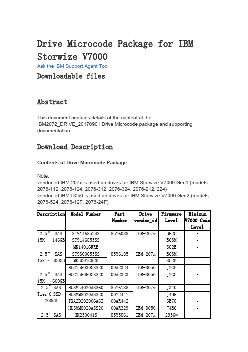
Drive Microcode Package for IBM Storwize V7000Ask the IBM Support Agent ToolDownloadable filesAbstractThis document contains details of the content of theIBM2072_DRIVE_20170901 Drive Microcode package and supporting documentation.Download DescriptionContents of Drive Microcode PackageNote:vendor_id IBM-207x is used on drives for IBM Storwize V7000 Gen1 (models 2076-112, 2076-124, 2076-312, 2076-324, 2076-212, 224)vendor_id IBM-D050 is used on drives for IBM Storwize V7000 Gen2 (models 2076-524, 2076-12F, 2076-24F)Level85Y5862v7.4.0.1 v6.3.0.04K BS** It is strongly recommended that customers with these drive model numbers (HUC106030CSS60, HUC106045CSS60, HUC106060CSS60) in their configuration, upgrade to this latest level of drive firmware.* If upgrading from 291E, please first upgrade to 2920 and then 2936. Please note: Ralston Peak 300 GB product_id=HUSML4030ASS60 is immune from this problem.2920 can be found on Fix Central in thispackage: StorageDisk-2076-DriveMicrocode-20121210Important Information:Drive Firmware upgrades are not supported on SAN Volume Controller or Storwize V7000 systems running V6.1 or V6.2. Please refer to the following Flash for more information.Drive Firmware Upgrades May Result in Temporary Loss of Host Access to Volumes on SAN Volume Controller and Storwize V7000Please refer to the svctask applydrivesoftware CLI command help in the IBM Storwize V7000 Information Center for installation instructions regarding this Drive Microcode Package.To check that your drive firmware is up to date download and run the Software Upgrade Test UtilityKeep Informed of UpdatesKeep up to date with the latest V7000 information by subscribing toreceive support notifications.Legal AgreementTHE FOLLOWING DOWNLOADS CONTAIN UPDATES AND FIXES TO CODE THAT WAS ORIGINALLY PROVIDED WITH THE IBM STORWIZEV7000 SOLUTION, INCLUDING THE IBM STORWIZE V7000 SOFTWARE. THE UPDATED CODE IS SUBJECT TO THE TERMS AND CONDITIONS OF THE LICENSE AGREEMENTS APPLICABLE TO THE CODE THAT IT UPDATES INCLUDING, AS APPROPRIATE, THE IBM AGREEMENT FOR MACHINE CODE AND IBM INTERNATIONAL PROGRAM LICENSE AGREEMENT. BY DOWNLOADING THE FOLLOWING FILES, YOU ARE AGREEING TO TREAT THE UPDATED CODE IN ACCORDANCE WITH THE APPLICABLE LICENSE AGREEMENTS.Download packageDESCRIPTION DOCUMENTATION LABEL DownloadOptionsPlatform IBMStorwize V7000Version IndependentEnglishByte Size 96217827Date 02 Sep 2017DriveMicrocodePackageHTTP。
QLogic QLE7340单口40GbpsQDR InfiniBand PCIe 2.0 X8主机

QLogic QLE7340 Single-Port 40 Gbps QDR InfiniBand Host Channel AdapterProduct Guide (withdrawn product)High-performance computing (HPC) solutions have used InfiniBand networks to meet the needs of the most demanding sets of applications and grand challenges. The QLE7340 is a single-port 40 Gbps InfiniBand PCI Express Gen2 x8 host channel adapter (HCA). It is a highly integrated design that delivers a high message rate and low latency, making it the ideal solution for HPC applications.Figure 1 shows the QLogic QLE7340 single-port 4X QDR IB PCIe 2.0 X8 host channel adapter.Figure 1. QLogic QLE7340 Single-Port 40 Gbps QDR InfiniBand HCADid you know?Click here to check for updatesDid you know?The QLogic QLE7340 HCA is part of IBM Intelligent Cluster solution (formerly IBM Systems Cluster 1350). IBM Intelligent Cluster is your key to a fully integrated HPC solution. IBM clustering solutions include servers, storage, and industry-leading OEM interconnects that are factory-integrated, fully tested, and delivered to your door, ready to plug into your data center, all with a single point of contact for support.Part number informationTable 1. Ordering part numbers and feature codesDescription Part number Feature code QLogic QLE7340 Single-Port 40 Gbps QDR InfiniBand HCA59Y188857630.5 m QLogic Copper QDR InfiniBand QSFP 30AWG Cable59Y189237251 m QLogic Copper QDR InfiniBand QSFP 30AWG Cable59Y189637263 m QLogic Copper QDR InfiniBand QSFP 28AWG Cable59Y190037273 m QLogic Optical QDR InfiniBand QSFP Cable59Y1920373110 m QLogic Optical QDR InfiniBand QSFP Cable59Y1924373230 m QLogic Optical QDR InfiniBand QSFP Cable59Y192837333m IBM Optical QDR InfiniBand QSFP Cable49Y0488598910m IBM Optical QDR InfiniBand QSFP Cable49Y0491599030m IBM Optical QDR InfiniBand QSFP Cable49Y04945991 Features and benefitsSupported serversThe QLogic QLE7340 HCA is supported in the IBM System x servers listed in Table 2 as part of the IBM Intelligent Cluster portfolio.Table 2. Supported servers in the IBM Intelligent Cluster portfolioQLogic QLE7340 HCA5763Y Y Y Y Y Y Y Y N N N N N Popular configurationsPopular configurationsFigure 2 illustrates how the QLogic QLE7340 HCA can be used in configurations. In this example, weconnect all InfiniBand HCAs to a QLogic 12200 QDR InfiniBand switch.Figure 2. x3650 M2 server with the QLogic QLE7340 HCA connected to an InfiniBand networkThe parts used are listed in Table 3.Table 3. Components used when connecting QLogic QLE7340 HCA to an InfiniBand network (Figure 2)Diagram reference Partnumber/machinetypeDescriptionQuantity Varies x3650 M2 or other supported server (See Table 2.)1 59Y1888QLogic QLE7340 HCA1 Varies QLogic QDR InfiniBand QSFP Cable, copper or optical (SeeTable 1.)1 0449-020QLogic 12200 (iDPx) 36-port QDR InfiniBand Switch Bundle1Supported operating systemsTrademarksLenovo and the Lenovo logo are trademarks or registered trademarks of Lenovo in the United States, other countries, or both. A current list of Lenovo trademarks is available on the Web athttps:///us/en/legal/copytrade/.The following terms are trademarks of Lenovo in the United States, other countries, or both:Lenovo®Intelligent ClusterSystem x®The following terms are trademarks of other companies:Linux® is the trademark of Linus Torvalds in the U.S. and other countries.Other company, product, or service names may be trademarks or service marks of others.。
- 1、下载文档前请自行甄别文档内容的完整性,平台不提供额外的编辑、内容补充、找答案等附加服务。
- 2、"仅部分预览"的文档,不可在线预览部分如存在完整性等问题,可反馈申请退款(可完整预览的文档不适用该条件!)。
- 3、如文档侵犯您的权益,请联系客服反馈,我们会尽快为您处理(人工客服工作时间:9:00-18:30)。
READ THESE INSTRUCTIONS FIRSTWrite your Centre number, candidate number and name on all the work you hand in.Write in dark blue or black pen.You may use an HB pencil for any diagrams or graphs.Do not use staples, paper clips, glue or correction fluid.DO NOT WRITE IN ANY BARCODES.Answer all questions.Electronic calculators may be used.You may lose marks if you do not show your working or if you do not use appropriate e of a Data Booklet is unnecessary.At the end of the examination, fasten all your work securely together.The number of marks is given in brackets [ ] at the end of each question or part question.CHEMISTRY9701/52Paper 5 Planning, Analysis and EvaluationMay/June 20171 hour 15 minutesCandidates answer on the Question Paper.No Additional Materials are required.Cambridge International ExaminationsCambridge International Advanced Subsidiary and Advanced LevelThis document consists of 13 printed pages and 3 blank pages.[Turn overIB17 06_9701_52/4RP © UCLES 2017*2605952040*9701/52/M/J/17© UCLES 2017Law’.‘When two elements combine with each other to form more than one compound , the ratios of the masses of one element that combine with a fixed mass of the other element are simple whole numbers.’A student used the apparatus shown to find out if Dalton’s Law is true for three oxides of lead.Methane gas reduced the heated lead oxides to lead.gasburningL ead and oxides of lead are harmful by inhalation and if swallowed. They are very toxic to aquatic organisms and may cause long-term damage in the aquatic environment. (a)S tate two hazards associated with experimenting with lead oxides.F or each hazard, state a precaution (other than eye protection) that the student could take to make sure that the experiment is carried out safely.hazard 1 .....................................................................................................................................precaution .................................................................................................................................. ....................................................................................................................................................hazard 2 .....................................................................................................................................precaution ......................................................................................................................................................................................................................................................................................[2]T he student used the following procedure for the experiment.● T hree clean, dry porcelain boats were weighed when empty.● E ach boat was filled with a different lead oxide, labelled A, B or C and reweighed.● T he boats were placed in the apparatus and methane gas passed through.● A ll three samples were heated strongly until they were reduced to lead.● T he boats were allowed to cool completely with the methane gas still passing over them beforethey were re-weighed.● T he results are shown in the table.lead oxide mass ofporcelainboat / gmass ofboat + leadoxide / gmass of boat+ lead afterheating / gmass oflead / gmass ofoxygen / gmass of lead thatwas combinedwith 1.0 g oxygenin the lead oxide / gA 5.269.319.04B 5.128.968.48C 5.2310.5210.06(b)C omplete the table. Record the mass of lead that was combined with 1.0 g of oxygen in thelead oxide to one decimal place.U se the space below for any necessary calculations.[2]9701/52/M/J/17© UCLES 2017[Turn over(c)(i)U se the values of mass of lead that was combined with 1.0 g oxygen in the lead oxide tocalculate the ratio of mass of lead in each compound.mass of lead in A : mass of lead in B : mass of lead in C: ............................ : ............................ ............................[1](ii)I f Dalton’s Law is true there should be a simple whole number ratio of the masses of lead in each compound combined with a fixed mass of oxygen.U se your answer to (i) to state and explain whether the student’s experimental resultssupport Dalton’s Law.............................................................................................................................................. (1)(d)I n this experiment, identifyt he independent variable,....................................................................................................................................................t he dependent variable.....................................................................................................................................................[2](e) (i)A nother sample of lead oxide B was found to contain 3.067 g lead and 0.474 g oxygen.C alculate the empirical formula of B. Show your working.: Pb, 207.2; O, 16.0][Arempirical formula of B = (1)© UCLES 20179701/52/M/J/17(ii)W hat additional piece of information is required to calculate the molecular formula of B? (1)(f)B efore the porcelain boats containing the lead were weighed, they were allowed to coolcompletely with the methane gas still passing over them.A part from the hazards associated with handling hot apparatus, explain why this procedure isessential to ensure that the results are reliable..................................................................................................................................................... (1)(g)T he student thought that not all of the lead oxide C had been reduced.W hat should the student do to make sure all the lead oxide C had been reduced?........................................................................................................................................................................................................................................................................................................ (1)[Total: 12]© UCLES 2017[Turn over9701/52/M/J/17hen light passes through solutions of chemical compounds some of the light may be absorbed.A simplified diagram of a spectrophotometer is shown. A glass cuvette is a rectangular vessel.wavelength(a) (i)A chemist placed distilled water in the glass cuvette. This was then put into thespectrophotometer and a reading taken.E xplain why this reading was taken.............................................................................................................................................. (1)(ii)L ight passes through opposite sides of the cuvette. These two sides must be wiped with a cloth to ensure they are clean and dry.E xplain why this procedure makes the readings more accurate.............................................................................................................................................. (1)© UCLES 20179701/52/M/J/17M anganese is added to steel to increase its strength. A spectrophotometer can be used to analyse the manganese content of steel. This is done by comparing the absorbance of a solution ofMnO4–(aq) prepared from a sample of steel, with the absorbance of solutions of known concentrationsof MnO4–(aq).(b)1.0 dm3 of a standard solution of 0.0300 mol dm–3 MnO4– was prepared by a chemist using solid potassium manganate(VII), KMnO4, measured using a two decimal place balance.(i)C alculate the mass of KMnO4 required to prepare this standard solution.[Ar: K, 39.1; Mn, 54.9; O, 16.0]mass of KMnO4= .............................. g [1](ii)D escribe how the chemist should accurately prepare this standard solution using a sample of KMnO4of mass calculated in (i). There is a 1.0 dm3 volumetric flask available.................................................................................................................................................................................................................................................................................................................................................................................................................................................................................................................................................................................................................................................................................................................................. (2)(iii)T he chemist diluted this standard solution to 3.0 × 10⁻⁴ mol dm–3 for use in the experiments.E xplain why the chemist did not prepare a solution of this concentration directly, bydissolving the required mass of KMnO4in 1.0 dm3 of water........................................................................................................................................................................................................................................................................................... (1)9701/52/M/J/17© UCLES 2017[Turn over9701/52/M/J/17© UCLES 2017(c) T he chemist needed to determine which wavelength of light was most absorbed by a solutionof MnO 4–(aq). The clean, dry cuvette was filled with 3.0 × 10⁻⁴ mol dm –3 MnO 4– and different wavelengths of light were passed through the solution. A graph of the results was plotted.0.7600.7500.7400.7300.7200.7100.7000.6900.6800.6700.6600.6500.6400.6300.6200.6100.600515510520525530535540545550a b s o r b a n c ewavelength / nmU se the graph to estimate the wavelength of light that is most absorbed by the MnO 4– solution.wavelength of light most absorbed = .............................. nm [1]Question 2 continues on the next page.© UCLES 2017[Turn over9701/52/M/J/179701/52/M/J/17© UCLES 2017 (d) T he spectrophotometer was then set to the wavelength that is most absorbed by theMnO 4–(aq) solution.T he chemist measured the absorbance of solutions of known concentrations of MnO 4–(aq). The results are shown in the table.concentration of MnO 4–(aq) / mol dm –3absorbance 3.00 × 10–40.7482.70 × 10–40.6802.40 × 10–40.6102.10 × 10–40.5301.80 × 10–40.4401.50 × 10–40.3781.20 × 10–40.3150.90 × 10–40.2300.60 × 10–40.150(i) P lot a graph on the grid on page 11 to show the relationship between the absorbance andthe concentration of MnO 4–(aq).U se a cross (×) to plot each data point. Draw a line of best fit. [2] (ii) S tate the relationship between absorbance and concentration of MnO 4–(aq). Explain your answer with reference to particles.............................................................................................................................................. ............................................................................................................................................. ....................................................................................................................................... [2] (iii) D o you consider the results obtained to be reliable? Explain your answer.............................................................................................................................................. ............................................................................................................................................. (1)0.8000.7000.6000.500absorbance0.4000.3000.2000.1000.0000.00 1.00 × 10⁻⁴ 1.50 × 10⁻⁴ 2.00 × 10⁻⁴ 2.50 × 10⁻⁴ 3.00 × 10⁻⁴ 3.50 × 10–40.50 × 10–4concentration of MnO4–(aq)/mol dm–3(e) (i)T he chemist used the MnO4–(aq) solution of concentration 3.00 × 10⁻⁴ mol dm–3 to preparethe solutions in the table on page 10.C alculate the volume of 3.00 × 10⁻⁴ mol dm–3 MnO4–(aq) solution and the volume of distilledwater required to prepare a 25.00 cm3 solution of 2.70 × 10⁻⁴ mol dm–3 MnO4–(aq).G ive your answers to two decimal places.volume of 3.00 × 10⁻⁴ mol dm–3 MnO4–(aq) solution = .............................. cm3volume of distilled water = .............................. cm3[1](ii)T he volumes of the two solutions given in (e)(i) could be measured using the same type of apparatus.N ame a suitable piece of apparatus which could be used to measure these volumes. (1)T he chemist dissolved a known mass of steel, containing manganese, in acid. The manganese was then oxidised to manganate(VII) ions, MnO4–, using a very strong oxidising agent. The resulting solution was made up to 100.0 cm3 in a volumetric flask.(f)A small sample of the solution of MnO4–(aq) prepared from the steel sample was placed into aclean, dry cuvette and its absorbance measured using the spectrophotometer.(i) T he absorbance of the MnO4–(aq) solution was 0.630.U se the graph you have drawn in (d)(i) to determine the concentration of MnO4–(aq) in thissolution.G ive your answer to three significant figures.concentration of MnO4–(aq) = .............................. mol dm–3 [1](ii)C alculate the mass of manganese present in the steel sample. Show your working.[Ar: Mn, 54.9]mass of manganese = .............................. g [1](g) T he steel sample that the chemist used had a mass of 1.209 g.U se the mass of manganese you calculated in (f)(ii) to calculate the percentage of manganese by mass that was present in the steel sample. (If you were unable to calculate an answer to (f)(ii) you may use 0.00143 g as the mass ofmanganese. This is not the correct answer.)percentage of manganese in the steel sample = .............................. % [1](h) A nother way of analysing the manganese content of the steel sample is by titration. The steelsample is prepared in the same way as previously. It is dissolved in acid and then oxidised using a very strong oxidising agent. The MnO 4–(aq) ions produced are titrated with a solution of iron(II ) ions. The equation for this reaction is shown.MnO 4–(aq) + 8H +(aq) + 5Fe 2+(aq) Mn 2+(aq) + 5Fe 3+(aq) + 4H 2O(l)E xplain why it is essential to remove the strong oxidising agent used to prepare the solution of steel sample before carrying out the titration..................................................................................................................................................... . (1)[Total: 18]Permission to reproduce items where third-party owned material protected by copyright is included has been sought and cleared where possible. Every reasonable effort has been made by the publisher (UCLES) to trace copyright holders, but if any items requiring clearance have unwittingly been included, the publisher will be pleased to make amends at the earliest possible opportunity.To avoid the issue of disclosure of answer-related information to candidates, all copyright acknowledgements are reproduced online in the Cambridge International Examinations Copyright Acknowledgements Booklet. This is produced for each series of examinations and is freely available to download at after the live examination series.Cambridge International Examinations is part of the Cambridge Assessment Group. Cambridge Assessment is the brand name of University of Cambridge Local Examinations Syndicate (UCLES), which is itself a department of the University of Cambridge.。