P6产品规格书
TVS二极管P6SMB选型手册(规格书)

3.30
3.94
1.95
2.20
5.21
5.59
0.76
1.52
-
0.203
2.13
2.44
0.152
0.305
P6SMB SERIES
d T
t s
T1
Min. 0.160 0.130 0.077 0.205 0.030
0.084 0.006
Inches
Max. 0.180 0.155 0.086 0.220 0.060 0.008 0.096 0.012
Low profile package.
Built-in strain relief.
Glass passivated junction.
Low inductance.
Excellent clamping capability. Repetition Rate (duty cycle):0.01%.
15.20
16.80
1
22.5
27.1
1
P6SMB18A P6SMB18CA 18A 18C 15.30
17.10
18.90
1
25.2
24.2
1
P6SMB20A P6SMB20CA 20A 20C 17.10
19.00
21.00
1
27.7
22.0
1
P6SMB22A P6SMB22CA 22A 22C 18.80
11.40
12.60
1
16.7
36.5
5
P6SMB13A P6SMB13CA 13A 13C 11.10
12.40
13.70
1
MEMORY存储芯片STM8S003F3P6中文规格书

This is information on a product in full production.August 2018DS7147 Rev 10Value line, 16-MHz STM8S 8-bit MCU, 8-Kbyte Flash memory, 128-byte data EEPROM, 10-bit ADC, 3 timers, UART, SPI, I²CDatasheet - production dataFeaturesCore•16 MHz advanced STM8 core with Harvard architecture and 3-stage pipeline •Extended instruction setMemories•Program memory: 8 Kbyte Flash memory; data retention 20 years at 55 °C after 100 cycles •RAM: 1 Kbyte•Data memory: 128 bytes true data EEPROM;endurance up to 100 k write/erase cyclesClock, reset and supply management• 2.95 V to 5.5 V operating voltage•Flexible clock control, 4 master clock sources –Low-power crystal resonator oscillator –External clock input–Internal, user-trimmable 16 MHz RC –Internal low-power 128 kHz RC •Clock security system with clock monitor •Power management–Low-power modes (wait, active-halt, halt)–Switch-off peripheral clocks individually –Permanently active, low-consumption power-on and power-down resetInterrupt management•Nested interrupt controller with 32 interrupts •Up to 27 external interrupts on 6 vectorsTimers•Advanced control timer: 16-bit, 4 CAPCOM channels, 3 complementary outputs, dead-time insertion and flexible synchronization •16-bit general purpose timer, with 3 CAPCOM channels (IC, OC or PWM)•8-bit basic timer with 8-bit prescaler •Auto wakeup timer•Window and independent watchdog timersCommunications interfaces•UART with clock output for synchronousoperation, SmartCard, IrDA, LIN master mode •SPI interface up to 8 Mbit/s •I 2C interface up to 400 Kbit/sAnalog to digital converter (ADC)•10-bit ADC, ± 1 LSB ADC with up to 5multiplexed channels, scan mode and analog watchdogI/Os•Up to 28 I/Os on a 32-pin package including 21high-sink outputs •Highly robust I/O design, immune against current injectionDevelopment support•Embedded single-wire interface module(SWIM) for fast on-chip programming and non-intrusive debuggingDescription STM8S003F3 STM8S003K3DS7147 Rev 102 DescriptionThe STM8S003F3/K3 value line 8-bit microcontrollers offer 8 Kbytes of Flash programmemory, plus integrated true data EEPROM. They are referred to as low-density devices in the STM8S microcontroller family reference manual (RM0016).The STM8S003F3/K3 value line devices provide the following benefits: performance, robustness and reduced system cost.Device performance and robustness are ensured by true data EEPROM supporting up to 100000 write/erase cycles, advanced core and peripherals made in a state-of-the-arttechnology at 16 MHz clock frequency, robust I/Os, independent watchdogs with separate clock source, and a clock security system.The system cost is reduced thanks to a high system integration level with internal clock oscillators, watchdog, and brown-out reset.Full documentation is offered as well as a wide choice of development tools.Table 1. STM8S003F3/K3 value line featuresFeaturesSTM8S003K3STM8S003F3Pin count3220Max. number of GPIOs (I/O)2816External interrupt pins 2716Timer CAPCOM channels 77Timer complementary outputs 32A/D converter channels 45High-sink I/Os2112Low-density Flash program memory (byte)8 K 8 K RAM (byte)1 K 1 K True data EEPROM (byte)128(1)1.Without read-while-write capability.128(1)Peripheral setMulti purpose timer (TIM1), SPI, I2C, UART, Window WDG, independent WDG, ADC, PWM timer (TIM2), 8-bit timer (TIM4)DS7147 Rev 10STM8S003F3 STM8S003K3Block diagram3 Block diagramFigure 1. STM8S003F3/K3 value line block diagramXTAL 1-16 MHzRC int. 16 MHzRC int. 128 kHzSTM8 coreDebug/SWIMUART1I2CSPIAWU timerReset blockResetPORBORClock controllerDetectorClock to peripherals and core400Kbit/s8Mbit/sup to 5A d d r e s s a n d d a t a b u sWindow WDG8 Kbyte 128 byte 1 Kbyte RAMADC1ResetSingle wiredebug interfaceprogram Flashdata EEPROM16-bit general purpose16-bit advanced controltimer (TIM1)timer (TIM2)8-bit basic timer(TIM4)Beeper1/2/4 kHz beepIndependent WDG4 CAPCOM channels Up to 3 CAPCOM channelsUp to + 3 complementaryoutputsLIN master channelsSPI emul.STM8S003F3 STM8S003K3Product overviewDS7147 Rev 10Product overview STM8S003F3 STM8S003K3DS7147 Rev 104.12 TIM4 - 8-bit basic timer•8-bit autoreload, adjustable prescaler ratio to any power of 2 from 1 to 128•Clock source: CPU clock•Interrupt source: 1 x overflow/update4.13 Analog-to-digital converter (ADC1)STM8S003F3/K3 value line products contain a 10-bit successive approximation A/Dconverter (ADC1) with up to 5 external multiplexed input channels and the following main features: •Input voltage range: 0 to V DDA •Conversion time: 14 clock cycles•Single and continuous, buffered continuous conversion modes •Buffer size (10 x 10 bits)•Scan mode for single and continuous conversion of a sequence of channels •Analog watchdog capability with programmable upper and lower thresholds •Analog watchdog interrupt •External trigger input •Trigger from TIM1 TRGO •End of conversion (EOC) interruptNote:Additional AIN12 analog input is not selectable in ADC scan mode or with analog watchdog. Values converted from AIN12 are stored only into the ADC_DRH/ADC_DRL registers.4.14 Communication interfacesThe following communication interfaces are implemented:•UART1: full feature UART, synchronous mode, SPI master mode, SmartCard mode,IrDA mode, LIN2.1 master capability •SPI: full and half-duplex, 8 Mbit/s •I²C: up to 400 Kbit/sTable 3. TIM timer featuresTimerCounter size (bits)PrescalerCounting mode CAPCOM channels Complem. outputs Ext. trigger Timersynchr-onization/ chainingTIM1 16Any integer from 1 to 65536Up/down 43Yes NoTIM2 16Any power of 2 from 1 to 32768Up 30No TIM48Any power of 2 from 1 to 128UpNo。
特斯拉P6产品规格说明书
PB-08482-001_v02 | August 2017 Product BriefDOCUMENT CHANGE HISTORYPB-08482-001_v02Version Date Authors Description of Change01 March 24, 2017 VK, DV Initial release02 August 31, 2017 VK, DV Removed NVIDIA Confidential informationTABLE OF CONTENTS Overview (1)Specifications (3)Product Specification (3)Design Discussion (5)Form Factor (5)MXM PCB Mounting Holes (6)Compute Mode (8)Support Information (9)Certificates and Agencies (9)Certifications (9)Agencies (9)LIST OF FIGURES Figure 1. Tesla P6 Board (2)Figure 2. Tesla P6 Board Outline (5)Figure 3. Mounting Holes (6)LIST OF TABLES Table 1. Product Specifications (3)Table 2. Memory Specifications (4)Table 3. Software Feature Specifications (4)Table 4. Thermal Specifications (4)Table 5. Tesla P6 Board Outline Specifications (6)Table 6. Mounting Holes Specifications (7)Table 7. Compute Mode Settings (8)The NVIDIA® Tesla® P6 is an MXM 3.1 Type B card with a single NVIDIA® Pascal™GP104 graphics processing unit (GPU). It has 16 GB GDDR5 video memory and a 90 Watt maximum power limit.This board is intended for accelerated graphics in virtual remote workstation and virtual desktop environments, as well as for single precision GPU compute tasks. Tesla P6 is specifically optimized for space constrained systems like blade servers.NVIDIA does not ship this board with a cooling solution attached, however NVIDIA does provide thermal specifications for OEMs to design their custom heat sinks.A main feature of the Tesla P6 board is the support of NVIDIA® GRID™ software which includes NVIDIA® GRID™ vGPU™. This technology enables the virtualization of physical GPUs into full-featured virtual GPUs providing maximum performance and scalability.For performance optimization, this board utilizes NVIDIA GPU BOOST™. By adjusting the GPU clock dynamically, maximum performance is achieved within the power cap limit (90 W).Tesla P6 supports H.264 and H.265 hardware encoding, which is particularly important for reducing round-trip latency and image quality for virtual desktops and applications.OverviewFigure 1. Tesla P6 BoardPRODUCT SPECIFICATIONTable 1 provides the product specifications for the Tesla P6 board. Table 1. Product SpecificationsSpecification DescriptionBoard SKU PG418 SKU 200Total board power 90 W (70 W optional)GPU SKU GP104-995IDs DEVID: 0x1BB4SSID: 0x11C6Form Factor MXM 3.1 Type BNVIDIA® CUDA® cores 2048GPU clocks Base 1012 MHz (TGP: 90 W) Boost 1506 MHz (TGP: 90 W)PCI Express interface P0: Gen3 16 lanes, 16.0 GbpsP8: Gen1 16 lanes, 2.5 GbpsSpecificationsTable 2 provides the memory specifications for the Tesla P6 graphics board.Table 2. Memory SpecificationsSpecification DescriptionMemory clock 3003 MHzMemory size 16 GBMemory I/O 256-bitMemory configuration 16 pcs 256M × 16 GDDR5sMemory bandwidth 192.2 GB/sTable 3 provides the software feature specifications.Table 3. Software Feature SpecificationsSpecification DescriptionEEPROM size 4 Mb Serial ROMPCI class code PCI base class: 0x03PCI sub-class: 0x02ECC support Supported (enabled by default)SMBPBI (SMBus Post Box Interface) SupportedTable 4 provides the thermal specifications for the Tesla P6 graphics board.Table 4. Thermal SpecificationsAction T j (°C)GPU shutdown temperature 94GPU slowdown temperature 91GPU maximum operating temperature 89GPU hardware slowdown amount 50%FORM FACTORTesla P6 follows the MXM 3.1 Type B mechanical specifications. For more details on the mechanical specifications, refer to the latest version of the MXM Electromechanical Specification.Figure 2. Tesla P6 Board OutlineTable 5. Tesla P6 Board Outline SpecificationsSymbolmm inchesMinimum Nominal Maximum Minimum Nominal MaximumA1 82.00 3.228A2 70.00 2.756A3 105.00 4.134A4 3.37 3.50 3.63 0.133 0.138 0.143A5 78.37 78.50 78.63 3.085 3.091 3.096A6 3.87 4.00 4.13 0.152 0.157 0.163A7 65.87 66.00 66.13 2.593 2.598 2.604A8 38.87 39.00 39.13 1.530 1.535 1.541MXM PCB MOUNTING HOLESThe module has six holes. Two are used to secure the board to the system and the other four to fasten the thermal solution to the module.Figure 3. Mounting HolesTable 6. Mounting Holes SpecificationsSymbolmm inchesMinimum Nominal Maximum Minimum Nominal MaximumB1 75.00 2.953B2 8.25 0.325B3 54.25 2.136B4 5.50 0.217B5 51.50 2.028B6 3.07 3.20 3.33 0.121 0.126 0.131 B7 3.07 3.20 3.33 0.121 0.126 0.131In contrast to Tesla M6, Tesla P6 is offered only in compute mode. Starting with Pascal-generation boards, switching between graphics and compute mode is no longerrequired. NVIDIA GRID software automatically handles most setting adjustments previously requiring the switch to graphics mode. Nevertheless, ECC must be disabledbefore running NVIDIA GRID software.Table 7 provides details of the compute mode settings.Table 7. Compute Mode SettingsSetting Value NotesClass code 3D Controller This class code indicates to operatingsystems (OS) that the GPU is not intendedfor use as a primary display device. Memory BAR 16 gigabytes Tesla GPUs expose a large memory baseaddress register (BAR) for direct access tothe frame buffer from the CPU, and otherPCI Express devices.I/O base BAR Disabled The GPU need not consume any legacy I/Oresources when used as a non-displaydevice.ECC protection Enabled Error Correcting Code (ECC) is enabled onthe GPU frame buffer to protect againstsingle- and multi-bit memory errors. ECCcan be turned off.CERTIFICATES AND AGENCIESCertifications④Windows Hardware Quality Lab (WHQL):●Certified Windows 7, Windows 8.1, and Windows 10●Certified Windows Server 2008 R2, Windows Server 2012 R2, and Windows Server2016④EU Reduction of Hazardous Substances (EU RoHS)④Joint Industry guide (J-STD) / Registration, Evaluation, Authorization, and Restriction of Chemical Substance (EU) – (JIG / REACH)④Halogen Free (HF)④EU Waste Electrical and Electronic Equipment (WEEE)Agencies④Australian Communications Authority and Radio Spectrum Management Group of New Zealand (C-Tick)④Bureau of Standards, Metrology, and Inspection (BSMI)④Conformité Européenne (CE)④Federal Communications Commission (FCC)④Industry Canada - Interference-Causing Equipment Standard (ICES)④Underwriters Laboratories (cUL, UL)④Voluntary Control Council for Interference (VCCI)NoticeThe information provided in this specification is believed to be accurate and reliable as of the date provided. However, NVIDIA Corporation (“NVIDIA”) does not give any representations or warranties, expressed or implied, as to the accuracy or completeness of such information. NVIDIA shall have no liability for the consequences or use of such information or for any infringement of patents or other rights of third parties that may result from its use. This publication supersedes and replaces all other specifications for the product that may have been previously supplied.NVIDIA reserves the right to make corrections, modifications, enhancements, improvements, and other changes to this specification, at any time and/or to discontinue any product or service without notice. Customer should obtain the latest relevant specification before placing orders and should verify that such information is current and complete.NVIDIA products are sold subject to the NVIDIA standard terms and conditions of sale supplied at the time of order acknowledgement, unless otherwise agreed in an individual sales agreement signed by authorized representatives of NVIDIA and customer. NVIDIA hereby expressly objects to applying any customer general terms and conditions with regard to the purchase of the NVIDIA product referenced in this specification.NVIDIA products are not designed, authorized or warranted to be suitable for use in medical, military, aircraft, space or life support equipment, nor in applications where failure or malfunction of the NVIDIA product can reasonably be expected to result in personal injury, death or property or environmental damage. NVIDIA accepts no liability for inclusion and/or use of NVIDIA products in such equipment or applications and therefore such inclusion and/or use is at customer’s own risk.NVIDIA makes no representation or warranty that products based on these specifications will be suitable for any specified use without further testing or modification. Testing of all parameters of each product is not necessarily performed by NVIDIA. It is customer’s sole responsibility to ensure the product is suitable and fit for the application planned by customer and to do the necessary testing for the application in order to avoid a default of the application or the product. Weaknesses in customer’s product designs may affect the quality and reliability of the NVIDIA product and may result in additional or different conditions and/or requirements beyond those contained in this specification. NVIDIA does not accept any liability related to any default, damage, costs or problem which may be based on or attributable to: (i) the use of the NVIDIA product in any manner that is contrary to this specification, or (ii) customer product designs.No license, either expressed or implied, is granted under any NVIDIA patent right, copyright, or other NVIDIA intellectual property right under this specification. Information published by NVIDIA regarding third-party products or services does not constitute a license from NVIDIA to use such products or services or a warranty or endorsement thereof. Use of such information may require a license from a third party under the patents or other intellectual property rights of the third party, or a license from NVIDIA under the patents or other intellectual property rights of NVIDIA. Reproduction of information in this specification is permissible only if reproduction is approved by NVIDIA in writing, is reproduced without alteration, and is accompanied by all associated conditions, limitations, and notices.ALL NVIDIA DESIGN SPECIFICATIONS, REFERENCE BOARDS, FILES, DRAWINGS, DIAGNOSTICS, LISTS, AND OTHER DOCUMENTS (TOGETHER AND SEPARATELY, “MATERIALS”) ARE BEING PROVIDED “AS IS.” NVIDIA MAKES NO WARRANTIES, EXPRESSED, IMPLIED, STATUTORY, OR OTHERWISE WITH RESPECT TO THE MATERIALS, AND EXPRESSLY DISCLAIMS ALL IMPLIED WARRANTIES OF NONINFRINGEMENT, MERCHANTABILITY, AND FITNESS FOR A PARTICULAR PURPOSE. Notwithstanding any damages that customer might incur for any reason whatsoever, NVIDIA’s aggregate and cumulative liability towards customer for the products described herein shall be limited in accordance with the NVIDIA terms and conditions of sale for the product.TrademarksNVIDIA, the NVIDIA logo, BOOST, CUDA, GRID, Pascal, and Tesla are trademarks and/or registered trademarks of NVIDIA Corporation in the U.S. and other countries. Other company and product names may be trademarks of the respective companies with which they are associated.Copyright© 2017 NVIDIA Corporation. All rights reserved.。
LME49722MANOPB,LME49722MAXNOPB,LME49722MABD, 规格书,Datasheet 资料

135dB (typ) 50nA (typ)
±0.02mV (typ)
Features
■ Easily drives 600Ω loads ■ Optimized for superior audio signal fidelity ■ Output short circuit protection ■ PSRR and CMRR exceed 120dB (typ)
VCM = 0V
ΔVS = 20V (Note 8) fIN = 1kHz fIN = 20kHz VCM = 0V
VS = ±15V VS = ±18V
±0.02 120 136 135
50 53
±0.7 110
200
mV (max) dB (min)
dB dB
nA nA (max)
ΔIOS/ ΔTemp
active filters
■ High performance line drivers and receivers ■ Low noise industrial applications including test,
measurement, and ultrasound
Typical Application
March 27, 2008
LME49722 Low Noise, High Performance, High Fidelity Dual Audio Operational Amplifier
General Description
The LME49722 is part of the ultra-low distortion, low noise, high slew rate operational amplifier series optimized and fully specified for high performance, high fidelity applications. Combining advanced leading-edge process technology with state-of-the-art circuit design, the LME49722 audio operational amplifiers deliver superior audio signal amplification for outstanding audio performance. The LME49722 combines
P6SMB-Series规格书

MECHANICAL DATACase: SMB (DO-214AA)Molding compound meets UL 94 V-0 flammability rating Base P/N-E3 - RoHS-compliant, commercial gradeBase P/N-M3 - halogen-free, RoHS-compliant, commercial gradeBase P/NHE3_X - RoHS-compliant and AEC-Q101 qualified Base P/NHM3_X - halogen-free, RoHS-compliant, and AEC-Q101 qualified(“_X” denotes revision code e.g. A, B, ..... and only available for 250 V to 540 V type)Terminals: matte tin plated leads, solderable per J-STD-002 and JESD 22-B102E3, M3, HE3, and HM3 suffix meets JESD 201 class 2 whisker testPolarity: for uni-directional types the band denotes cathode end, no marking on bi-directional typesNotes(1) Non-repetitive current pulse, per fig. 3 and derated above T A= 25 °C per fig. 2 (2) Mounted on 0.2" x 0.2" (5.0 mm x 5.0 mm) copper pads to each terminalFEATURES• Low profile package• Ideal for automated placement • Glass passivated chip junction• Available in uni-directional and bi-directional • 600 W peak pulse power capability with a 10/1000 μs waveform, repetitive rate (duty cycle): 0.01 %• Excellent clamping capability • Very fast response time• Low incremental surge resistance• Meets MSL level 1, per J-STD-020, LF maximum peak of 260 °C• AEC-Q101 qualified available- Automotive ordering code: base P/NHE3 or P/NHM3(1) Pulse test: t p 50 ms(2) Surge current waveform per fig. 3 and derate per fig. 2(3) For bi-directional types with V WM of 10 V and less, the I D limit is doubled(4) All terms and symbols are consistent with ANSI/IEEE CA62.35(5) V F = 3.5 V at I F = 50 A (uni-directional only)RATINGS AND CHARACTERISTICS CURVES (T A = 25 °C unless otherwise noted)1001011007550250.10.1 µs 1.0 µs 10 µs 100 µs 1.0 ms 10 ms0 25 50 75 100125 150 175 200t d - Pulse Width (s) TJ - Initial Temperature (°C) Fig. 1 - Peak Pulse Power Rating Curve Fig. 2 - Pulse Power or Current vs. Initial Junction TemperatureFig. 3 - Pulse Waveform Fig. 5 - Typical Transient Thermal Impedance Fig. 4 - Typical Junction Capacitance Fig. 6 - Maximum Non-Repetitive Peak Forward Surge Current PPPM-PeakPulsePower(kW)PeakPulsePower(PPP)orCurrent(IPP)DeratinginPercentage,%。
WMSP02WMSP06产品技术规格书

WMSP02/WMSP06产品规格书V1.0.1北京联盛德微电子有限责任公司 (winner micro)地址:北京市海淀区上园村3号交大知行大厦七层电话:+86-10-62161900公司网址:文档历史目录1概述 (2)2规范性引用文件 (2)3缩略语 (2)4介绍 (3)5特征 (3)5.1接口 (3)5.2无线 (3)5.3其它 (4)6规格 (4)7天线规格 (5)8接口信号 (6)9环境适应性试验 (8)9.1低温工作试验 (8)9.2低温存储试验 (8)9.3高温工作试验 (8)9.4高温存储试验 (8)9.5温度冲击试验 (9)9.6震动试验 (9)9.7环保认证 (9)1概述本规格书规定了基于嵌入式Wi-Fi SoC W500 的表贴式SPI无线模块的物理特性、技术指标、通信协议、产品功能、性能、稳定性、环境适应性以及安全性等方面的技术标准。
2规范性引用文件《GB 15629.11-2003》《IEEE 802.11-1999》《IEEE 802.11a-1999》《IEEE 802.11b-1999》《IEEE 802.11b-1999_Cor1-2001》《IEEE 802.11d-2001》《IEEE 802.11F-2003》《IEEE 802.11G-2003》《IEEE 802.11h-2003》《IEEE 802.11i-2004》《IEEE 802.11i-2004_Decrypt》3缩略语IBSS:由网卡组建的网络BSS:由AP组建的网络RTS:请求发送控制帧CTS:清除发送控制帧WEP:有线对等加密TKIP:临时密钥完整性协议CCMP:计数模式CBC-MAC协议WPA:Wi-Fi保护接入WPA2:WPA的第2版,在WPA基础上加入了CCMPAP:无线网卡接入点SSID:无线网络名称标识BSSID:区分网络的唯一标识4介绍本产品是基于嵌入式Wi-Fi SoC W500单芯片设计的表贴式SPI无线产品模块,形成新的SPI接口网卡,型号为WMSP02/WMSP06。
P6户外全彩显示屏参数规格表
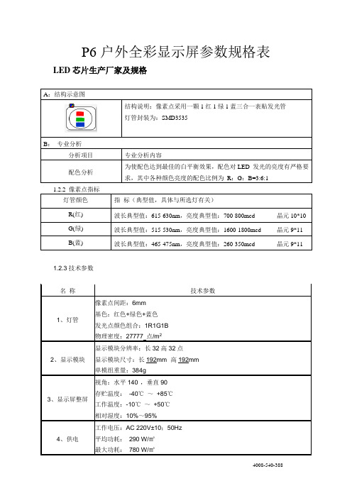
P6户外全彩显示屏参数规格表LED芯片生产厂家及规格
A:结构示意图
结构说明:像素点采用一颗1红1绿1蓝三合一表贴发光管
灯管封装为:SMD3535
B:专业分析
分析项目专业分析内容
配色分析为使配色达到最佳的白平衡效果,配色对LED 发光的亮度有严格要求,其中各种颜色亮度的配色比例为R:G:B=3:6:1
1.2.2 像素点指标
灯管颜色指标(典型值,具体与所选灯有关)
R(红) 波长典型值:615-630nm,亮度典型值:700-800mcd 晶元10*10 G(绿) 波长典型值:515-530nm,亮度典型值:1600-1800mcd 晶元9*11 B(蓝) 波长典型值:465-475nm,亮度典型值:260-350mcd 晶元9*11
1.2.3技术参数
名称技术参数
1、灯管像素点间距:6mm
基色:红色+绿色+蓝色
发光点颜色组合:1R1G1B 物理密度:27777 点/m2
2、显示模块显示模块分辨率:长32高32点
显示模块尺寸:长192mm×高192mm 单模组重量:384g
3、显示屏整屏视角:水平140°,垂直90°存贮温度:-40℃~+85℃工作温度:-10℃~+50℃相对湿度:10%~95%
4、供电工作电压:AC 220V±10;50Hz 平均功耗:290 W/㎡
最大功耗:780 W/㎡
P6户外全彩单元板图片展示。
MEMORY存储芯片STM8S003F3P6中文规格书
This is information on a product in full production.August 2018DS7147 Rev 10Value line, 16-MHz STM8S 8-bit MCU, 8-Kbyte Flash memory, 128-byte data EEPROM, 10-bit ADC, 3 timers, UART, SPI, I²CDatasheet - production dataFeaturesCore•16 MHz advanced STM8 core with Harvard architecture and 3-stage pipeline •Extended instruction setMemories•Program memory: 8 Kbyte Flash memory; data retention 20 years at 55 °C after 100 cycles •RAM: 1 Kbyte•Data memory: 128 bytes true data EEPROM;endurance up to 100 k write/erase cyclesClock, reset and supply management• 2.95 V to 5.5 V operating voltage•Flexible clock control, 4 master clock sources –Low-power crystal resonator oscillator –External clock input–Internal, user-trimmable 16 MHz RC –Internal low-power 128 kHz RC •Clock security system with clock monitor •Power management–Low-power modes (wait, active-halt, halt)–Switch-off peripheral clocks individually –Permanently active, low-consumption power-on and power-down resetInterrupt management•Nested interrupt controller with 32 interrupts •Up to 27 external interrupts on 6 vectorsTimers•Advanced control timer: 16-bit, 4 CAPCOM channels, 3 complementary outputs, dead-time insertion and flexible synchronization •16-bit general purpose timer, with 3 CAPCOM channels (IC, OC or PWM)•8-bit basic timer with 8-bit prescaler •Auto wakeup timer•Window and independent watchdog timersCommunications interfaces•UART with clock output for synchronousoperation, SmartCard, IrDA, LIN master mode •SPI interface up to 8 Mbit/s •I 2C interface up to 400 Kbit/sAnalog to digital converter (ADC)•10-bit ADC, ± 1 LSB ADC with up to 5multiplexed channels, scan mode and analog watchdogI/Os•Up to 28 I/Os on a 32-pin package including 21high-sink outputs •Highly robust I/O design, immune against current injectionDevelopment support•Embedded single-wire interface module(SWIM) for fast on-chip programming and non-intrusive debuggingDescription STM8S003F3 STM8S003K3DS7147 Rev 102 DescriptionThe STM8S003F3/K3 value line 8-bit microcontrollers offer 8 Kbytes of Flash programmemory, plus integrated true data EEPROM. They are referred to as low-density devices in the STM8S microcontroller family reference manual (RM0016).The STM8S003F3/K3 value line devices provide the following benefits: performance, robustness and reduced system cost.Device performance and robustness are ensured by true data EEPROM supporting up to 100000 write/erase cycles, advanced core and peripherals made in a state-of-the-arttechnology at 16 MHz clock frequency, robust I/Os, independent watchdogs with separate clock source, and a clock security system.The system cost is reduced thanks to a high system integration level with internal clock oscillators, watchdog, and brown-out reset.Full documentation is offered as well as a wide choice of development tools.Table 1. STM8S003F3/K3 value line featuresFeaturesSTM8S003K3STM8S003F3Pin count3220Max. number of GPIOs (I/O)2816External interrupt pins 2716Timer CAPCOM channels 77Timer complementary outputs 32A/D converter channels 45High-sink I/Os2112Low-density Flash program memory (byte)8 K 8 K RAM (byte)1 K 1 K True data EEPROM (byte)128(1)1.Without read-while-write capability.128(1)Peripheral setMulti purpose timer (TIM1), SPI, I2C, UART, Window WDG, independent WDG, ADC, PWM timer (TIM2), 8-bit timer (TIM4)DS7147 Rev 10STM8S003F3 STM8S003K3Block diagram3 Block diagramFigure 1. STM8S003F3/K3 value line block diagramXTAL 1-16 MHzRC int. 16 MHzRC int. 128 kHzSTM8 coreDebug/SWIMUART1I2CSPIAWU timerReset blockResetPORBORClock controllerDetectorClock to peripherals and core400Kbit/s8Mbit/sup to 5A d d r e s s a n d d a t a b u sWindow WDG8 Kbyte 128 byte 1 Kbyte RAMADC1ResetSingle wiredebug interfaceprogram Flashdata EEPROM16-bit general purpose16-bit advanced controltimer (TIM1)timer (TIM2)8-bit basic timer(TIM4)Beeper1/2/4 kHz beepIndependent WDG4 CAPCOM channels Up to 3 CAPCOM channelsUp to + 3 complementaryoutputsLIN master channelsSPI emul.STM8S003F3 STM8S003K3Product overviewDS7147 Rev 10Product overview STM8S003F3 STM8S003K3DS7147 Rev 104.12 TIM4 - 8-bit basic timer•8-bit autoreload, adjustable prescaler ratio to any power of 2 from 1 to 128•Clock source: CPU clock•Interrupt source: 1 x overflow/update4.13 Analog-to-digital converter (ADC1)STM8S003F3/K3 value line products contain a 10-bit successive approximation A/Dconverter (ADC1) with up to 5 external multiplexed input channels and the following main features: •Input voltage range: 0 to V DDA •Conversion time: 14 clock cycles•Single and continuous, buffered continuous conversion modes •Buffer size (10 x 10 bits)•Scan mode for single and continuous conversion of a sequence of channels •Analog watchdog capability with programmable upper and lower thresholds •Analog watchdog interrupt •External trigger input •Trigger from TIM1 TRGO •End of conversion (EOC) interruptNote:Additional AIN12 analog input is not selectable in ADC scan mode or with analog watchdog. Values converted from AIN12 are stored only into the ADC_DRH/ADC_DRL registers.4.14 Communication interfacesThe following communication interfaces are implemented:•UART1: full feature UART, synchronous mode, SPI master mode, SmartCard mode,IrDA mode, LIN2.1 master capability •SPI: full and half-duplex, 8 Mbit/s •I²C: up to 400 Kbit/sTable 3. TIM timer featuresTimerCounter size (bits)PrescalerCounting mode CAPCOM channels Complem. outputs Ext. trigger Timersynchr-onization/ chainingTIM1 16Any integer from 1 to 65536Up/down 43Yes NoTIM2 16Any power of 2 from 1 to 32768Up 30No TIM48Any power of 2 from 1 to 128UpNo。
- 1、下载文档前请自行甄别文档内容的完整性,平台不提供额外的编辑、内容补充、找答案等附加服务。
- 2、"仅部分预览"的文档,不可在线预览部分如存在完整性等问题,可反馈申请退款(可完整预览的文档不适用该条件!)。
- 3、如文档侵犯您的权益,请联系客服反馈,我们会尽快为您处理(人工客服工作时间:9:00-18:30)。
产品规格书
目录
目录 0
1. 适用范围 (1)
2. 产品说明 (1)
3. 产品参数 (2)
4. 信号引脚定义 (3)
5. 规格型号说明 (4)
6. IC贴片图 (4)
7. 安装孔位图 (5)
8. 室内P6.0八扫全彩表贴三拼一单元板备件 (7)
9. 产品使用注意事项 (7)
1. 适用范围
本技术手册仅适用于室内P6.0(32*16)八扫全彩表贴三拼一单元板。
2. 产品说明
2.1. 室内P6.0八扫全彩表贴三拼一单元板主要是由红色LED、绿色LED和蓝色LED
组成矩阵,然后再固定到塑胶套件上而成;
2.2. 此单元板含有驱动芯片和输入缓冲芯片,连接到LED显示屏控制系统即可显示
视频、图像和文字信息等;
2.3. 通过PWM信号驱动红色LED、绿色LED和蓝色LED的驱动芯片,可形成
16,777,216种颜色变换;
2.4. 此单元板可以按水平和垂直方向任意拼接,从而拼成不同大小的显示屏;
2.5. 单元板的特点:
●用超高亮的LED和优质的塑胶件
●高对比度可达到良好的显示效果
●重量轻易于安装、拆卸
●可进行单点、单灯维护,成本低
●采用恒流方式驱动LED,发光均匀,功耗低
●像素间距为6.0mm,共有32*16个像素点,每个像素点由1R1G1B组成
2.6. 单元板图片
正
视
图
背
视
图
3. 产品参数(温度条件:Ta=25℃)
4. 信号引脚定义
HUB75
5. 规格型号说明
产品型号命名规范:
6. IC 贴片图
7 B2 蓝色数据信号 8 GND 电源地 9 A 行电源控制信号 10 B 行电源控制信号 11 C 行电源控制信号 12 GND 电源地 13 CLK 时钟信号
14 LAT
数据锁存信号
15
OE
使能信号
16
GND 电源地
元器件 贴片位置 元器件 贴片位置 74HC245 U1-U2
74H138 U3 16126D UR1-UR4、UG1-UG4、UB1- UB4 4953 T1-T8 电阻391,390Ω
RR1-RR4、RG1-RG4、RB1-RB4
电容104
C1-C15
排阻560,56Ω RP1-RP8、RP13-RP20 (空白)
备注:VRR 、VRG 、VRB 为白平衡调节电阻,其阻值根据使用不同灯管的实际情况而定。
7. 安装孔位图
单元板安装孔位(如图1):
衬板安装孔位(如图2、3、4、5):
图3:2*1
图5:2*2
备注:
带底壳加衬板的衬板单元板总厚度为20.6mm;
所有尺寸的单位为mm;如无特殊说明,外形公差为±0.2,孔径公差为±0.1。
8. 室内P6.0八扫全彩表贴三拼一单元板备件
9. 产品使用注意事项
9.1. LED焊接。
使用烙铁人手焊接:
●推荐使用低于25W以下的烙铁,焊接时烙铁的温度必须保持在315℃以下,且每个电
极只能进行一次焊接,每次焊接的时间不得超过3秒;当第一次没有焊接好时,必须
停10S后才可以焊接;第二次没有焊接好时,必须更换新SMD灯。
开关电源外壳、箱体、屏体等严格接地;
●烙铁不能接触的环氧树脂部分;
●当焊接好之后,要让它冷却到温度低于40℃才可以包装;
9.2. LED清洗:
●不要使用不明化学液体清洗SMD LED,不明化学液体可能会损坏SMD LED;必要清
洗时,把SMD LED沉浸在酒精里,在正常的室温下少于1分钟并且自然干燥15分钟,
然后才开始使用;
●在焊接后推荐使用酒精进行清洗,在温度不高于30℃的条件下持续3分钟,不高于50℃
的条件下持续30秒。
使用其它类似溶剂清洁前,请先确认使用的溶剂不会对LED的封
装和环氧树脂部份造成损伤;
●超声波清洗也是有效的方法,一般最大功率不应超过300W,否则可能对LED造成损伤;
在使用前必须预先测试清洗条件是否会对LED造成损伤;不推荐使用;
9.3. LED防潮湿包装:
●为避免产品在运输及储存中吸湿,SMD LED的包装袋是用防潮的铝包装袋包装,并且
包装袋里面含有干燥剂,干燥剂主要起到控制包装袋里的湿度,湿度卡主要是起到监
控包装袋里的湿度;
9.4. LED贮存:
●本产品使用密封防潮抗静电袋包装,并附有干燥剂,未开封的产品有半年的保存时间。
当超过保持期时需要重新烘烤;
●开封前,产品须存放在温度不高于30℃,湿度不高于60%RH的环境中;
●开封后,产品须存放在温度不高于30℃,湿度不高于10%RH的环境中,且应该在168
小时(7天)内使用完;
●工作环境为温度不高于30℃,湿度不高于60%RH.在干燥的报季节必须在24小时用完,
在潮湿的季节必须在此12小时内用完,否则须做烘烤处理才可使用;
9.5. 静电:
●静电(ESD)和电涌(EOS)会导致产品特性发生改变,例如正向电压降低等,如果情况
严重甚至会损毁坏产品。
所以在使用时必须采取有效的防静电措施;
●所有相关的设备和机器都应该正确接地,同时必须采取其他防止静电和电涌的措施;
●使用防静电手环,防静电垫子,防静电工作服、工作鞋、手套,防静电容器,都是有
效的防止静电和电涌的措施;
9.6. 拿取:
●直接用手拿取产品不但会污染封装树脂表面,也可能由于静电等因素导致产品性能的
改变;过度的压力也可能直接影响封装内部的管芯和金线,因此请勿对产品施加过度
压力,特别当产品处于高温状态下,例如在回流焊接过程中;
9.7. 单元板
9.7.1批次标识:
●在整个生产过程中,单元板上须要有明确的批次标识;
9.7.2包装:
●老化好的产品包装应在温度小于30℃,湿度小于60%RH的环境下进行;
●每个纸箱应放入不低于500g的干燥剂或吸湿袋;
●考虑到囤货和回潮天气,包装应尽可能严实,避免直接与空气接触,最好能密封;
●箱体上要标明产品型号和生产批次号,不同批号的产品不能装在同一包装箱,否则用
到显示屏上将会产生色块(马赛克)现象;
9.7.3储存:
●包装好的产品应放在较为干燥的环境,湿度要控制在70%RH以下,特别是在霉雨天气,
仓库不能出现回潮;
●包装好的产品存放时间如果超过一个月,建议拿出来做2小时的老化后,再包装入库;
9.8. 显示屏
9.8.1显示屏拼装:
●一块显示屏体要选用同一批次的单元板。
如要用到2批次以上单元板,要上报到技术
部处理;
9.8.2使用注意:
●此类SMD显示屏不能使用在严重潮湿环境下,特别是在回潮天气产品的保存使用,如
显示屏的使用及储存不好,会造成LED灯烧死、暗亮、短路、开路和灯体损坏,并会
造成在显示屏上出现串亮情况;为提高显示屏及LED的产品使用寿命,请遵循以下使
用及储存方法,最好能将环境湿度控制在70%RH以下;
9.8.3固定类显示屏:
●建议在干燥的季节,每周最少要开显示屏1天;
●在60%~80%RH相对湿度范围内,建议每天最少要开显示1次,每次2小时以上来去除
显示屏上的湿气,时间最好为早上7点到10点之间或晚上6点到10点之间;
●如湿度高于80%RH或回潮天气,建议每天播放视频8H以上,并且晚上要关好相关门窗,
防止晚上回潮造成严重不良;特别是回潮天,建议有条件的可以24小时开机播放视屏;
9.8.4租赁屏显示屏:
●每次使用完之后,需立即装入航空箱,如显示屏上沾有水,必须将其吹干后方可放入,
并盖好航空箱盖;
●在每个航空箱内,请放入不低于500g的干燥剂或吸湿袋;
●在干燥的季节,每1个月最少取出1次播放视屏2H以上,在60%~80%RH相对湿度范
围内每半个月取出播放视频2H以上,超过80%RH和在回潮天气,每周必须取出放视频
2H以上,所有的播放完之后,需立即放放航空箱内,封好保存(请注意检查航空内干
燥剂或吸湿袋有无失效,另多放干燥剂可以提高箱内的干燥度,可以加长开箱开机烤
机的时间);
●出租使用时,不要有雨水沾到显示屏正面,如有水沾上,要尽快点亮显示屏,靠灯和
IC发热将雨水蒸发;。