ZR36420中文资料
Z5U0805HTTDB123Z中文资料(KOA)中文数据手册「EasyDatasheet - 矽搜」

472
5600 .0056
562
6800 .0068
682
8200 .0082
822
10000 .010
103
12000 .012
123
15000 .015
153
18000 .018
183
22000 .022
223
27000 .027
273
33000 .033
333
39000 .039
393
0402*
芯片中文手册,看全文,戳
特征
• 高Q值 • 低T.C.C. • 可在高电容值(高达100μF)
尺寸和建设
W t
d
电极
L
d
陶瓷 体
焊接 电镀(锡)
Ni
电镀
银 金属化
案件 尺寸
0402 0603 0805 1206 1210
L
.039±.004 (1.0±0.1)
.063±.006 (1.6±0.15)
以较低者为准
+ 25°C10,000MΩ分钟. 或1000MΩ - μF分钟.
以较低者为准
+ 25°C10,000MΩ分钟. 或1000MΩ - μF分钟.
以较低者为准
环境应用
绝缘电阻与温度.
NPO - 温度系数
X5R - 温度系数
X7R - 温度系数
Y5V - 温度系数
Z5U - 温度系数
芯片中文手册,看全文,戳
capacitors
订购信息
新零件#
NPO
介电
NPO X5R X7R Y5V Z5U
0805
尺寸
0402 0603 0805 1206 1210
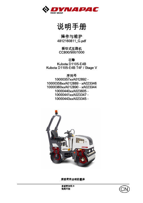
振动式压路机CC800 900 1000操作与维护说明手册说明书
2020-11-24
4812160811_G.pdf
生产能力.................................................................................................... 14 综合 ........................................................................................................... 15 二氧化碳排放量........................................................................................... 15 紧固扭矩.................................................................................................... 16 ROPS - 螺栓.............................................................................................. 17 液压系统.................................................................................................... 17 压路机说明 ............................................................................................................................. 19 柴油引擎.................................................................................................... 19 电气系统.................................................................................................... 19 推进系统/传动............................................................................................ 19 制动系统.................................................................................................... 19 转向系统.................................................................................................... 19 ROPS ........................................................................................................ 19 标识 ......................................................................................................................... 19 车架上的产品标识号.................................................................................. 20 压路机铭牌 ................................................................................................ 20 17PIN 序列号的说明.................................................................................. 21 引擎铭牌.................................................................................................... 21 标志牌...................................................................................................................... 22 位置 - 标志牌 ............................................................................................. 22 安全标志牌 ................................................................................................ 23 信息标志牌 ................................................................................................ 25 互锁/紧急停车/停车制动 - 检查.................................................................. 25 仪表/控件 ................................................................................................................. 26 位置 - 仪表和控件...................................................................................... 26 位置 - 控制面板和控件............................................................................... 27 功能说明.................................................................................................... 28 电气系统 .................................................................................................................. 30 熔断器 ....................................................................................................... 30 引擎舱中的熔断器 ..................................................................................... 31
23L6423A-70中文资料

FEATURES•Bit organization- 8M x 8 (byte mode)- 4M x 16 (word mode)•Fast access time- Random access:70ns (max.)- Page access:25ns (max.)•Page size- 8 words per page•Current- Operating:20mA- Standby:15uA•Supply voltage- 2.7V ~ 3.6V•Package- 48 pin TSOP (12mm x 20mm)•Temperature- 0°C ~ 70°C for commercial grade - -40°C ~ 85°C for industrial grade •Process- 0.18um PIN DESCRIPTIONSymbol Pin FunctionA0~A21Address InputsD0~D14Data OutputsD15/A-1D15 (Word Mode)/ LSB Address(Byte Mode)CE#Chip Enable InputOE#Output Enable InputByte#Word/ Byte Mode Selection VCC Power Supply PinVSS Ground PinNC No ConnectionPIN CONFIGURATION48 TSOP (Top View)MX23L6423A64M-BIT PAGE MODE MASK ROM A15A14A13A12A11A10A9A8A19A20NCNCA21NCNCA18A17A7A6A5A4A3A2A1123456789101112131415161718192021222324A16BYTE#VSSD15 /A-1D7D14D6D13D5D12D4VCCD11D3D10D2D9D1D8D0OE#VSSCE#A0484746454443424140393837363534333231302928272625ORDER INFORMATIONPart No.Speed Package Grade RemarkMX23L6423A TC-7070ns48 pin TSOP CommercialMX23L6423A TC-9090ns48 pin TSOP CommercialMX23L6423A TC-70G70ns48 pin TSOP Commercial Pb-freeMX23L6423A TC-90G90ns48 pin TSOP Commercial Pb-freeMX23L6423A TI-70G70ns48 pin TSOP Industrial Pb-freeMX23L6423A TI-90G90ns48 pin TSOP Industrial Pb-freeP/N:PM1179REV. 1.5 , APR. 15, 2005MX23L6423AABSOLUTE MAXIMUM RATINGSItemSymbol RatingsVoltage on any Pin Relative to VSS VIN -0.3V to 3.9V Ambient Operating T emperature T opr -40°C to 85°C Storage TemperatureTstg-65°C to 125°CDC CHARACTERISTICS (T a = -40°C ~ 85°C, VCC = 2.7V~3.6V)ItemSymbol MIN.MAX.Conditions Output High Voltage VOH 2.4V -IOH = -400uA Output Low Voltage VOL -0.4V IOL = 1.6mAInput High Voltage VIH 0.7xVCC VCC+0.3Input Low VoltageVIL -0.3V 0.8V Input Leakage Current ILI -5uA 0V, VCC Output Leakage Current ILO -5uA 0V, VCCOperating Current ICC -20mA f=5MHz, CE#=VIL, OE#=VIH all output open Standby Current (CMOS)ISTB -15uA CE#>VCC-0.2VInput Capacitance CIN -10pF Ta = 25°C, f = 1MHZ Output CapacitanceCOUT-10pFTa = 25°C, f = 1MHZNote:1. Output high-impedance delay (tHZ) is measured from OE# or CE# going high, and this parameter guaranteed by design over the full voltage and temperature operating range - not tested.MODE SELECTIONCE#OE#Byte#D15/A-1D0~D7D8~D15Mode Power H X X X High Z High Z -Stand-by L H X XHigh Z High Z -Active L L H Output D0~D7D8~D15Word Active LLLInputD0~D7High ZByteActiveAC CHARACTERISTICS (T a = -40°C ~ 85°C, VCC = 2.7V~3.6V)ItemSymbol 23L6423A-7023L6423A-90MIN.MAX.MIN.MAX.Read Cycle Time tRC 70ns -90ns -Address Access Time tAA -70ns -90ns Chip Enable Access Time tCE -70ns -90ns Page Access Time tPA -25ns -25ns Output Enable Time tOE -25ns -25ns Output Hold After Address tOH 0ns -0ns -Output High Z DelaytHZ-20ns-20nsMX23L6423A Array AC Test ConditionsInput Pulse Levels0V~ 3.0VInput Rise and Fall Times5nsInput Timing Level 1.5VOutput Timing Level 1.5VOutput Load See FigureNote:No output loading is present in tester load board.Active loading is used and under software programming control.Output loading capacitance includes load board's and all stray capacitance.TIMING DIAGRAMRANDOM READPAGE READMX23L6423A PACKAGE INFORMATIONMX23L6423AREVISION HISTORYRevision #Description Page Date1.1 1. Added access time : 70ns P1,2JAN/27/20052. Modified VIH(min.) from 2.2V to 0.7xVCC P21.2 1. Added Pb-free package information P1FEB/17/20052. Deleted access time:100ns P1,21.3 1. Added process:0.18um P1MAR/02/20051.4 1. Added Industrial Grade P1,2MAR/30/20051.5 1. Changed temperature from -25°C~85°C to -40°C~85°C P1,2APR/15/2005MX23L6423A M ACRONIX I NTERNATIONAL C O., L T D.Headquarters:TEL:+886-3-578-6688FAX:+886-3-563-2888Europe Office :TEL:+32-2-456-8020FAX:+32-2-456-8021Hong Kong Office :TEL:+86-755-834-335-79FAX:+86-755-834-380-78Japan Office :Kawasaki Office :TEL:+81-44-246-9100FAX:+81-44-246-9105Osaka Office :TEL:+81-6-4807-5460FAX:+81-6-4807-5461Singapore Office :TEL:+65-6346-5505FAX:+65-6348-8096Taipei Office :TEL:+886-2-2509-3300FAX:+886-2-2509-2200M ACRONIX A MERICA, I NC.TEL:+1-408-262-8887FAX:+1-408-262-8810http : //。
远东电缆参数表

聚氯乙烯绝缘电线(电缆)PVC Insulated Wire and Cables远东电缆有限公司FAR EAST CABLE CO,.LTD一.产品标准Standards产品按GB/T5023-2008/IEC60227《额定电压450/750V及以下聚氯乙烯绝缘电缆》、JB8734-1998《额定电压450/750V及以下聚氯乙烯绝缘电缆电线和软线》标准生产聚氯乙烯绝缘电线电缆,同时还可根据用户需要按国际电工委员会推荐标准IEC、英国标准、德国标准及美国标准生产.二.适用范围Applications本产品适用于工频额定电压U0/U 450/750V及以下动力、日用电器、仪器仪表及电信设备。
三.使用特性Operating characteristics●额定电压U0/U为450/750V、300/500V和300/300V。
●电缆导体的最高允许工作温度Max. admissible operating temperature of the conductors 60227IEC07(BV-90).......................... ..............90℃60227IEC08(RV-90).................. ......................90℃60227IEC56(RVV-90)........................ ...............90℃60227IEC57(RVV-90)........................................90℃其它型号 the other types.................................70℃●电缆敷设时环境温度应不低于0℃。
●电缆弯曲半径 The bending radius of cableD≤25mm........................................≥ 4 DD>25mm.........................................≥ 6 DType and description of the cable五.生产范围Production range of cable六.结构尺寸及主要技术参数Construction and main technical data60227 IEC 01 (BV)型60227 IEC 05 (BV)型60227 IEC 06 (RV)型导体标称截面mm2导体种类绝缘厚度mm平均外径mm 近似重量kg/km导体(铜)最大电阻20 ℃MΩ·km70℃时最小绝缘电阻MΩ·km下限上限不镀金属镀金属0.5 0.75 11.52.5 111110.60.60.60.70.81.92.12.22.63.22.32.52.73.23.98.0410.5513.2819.4130.7436.024.518.112.17.4136.724.818.212.27.560.0150.0130.0120.0110.00960227 IEC 08 (RV-90)型标称截面mm2导体种类绝缘厚度mm平均外径上限mm 近似重量kg/km导体(铜)最大电阻20 ℃MΩ·km 70℃时最小绝缘电阻MΩ·km不镀金属Non-metalplate镀金属Metalplate下限上限0.5 0.75 11.52.5 555550.60.60.60.70.82.12.22.42.83.42.52.72.83.44.18.3411.0813.7319.8830.9539.026.019.513.37.9840.126.720.013.78.210.0130.0120.0100.0090.009BV、BV-90 型与 RV、RV-90 型60227 IEC 10 (BVV)型60227 IEC 42 (RVB )型导体标称截面mm2导体种类绝缘厚度规定值mm平均外形尺寸20℃时导体(铜)最大电阻70℃时最小绝缘电阻MΩ·km参考重量kg/km下限mm上限mm不镀金属镀金属0.5 0.75 660.80.82.5×5.02.7×5.43.0×6.03.2×6.439.026.040.126.70.0160.01420.4026.0960227 IEC 52 (RVV)型导体标称截面mm2导体种类绝缘厚度规定值mm护套厚度规定值mm平均外形尺寸20℃时导体(铜)最大电阻70℃时最小绝缘电阻MΩ·km参考重量kg/km下限mm上限mm不镀金属镀金属2×0.52×0.753×0.5 3×0.75 5555550.50.50.50.50.50.50.60.60.60.60.60.64.63.0×4.94.93.2×5.24.95.25.93.7×5.96.33.8×6.36.36.739.039.026.026.019.519.540.140.126.726.720.020.00.0120.0120.0100.0100.0120.01039.1624.8246.8631.0449.7060.4560227 IEC 53 (RVV)型导体标称截面mm2导体种类绝缘厚度规定值mm护套厚度规定值mm平均外形尺寸20℃时导体(铜)最大电阻70℃时最小绝缘电阻MΩ·km参考重量kg/km下限mm上限mm不镀金属镀金属2×0.752×12×1.5 2×2.5 *2×4 *2×6 555555550.60.60.60.60.70.80.80.80.80.80.80.80.81.01.11.25.73.7×6.05.93.9×6.26.88.410.312.57.24.5×7.27.54.7×7.58.6010.612.414.626.026.019.519.513.37.984.953.3026.726.720.020.013.78.215.093.390.0110.0110.0100.0100.0100.0090.0070.00649.2439.3456.5945.7474.60113.45159.13224.88*16×1 *16×1.5 *16×2.5 *16×4 *16×6 *19×0.75 *19×1 *19×1.5 *19×2.5 *19×4 *19×6 *24×0.75 *24×1 *24×1.5 *24×2.5 *24×4 *24×6 555555555555555550.60.70.80.80.80.60.60.70.80.80.80.60.60.70.80.80.81.21.41.71.71.71.51.51.71.71.71.81.21.31.41.51.71.713.316.119.121.926.613.113.916.720.523.128.116.017.020.324.127.233.516.319.122.125.530.216.317.119.923.726.931.919.220.223.527.331.037.319.513.37.984.953.3026.019.513.37.984.953.3026.019.513.37.984.953.3020.013.78.215.093.3926.720.013.78.215.093.3926.720.013.78.215.093.390.0100.0100.0090.0070.0060.0110.0100.0100.0090.0070.0060.0110.0100.0100.0090.0070.006300.67436.64638.98937.641319.83289.10345.34493.43756.981086.281532.84384.99457.68648.44952.111369.821953.4760227 IEC 56 (RVV-90)型导体标称截面mm2导体种类绝缘厚度规定值mm护套厚度规定值mm平均外形尺寸20℃时导体(铜)最大电阻70℃时最小绝缘电阻MΩ·km参考重量kg/km下限mm上限mm不镀金属镀金属2×0.52×0.753×0.5 3×0.75 5555550.50.50.50.50.50.50.60.60.60.60.60.64.63.0×4.94.93.2×5.24.95.25.93.7×5.96.33.8×6.36.36.739.039.026.026.019.519.540.140.126.726.720.020.00.0120.0120.0100.0100.0120.01039.1624.8246.8631.0449.7060.4560227 IEC 57(RVV-90)型导体标称截面mm2导体种类绝缘厚度规定值mm护套厚度规定值mm平均外形尺寸20℃时导体(铜)最大电阻70℃时最小绝缘电阻MΩ·km参考重量kg/km下限mm上限mm不镀金属镀金属2×0.75 2×1 55550.60.60.60.60.80.80.80.85.73.7×6.05.93.9×6.27.24.5×7.27.54.7×7.526.026.019.519.526.726.720.020.00.0110.0110.0100.01049.2439.3456.5945.74BV型300/500V 铜芯聚氯乙烯绝缘电线导体标称截面mm2绞合导体中单线最少根数Min绝缘厚度规定值mm平均外径上限mm20℃时导体电阻最大值Ω/km70℃时最小绝缘电阻MΩ·km参考重量kg/km铜芯copperconductor镀锡铜芯tinnedcopperconductor0.75 1 770.60.62.62.824.518.124.818.20.0140.01311.1513.99BLV型450/750V铜芯聚氯乙烯绝缘电缆导体标称截面mm2实心导体或绞合导体中单线最少根数绝缘厚度规定值mm平均外径上限mm20℃时导体电阻最大值Ω/km70℃时最小绝缘电阻MΩ·km参考重量kg/km*1.5 2.5 4 6 10 16 25 35 50 70 95 120 150 185 240 300 400 *500 *630 1111777719191937373761616161910.70.80.80.81.01.01.21.21.41.41.61.61.82.02.22.42.62.83.03.43.94.45.06.77.89.710.912.814.617.118.820.923.326.629.633.236.640.8-12.17.414.613.081.911.200.8680.6410.4430.3200.2530.2060.1640.1250.1000.0778---0.0100.00850.00700.00650.00500.00500.00400.00450.00350.00350.00320.00320.00320.00320.00300.0028--10.2215.5121.1328.2749.9370.80110.24143.30193.85263.29362.46440.93545.00683.20886.251105.541397.911743.562183.94 BVR型450/750V铜芯聚氯乙烯绝缘软电缆导体标称截面mm2绞合导体中单线最少根数绝缘厚度规定值mm平均外径上限mm20℃时导体电阻最大值Ω/km70℃时最小绝缘电阻MΩ·km参考重量kg/km铜芯镀锡铜芯2.5 4 6 10 16 19191949490.80.80.81.01.04.14.85.36.88.17.414.613.081.831.157.564.703.111.841.160.0110.0090.00840.00720.006232.1247.5768.48121.35174.5825 35 50 70 *95 *120 *150 *185 *2409813313318925925970370312201.21.21.41.41.61.61.82.02.210.211.713.916.018.119.822.425.027.80.7270.5240.3870.268-----0.7340.5290.3910.270-----0.00580.00520.00510.0045-----285.52376.73517.43719.28979.001206.141523.931895.952390.60 BVV型300/500V铜芯聚氯乙烯绝缘聚氯乙烯护套圆形电缆标称截面mm2实心导体或绞合导体中单线最少根数绝缘厚度规定值mm护套厚度规定值mm平均外径上限mm20℃时导体电阻最大值Ω/km70℃时最小绝缘电阻MΩ·km参考重量kg/km下限lowerlimit上限Upperlimit铜芯copperconductor镀锡铜芯tinnedcopperconductor0.751.01.52.5 2.5 4 4 6 6 10 11117171770.60.60.70.80.80.80.80.80.81.00.80.80.80.80.80.90.90.90.90.93.63.74.24.84.85.45.55.96.07.34.44.55.05.75.96.56.87.17.38.824.518.112.17.417.414.614.613.083.081.8324.818.212.27.567.564.704.703.113.111.840.0120.0110.0110.0100.0090.00850.00770.00700.00650.006520.8724.1631.8545.2647.9863.9766.8585.3288.70140.14 BLVV型300/500V铝芯聚氯乙烯绝缘聚氯乙烯护套圆形电缆主要技术参数标称截面Nom.cross sectional area of conductormm2实心导体或绞合导体中单线最少根数Min number of thesingle wire in solidor flexibleconductor绝缘厚度规定值Thick ofinsulationsettedmm护套厚度规定值Thick ofsheathsettedmm平均外径averagediametermm20℃时导体电阻最大值Max.resistanced.c. of conductorat 20 ℃Ω/km70℃时最小绝缘电阻Min resistanceof insulationat 70℃MΩ·km参考重量Referencedweightkg/km下限lowerlimit上限Upperlimit0.751.01.52.5 4 6 10 11111170.60.60.70.80.80.81.00.80.80.80.80.90.90.93.63.74.24.85.45.97.34.44.55.05.76.57.18.8---12.17.414.613.080.0120.0110.0110.0100.00850.00700.006516.3017.9822.6630.0439.7148.8477.11B V V B、B L V V B型300/500V铜、铝芯聚氯乙烯绝缘聚氯乙烯护套扁形电缆主要技术参数芯数×标称截面Nom.cross sectional area of conductormm2实心导体或绞合导体中单线最少根数Min number ofthe single wirein solid orflexibleconductor绝缘厚度规定值Thick ofinsulation settedmm护套厚度规定值Thick ofsheathsettedmm平均外径average diametermm20℃时导体电阻最大值Max.resistance d.c. ofconductor at 20 ℃Ω/km70℃时最小绝缘电阻Minresistance ofinsulation at70℃MΩ·km参考重量Referencedweightkg/km下限lowerlimit上限Upperlimit铜芯Cucore镀锡铜芯tinnedCucore铝芯AlcoreBVVB BLVVB2×0.75 2×1.0 2×1.5 2×2.5 2×4 2×4 2×6 2×6 2×10 3×0.75 3×1.0 3×1.5 3×2.5 3×4 3×4 3×6 3×6 3×101111171771111171770.60.60.70.80.80.80.80.81.00.60.60.70.80.80.80.80.81.00.90.90.91.01.01.01.11.11.20.90.90.91.01.11.11.11.11.23.8×5.93.9×6.14.4×7.05.1×8.45.6×9.25.6×9.26.2×10.46.2×10.47.9×13.43.8×7.93.9×8.44.4×9.65.1×11.65.8×13.15.8×13.16.2×14.56.2×14.57.9×19.04.6×7.14.8×7.45.3×8.56.2×10.16.7×11.16.7×11.17.5×12.57.5×12.59.5×16.24.6×9.64.8×10.15.3×11.76.2×14.07.0×15.87.0×15.87.8×18.27.8×18.29.5×23.024.518.112.17.414.614.613.083.081.8324.518.112.17.414.614.613.083.081.8324.818.212.27.564.704.703.113.111.8424.818.212.27.564.704.703.113.111.84---12.17.41-4.61-3.08---12.17.41-4.61-3.080.0120.0110.0110.0100.00850.0080.00700.00650.00650.0120.0110.0110.0100.00850.0080.00700.00650.006538.5144.9960.1288.43122.53128.06168.88175.63281.4455.2163.9686.32127.79183.07191.41246.64256.44412.9029.3732.6341.7557.9873.9977.8195.91100.75155.1541.5145.4158.7682.11110.26116.03137.19144.11223.47RVS 型300/300V铜芯聚氯乙烯绝缘绞型连接用软电线主要技术参数芯数×标称截面Nom.cross sectional area of conductormm2导体中单线最大直径Max diameter ofthe single wire inconductormm绝缘厚度规定值Thick ofinsulationsettedmm平均外径上限Upper limit ofaverage diamm20℃时导体电阻最大值Max.resistance d.c. ofconductor at 20 ℃Ω/km70℃时最小绝缘电阻Min resistance ofinsulation at70℃MΩ·km参考重量Referencedweightkg/km铜芯coppercore镀锡铜芯tinnedcoppercore2×0.5 0.16 0.8 6.0 39.0 40.1 0.016 22.032×0.75 0.16 0.8 6.2 26.0 26.7 0.014 28.18 RVP、RVP-90型300/300V铜芯聚氯乙烯绝缘屏蔽软电缆主要技术参数芯数×标称截面Nom.cross sectional area of conductormm2导体中单线最大直径Max diameter ofthe single wirein conductormm绝缘厚度规定值Thick ofinsulationsettedmm屏蔽层单线直径diameter ofthe singlewire in screenmm平均外径或外形尺寸上限Upper limit ofaveragediametermm20℃时导体电阻最大值Max.resistanced.c. of conductorat 20 ℃Ω/km70℃时最小绝缘电阻Min resistanceof insulationat 70℃MΩ·km参考重量Referencedweightkg/km铜芯coppercore镀锡铜芯tinnedcoppercore1×0.08 1×0.12 1×0.2 1×0.3 1×0.4 1×0.5 1×0.75 1×1.0 1×1.5 1×2.5 *1×4 *1×6 2×0.08 2×0.12 2×0.2 2×0.3 2×0.4 2×0.5 2×0.75 2×1.0 2×1.5 *2×2.5 *2×4 0.130.160.160.160.160.210.210.210.260.260.310.310.130.160.160.160.160.210.210.210.260.260.310.40.40.40.50.50.50.50.60.60.70.80.80.40.40.40.50.50.50.50.60.60.70.80.100.100.100.100.150.150.150.150.150.150.150.150.100.100.100.150.150.150.150.150.150.150.151.92.02.22.63.03.13.43.84.14.95.76.73.33.53.94.85.25.46.06.87.48.710.224715892.369.248.239.026.019.513.37.98--24715892.369.248.239.026.019.513.3--25416395.071.249.640.126.720.013.78.21--25416395.071.249.640.126.720.013.7--0.0180.0160.0130.0140.0130.0120.0100.0100.0090.008--0.0180.0160.0130.0140.0130.0120.0100.0100.009--5.015.777.159.3011.0012.3515.4619.9625.5542.4062.4384.1711.7513.5016.6626.3630.5833.8841.3652.7866.03101.66141.18RVVP型300/300V铜芯聚氯乙烯绝缘屏蔽聚氯乙烯护套软电缆主要技术参数芯数×标称截面Nom.cross sectional area of conductormm2导体中单线最大直径Max diameterof thesingle wirein conductormm绝缘厚度规定值Thick ofinsulation settedmm屏蔽层单线直径diameterof thesinglewire inscreenmm护套厚度规定值Thick ofsheathsettedmm平均外径或外形尺寸Upper limit ofaverage diametermm20℃时导体电阻最大值Max.resistanced.c. of conductorat 20 ℃Ω/km70℃时最小绝缘电阻Min resistanceof insulationat 70℃MΩ·km参考重量Referencedweightkg/km下限lowerlimit上限Upperlimit铜芯coppercore镀锡铜芯tinnedcoppercore1×0.3 1×0.4 1×0.5 1×0.75 1×1.0 1×1.5 1×2.5 *1×4 *1×6 2×0.32×0.42×0.52×0.752×1.02×1.5*2×2.5*2×43×0.3 3×0.4 3×0.5 3×0.75 3×1.0 0.160.160.210.210.210.260.260.310.310.160.160.210.210.210.260.260.310.160.160.210.210.210.50.50.50.50.60.60.70.80.80.50.50.50.50.60.60.70.80.50.50.50.50.60.100.100.100.100.100.100.150.150.150.150.150.150.150.150.150.150.150.150.150.150.150.150.40.40.40.40.60.60.60.80.80.60.60.60.60.60.81.01.00.60.60.60.60.82.93.03.13.44.14.34.96.07.14.83.5×5.15.13.6×5.45.33.7×5.65.84.0×6.16.44.3×6.77.34.9×7.69.06.0×9.310.47.1×10.75.15.45.66.13.53.73.84.14.95.26.07.18.26.24.2×6.26.64.4×6.66.84.5×6.87.44.8×7.48.25.2×8.39.26.0×9.310.97.1×11.011.58.2×11.66.56.97.169.248.239.026.019.513.37.98--69.2-48.2-39.0-26.0-19.5-13.3-7.98---69.248.239.026.019.571.249.640.126.720.013.78.21--71.2-49.6-40.1-26.7-20.0-13.7-8.21---71.249.640.126.720.00.0140.0130.0120.0100.0100.0090.008--0.014-0.013-0.012-0.010-0.010-0.009-0.008---0.0140.0130.0120.0100.01014.4616.4417.9921.5030.2536.6455.9283.60107.5440.1635.7045.1940.0949.0543.4857.6851.1171.2262.6892.9082.07143.53125.84188.10165.4946.6553.1558.2069.6293.67七.载流量 Current carrying capacity固定敷设用单芯聚氯乙烯绝缘电线连续负荷载流量(A)Current carrying capacity of single core PVC insulation cables for fixed wiring注:1)电缆相互接触2)相邻电缆中心距离为2倍电缆外径固定敷设用单芯聚氯乙烯绝缘电线连续负荷载流量(A)Current carrying capacity of single core PVC insulation cables for fixed wiring注:1)电缆相互接触2)相邻电缆中心距离为2倍电缆外径连接用聚氯乙烯绝缘软电缆(电线)连续负荷载流量(A)Current carrying capacity of PVC insulation flexible cables (cords) for connecting注:1)电缆相互接触2)相邻电缆中心距离为2倍电缆外径3)电缆分离敷设。
SSC-MGT6423中文资料

5. Rank of MGT722
▣ Rank Name Table X1 Iv X2 λd X3 Vf
▣ Luminous Intensity [Iv] Rank Iv (mcd) Name MIN MAX N 1000 1600 O 1600 2000 P 2000 2500 ▣ Dominant Wavelength [λd] Rank λd (nm) Name MIN MAX 519 525 A 525 531 B C 531 537 ▣ Forward Voltage Rank Name 1 2 3 Vf (V) MIN 2.7 3.1 3.6 MAX 3.1 3.6 4.1
4. Electro-Optical Characteristics
Parameter Forward Voltage (per die) Reverse Current (per die) Luminance Intensity *1 Dominant Wavelength
Peak Wavelength
SSC-QP-7-03-08(REV.07)
SEOUL SEMICONDUCTOR CO., LTD. 148-29 Kasan-Dong, Keumchun-Gu, Seoul, 153-023, Korea Phone : 82-2-2106-7305~6
SSC-MGT722
- 2/10 -
元器件交易网
∆λ
2 θ½
IF =60 mA IF =60 mA
-
20 120
-
nm deg
*1 The luminous intensity IV was measured at the peak of the spatial pattern which may not be aligned with the mechanical axis of the LED package. Luminous Intensity Measurement allowance is ±10%. *2 2θ½ is the off-axis where the luminous intensity is 1/2 of the peak intensity. [Note] All measurements were made under the standardized environment of SSC.
RE030024中文资料
General Purpose Relays
Miniature PCB Relay RE
I I I I I I I I
1 pole 6 A, 1NO contact Sensitive coil 200 mW 4 kV coil-contact Optimized height 10,6 mm PCB area 200 mm2 Wash tight Plastic materials according to IEC60335-1 (domestic appliances) RoHS compliant (Directive 2002/95/EC) as per product date code 0352
Contact data
Contact configuration Contact set Type of interruption Rated current Rated voltage / max.switching voltage AC Maximum breaking capacity AC Limiting making capacity, max 4 s, duty factor 10% Contact material Mechanical endurance Rated frequency of operation with / without load Contact Type RE030 RE030 RE030 RE034 1 NO single contact micro disconnection 6A 240/400 VAC 1500 VA 15 A AgCdO AgNi0.15 and AgNi90/10 >30x106 cycles 6/1200 min-1
AO6420中文资料

SymbolTyp Max 4862.574110R θJL 3540Maximum Junction-to-Lead CSteady-State°C/WThermal Characteristics ParameterUnits Maximum Junction-to-Ambient A t ≤ 10s R θJA °C/W Maximum Junction-to-Ambient A Steady-State °C/W AO6420AO6420SymbolMin TypMaxUnits BV DSS 60V 1T J =55°C5I GSS 100nA V GS(th)1 2.33V I D(ON)20A 5060T J =125°C856075m Ωg FS 13S V SD 0.781V I S3A C iss 450540pF C oss 60pF C rss 25pF R g1.652ΩQ g (10V)9.511.5nC Q g (4.5V) 4.3 5.5nC Q gs 1.6nC Q gd 2.2nC t D(on) 5.17ns t r 2.64ns t D(off)15.920ns t f 23ns t rr 25.135ns Q rr28.7nCTHIS PRODUCT HAS BEEN DESIGNED AND QUALIFIED FOR THE CONSUMER MARKET. APPLICATIONS OR USES AS CRITICAL COMPONENTS IN LIFE SUPPORT DEVICES OR SYSTEMS ARE NOT AUTHORIZED. AOS DOES NOT ASSUME ANY LIABILITY ARISING OUT OF SUCH APPLICATIONS OR USES OF ITS PRODUCTS. AOS RESERVES THE RIGHT TO IMPROVE PRODUCT DESIGN,FUNCTIONS AND RELIABILITY WITHOUT NOTICEMaximum Body-Diode Continuous CurrentDYNAMIC PARAMETERS Body Diode Reverse Recovery ChargeTotal Gate Charge I F =4.2A, dI/dt=100A/µsTurn-Off DelayTime Turn-Off Fall TimeBody Diode Reverse Recovery Time I F =4.2A, dI/dt=100A/µs Input Capacitance N Channel Electrical Characteristics (T J =25°C unless otherwise noted)ParameterConditions STATIC PARAMETERS Drain-Source Breakdown Voltage I D =250µA, V GS =0V I DSS Zero Gate Voltage Drain Current V DS =60V, V GS =0VµA Gate-Body leakage current V DS =0V, V GS = ±20V Gate Threshold Voltage V DS =V GS I D =250µA On state drain currentV GS =10V, V DS =5V R DS(ON)Static Drain-Source On-ResistanceForward Transconductancem ΩV GS =4.5V, I D =3AV DS =5V, I D =4.2AI S =1A,V GS =0V V GS =10V, I D =4.2ADiode Forward VoltageV GS =10V, V DS =30V, R L =7Ω, R GEN =3ΩGate Source Charge Gate Drain Charge Turn-On DelayTime Turn-On Rise Time Total Gate Charge V GS =10V, V DS =30V, I D =4.2AV GS =0V, V DS =30V, f=1MHz V GS =0V, V DS =0V, f=1MHzSWITCHING PARAMETERS Reverse Transfer Capacitance Gate resistanceOutput Capacitance A: The value of R θJA is measured with the device mounted on 1in 2FR-4 board with 2oz. Copper, in a still air environment with T A =25°C. The value in any given application depends on the user's specific board design. The current rating is based on the t ≤ 10s thermal resistance rating.B: Repetitive rating, pulse width limited by junction temperature.C. The R θJA is the sum of the thermal impedence from junction to lead R θJL and lead to ambient.D. The static characteristics in Figures 1 to 6 are obtained using <300 µs pulses, duty cycle 0.5% max.E. These tests are performed with the device mounted on 1 in 2FR-4 board with 2oz. Copper, in a still air environment with T A =25°C. The SOA curve provides a single pulse rating.F.The current rating is based on the t ≤ 10s thermal resistance rating.Rev0: Feb. 2007AO6420AO6420。
LTC6420-20资料

1642020faFEATURESAPPLICATIONSDESCRIPTION1.8GHz Differential Amplifi ers/ADC Drivers The L TC ®6420-20 is a dual high-speed differential amplifi er targeted at processing signals from DC to 300MHz. The part has been specifi cally designed to drive 12-, 14- and 16-bit ADCs with low noise and low distortion, but can also be used as a general-purpose broadband gain block.The L TC6420-20 is easy to use, with minimal support circuitry required. The output common mode voltage is set using an external pin, independent of the inputs, which eliminates the need for transformers or AC-coupling capacitors in many applications. The gain is internally fi xed at 20dB (10V/V).The L TC6420-20 saves space and power compared to alternative solutions using IF gain blocks and transformers. The LTC6420-20 is packaged in a compact 20-lead 3mm × 4mm QFN package and operates over the –40°C to 85°C temperature range.Distribution of Gain MatchnMatched Gain ±0.1dBn Matched Phase ±0.1° at 100MHz n Channel Separation 80dB at 100MHzn 1.8GHz –3dB Bandwidth; Fixed Gain of 10V/V (20dB)n IMD3 = –84dBc at 100MHz, 2V P-P n Equivalent OIP3 = 46dBm at 100MHz n 1nV/√Hz Internal Op Amp Noise n 6.2dB Noise Figuren Differential Inputs and Outputs n Rail-to-Rail Output Swingn 80mA Supply Current (240mW) per Amplifi er n 1.1V to 1.6V Output Common Mode Voltage, Adjustablen DC- or AC-Coupled Operation n 20-Lead 3mm × 4mm × 0.75mm QFN PackagenDifferential ADC Driver n Differential Driver/Receivern Single Ended to Differential Conversion n IF Sampling (Diversity) ReceiversMatched Dual Amplifi er with Output Common Mode BiasingL , L T , L TC and L TM are registered trademarks of Linear Technology Corporation. All other trademarks are the property of their respective owners.T YPICAL APPLICATION 642020 TA01aV OCM AV OCM AV OCM BV OCM B±0.1dB GAIN MATCHING±0.1° PHASE MATCHING AT 100MHzV IN AV IN BCHANNEL-TO-CHANNEL GAIN MATCH (dB)–0.25U N I T S (%)403530152025105–0.15–0.05642020 TA01b0.050.150.252642020faABSOLUTE MAXIMUM RATINGSSupply Voltage (V + – V –) .........................................3.6V Input Current (Note 2) ..........................................±10mA Operating Temperature Range (Note 3)...–40°C to 85°C Specifi ed Temperature Range (Note 4) ....–40°C to 85°C Storage Temperature Range ...................–65°C to 150°C Maximum Junction Temperature...........................150°C Output Short Circuit Duration...........................Indefi nite(Note 1)2019181778TOP VIEW21UDC PACKAGE20-LEAD (3mm s 4mm) PLASTIC QFN910654321111213141516+INA –INA V –V ––INB +INB –OUTA V + AV –V –V + B –OUTBV + AV O C M AE N A B L E A+O U T AV + BV O C M BE N A B L E B+O U T BT JMAX = 150°C, θJA = 43°C/W , θJC = 5°C/WEXPOSED PAD (PIN 21) IS V –, MUST BE SOLDERED TO PCBORDER INFORMATIONPART NUMBER GAIN(dB)GAIN (V/V)Z IN (DIFFERENTIAL)(Ω)SINGLE DUALCOMMENT L TC6400-88 2.5400Lowest Distortion L TC6400-14145200Lowest Distortion L TC6400-20 L TC6420-202010200Lowest Distortion L TC6400-26262050Lowest Distortion L TC6401-88 2.5400Lowest Power L TC6401-14145200Lowest Power L TC6401-20 L TC6421-202010200Lowest Power L TC6401-26262050Lowest PowerPIN CONFIGURATIONLEAD FREE FINISH TAPE AND REEL PART MARKING*PACKAGE DESCRIPTIONSPECIFIED TEMPERATURE RANGE L TC6420CUDC-20#PBF L TC6420CUDC-20#TRPBF LDDM20-Lead (3mm × 4mm) Plastic QFN 0°C to 70°C L TC6420IUDC-20#PBFL TC6420IUDC-20#TRPBFLDDM20-Lead (3mm × 4mm) Plastic QFN–40°C to 85°CConsult L TC Marketing for parts specifi ed with wider operating temperature ranges. *The temperature grade is identifi ed by a label on the shipping container .Consult L TC Marketing for information on non-standard lead based fi nish parts.For more information on lead free part marking, go to: http://www.linear .com/leadfree/ For more information on tape and reel specifi cations, go to: http://www.linear .com/tapeandreel/SELECTOR GUIDEDC ELECTRICAL CHARACTERISTICSSYMBOL PARAMETER CONDITIONS MIN TYP MAX UNITS Input/Output CharacteristicG DIFF Gain V IN = ±100mV Differential l19.62020.4dB ΔG Gain Matching Channel-to-Channel l±0.1±0.25dB TC GAIN Gain Temperature Drift V IN = ±100mV Differential l0.0015dB/°C V SWINGMIN Output Swing Low (V OCM = 1.5V)Each Output, V IN = ±400mV Differential l0.20.35V V SWINGMAX Output Swing High (V OCM = 1.5V)Each Output, V IN = ±400mV Differential l 2.65 2.8V V OUTDIFFMAX Maximum Differential Output Swing l 4.6 5.2V P-P I OUT Output Current Drive2V P-P, OUT (Note 10)l20mA V OS Input Offset Voltage Differential l–2±0.42mV TCV OS Input Offset Voltage Drift Differential l 1.2μV/°C I VRMIN Input Common Mode Voltage Range, MIN l1V I VRMAX Input Common Mode Voltage Range, MAX l 1.6V R INDIFF Input Resistance (+IN, –IN)Differential l170200230ΩΔR IN Input Impedance Matching Channel-to-Channel l±0.5±2.5% C INDIFF Input Capacitance (+IN, –IN)Differential, Includes Parasitic1pF R OUTDIFF Output Resistance (+OUT, –OUT)Differential l202536ΩCMRR Common Mode Rejection Ratio Input Common Mode Voltage 1V to 1.6V l4568dB Output Common Mode Voltage ControlG CM Common Mode Gain V OCM = 1.1V to 1.6V1V/V V OCMMIN Output Common Mode Range, MIN l 1.1V V OCMMAX Output Common Mode Range, MAX l 1.6V V OSCM Common Mode Offset Voltage V OCM = 1.25V to 1.5V l–10±210mV TCV OSCM Common Mode Offset Voltage Drift l16μV/°C IV OCM V OCM Input Current l–15–30μA ENABLE x Pins (x = A, B)V IL ENABLEx Input Low Voltage l0.8V V IH ENABLEx Input High Voltage l 2.4VENABLEx Input Current ENABLEx ≤ 0.8VENABLEx ≥ 2.4V ll 1.5±0.54μAμAPower SupplyV S Operating Supply Range l 2.853 3.5V I S Supply Current ENABLEx≤ 0.8V; per Amplifi er l8095mA I SHDN Shutdown Supply Current ENABLEx≥ 2.4V; per Amplifi er. Inputs Floating l13mAPSRR Power Supply Rejection Ratio (DifferentialOutputs)V+ = 2.85V to 3.5V l5586dBThel denotes the specifi cations which apply over the full operating temperature range, otherwise specifi cations are at T A = 25°C. V+ = 3V, V– = 0V, +IN = –IN = V OCM = 1.25V, ENABLE = 0V, No R L unless otherwise noted.3642020faAC ELECTRICAL CHARACTERISTICSThel denotes the specifi cations which apply over the full operating temperature range, otherwise specifi cations are at T A = 25°C. V+ = 3V, V– = 0V, V OCM = 1.25V, ENABLE = 0V, No R L unless otherwise noted. SYMBOL PARAMETER CONDITIONS MIN TYP MAX UNITS ΔG Gain Matching f = 100MHz (Note 9)l±0.1±0.25dB ΔP Phase Matching f = 100MHz±0.1deg Channel Separation (Note 8) f = 100MHz80dB –3dBBW–3dB Bandwidth200mV P-P,OUT (Note 6) 1.8GHz 0.5dBBW Bandwidth for 0.5dB Flatness200mV P-P,OUT (Note 6)0.7GHz 0.1dBBW Bandwidth for 0.1dB Flatness200mV P-P,OUT (Note 6)0.3GHz NF Noise Figure R L = 375Ω (Note 5), f = 100MHz 6.2dB e IN Input Referred Voltage Noise Density Includes Resistors (Short Inputs), f = 100MHz 2.2nV/√Hz e ON Output Referred Voltage Noise Density Includes Resistors (Short Inputs), f = 100MHz22nV/√Hz 1/f1/f Noise Corner10kHz SR Slew Rate Differential (Note 6)4500V/μs t S1%1% Settling Time2V P-P,OUT (Note 6)0.8ns t OVDR Overdrive Recovery Time 1.9V P-P,OUT (Note 6): Single Ended4ns P1dB1dB Compression Point R L = 375Ω (Notes 5, 7), f = 100MHz18dBm t ON Turn-On Time+OUT, –OUT Within 10% of Final Values82ns t OFF Turn-Off Time I CC Falls to 10% of Nominal190ns –3dBBW VOCM V OCM Pin Small Signal –3dB BW0.1V P-P at V OCM, Measured Single-Ended atOutput (Note 6)15MHzIMD33rd Order Intermodulation Distortion f = 100MHz (1MHz Spacing)V OUT = 2V P-P Composite–84dBc OIP33rd Order Output Intercept f = 100MHz (Note 7)46dBmIIP33rd Order Input Intercept f = 100MHz (Z IN = 50Ω)f = 100MHz (Z IN = 200Ω)2620dBmdBmHD22nd Order Harmonic Distortion f = 100MHz; V OUT = 2V P-P–80dBc HD33rd Order Harmonic Distortion f = 100MHz; V OUT = 2V P-P–88dBcNote 1: Stresses beyond those listed under Absolute Maximum Ratings may cause permanent damage to the device. Exposure to any Absolute Maximum Rating condition for extended periods may affect device reliability and lifetime.Note 2: Input pins (+IN, –IN) are protected by steering diodes to either supply. If the inputs go beyond either supply rail, the input current should be limited to less than 10mA.Note 3: The L TC6420C and L TC6420I are guaranteed functional over the operating temperature range of –40°C to 85°C.Note 4: The L TC6420C is guaranteed to meet specifi ed performance from 0°C to 70°C. It is designed, characterized and expected to meet specifi ed performance from –40°C to 85°C but is not tested or QA sampled at these temperatures. The L TC6420I is guaranteed to meet specifi ed performance from –40°C to 85°C.Note 5: Input and output baluns used. See Test Circuit A.Note 6: Measured using Test Circuit B. R L = 87.5Ω on each output.Note 7: Since the L TC6420-20 is a feedback amplifi er with low output impedance, a resistive load is not required when driving an AD converter. Therefore, typical output power is very small. In order to compare theL TC6420-20 with amplifi ers that require 50Ω output load, the output voltage swing driving a given R L is converted to OIP3 and P1dB as if it were driving a 50Ω load. Using this modifi ed convention, 2V P-P is by defi nition equal to 10dBm, regardless of actual R L.Note 8: Channel separation (the inverse of crosstalk) is measured by driving a signal into one input, while terminating the other input. Channel separation is the ratio of the resulting output signal at the driven channel to the channel that is not driven.Note 9: Not production tested. Guaranteed by design and by correlation to production tested parameters.Note 10: The output swing range is at least 2V P-P differential even when sourcing or sinking 20mA. Tested at V OCM = 1.5V.4642020fa5642020faFREQUENCY (MHz)P H A S E (D E G R E E )–100–200–300–400GROUP DELAY (ns)1.20.90.60.302004006008001000642020 G05FREQUENCY (MHz)1010010003000G A I N (d B )252015105642020 G04Frequency ResponseS21 Phase and Group Delay vs FrequencyInput and Output Refl ection and Reverse Isolation vs FrequencyFREQUENCY (MHz)10S P A R A M E T E R S (d B )0–10–20–30–40–50–60–70–8010010003000642020 G06FREQUENCY (MHz)1I M P E D A N C E M A G N I T U D E (Ω)250200150100500PHASE (DEGREES)503010–10–30–50101001000642020 G07Input and Output Impedance vs FrequencyTYPICAL PERFORMANCE CHARACTERISTICSChannel to Channel Gain Match vs FrequencyChannel to Channel Group Delay Match vs FrequencyChannel to Channel Phase Match vs FrequencyFREQUENCY (MHz)1010010002000G A I N M A T C H (d B )0.50.40.00.20.10.3–0.1–0.4–0.3–0.2–0.5642020 G01FREQUENCY (MHz)1010010002000G R O U P D E L A Y M A T C H (n s e c )0.50.40.00.20.10.3–0.1–0.4–0.3–0.2–0.5642020 G02FREQUENCY (MHz)101001000P H A S E M A T C H (d e g )0.50.40.00.20.10.3–0.1–0.4–0.3–0.2–0.5642020 G036642020faTYPICAL PERFORMANCE CHARACTERISTICSFREQUENCY (MHz)10N O I S E F I G U R E (d B )1510241214680113513791INPUT REFERRED NOISE VOL TAGE (nV/√Hz )64201001000642020 G08Noise Figure and Input Referred Noise Voltage vs FrequencyTIME (ns)0O U T P U T V O L T A G E (V )2.50.51.02.01.550100150200642020 G10Overdrive Transient ResponseTIME (ns)0O U T P U T V O L T A G E (V )1.351.201.251.301.15246810642020 G09Small Signal Transient ResponseFREQUENCY (MHz)T H I R D O R D E R I M D (d B c )–40–50–60–80–90–70–110–100642020 G1250100150200250300Third Order Intermodulation Distortion vs FrequencyFREQUENCY (MHz)O U T P U T I P 3 (d B m )6050402010300642020 G1350100150200250300Equivalent Output Third Order Intercept vs FrequencyChannel Separation vs Frequency (Note 8)Harmonic Distortion vs FrequencyFREQUENCY (MHz)50H A R M O N I C D I S T O R T I O N (d B c )–40–50–60–80–90–70–100100150200250300642020 G11FREQUENCY (MHz)C H A N N E L S E P A R A T I O N (d B )642020 G141201002040608001100100010PIN FUNCTIONS+INA, –INA, –INB, +INB (Pins 1, 2, 5, 6): Differential Inputs of A and B channel respectively.V– (Pins 3, 4, 13, 14, 21): Negative Power Supply. All four pins, as well as the exposed back, must be connected to same voltage/ground.ENABLEA, ENABLEB (Pins 9, 18): Logic inputs. If low, the amplifi er is enabled. If high, the amplifi er is disabled and placed in a low power shutdown mode, making the amplifier outputs high impedance. These pins are internally separate. These pins should not be left fl oating.V+ A, V+ B (Pins 15, 20, 7, 12 ): Positive Power Supply (Normally tied to 3V or 3.3V). Supply pins of A and B channels are internally separate. Bypass each pin with 1000pF and 0.1μF capacitors as close to the pins as possible.–OUTA, +OUTA, –OUTB, +OUTB (Pins 16, 17, 11, 10): Differential Outputs of channels A and B respectively.V OCMA, V OCMB (Pins 19, 8): These pins set the output common mode voltage for the respective channel. They are internally separate. A 0.1μF external bypass capacitor is recommended.Exposed Pad (Pin 21): V–. The Exposed Pad must be connected to same voltage/ground as pins 3, 4, 13, 14.BLOCK DIAGRAMV BV+BV+A–OUTA–OUTB V OCMB+INA –INAV–V–V–V–++OUTB–INB+INB7642020fa8642020faAPPLICATIONS INFORMATIONFigure 1. Input Termination for Differential 50Ω Input Impedance Using Shunt ResistorFigure 2. Input Termination for Differential 50Ω Input Impedance Using a 1:4 BalunFigure 3. Input Termination for Single-Ended 50Ω Input ImpedanceCircuit OperationEach of the two channels of the L TC6420-20 is composed of a fully differential amplifi er with on chip feedback and output common mode voltage control circuitry. Differential gain and input impedance are set by 100Ω/1000Ω resistors in the feedback network. Small output resistors of 12.5Ω improve the circuit stability over various load conditions.The L TC6420-20 is very fl exible in terms of I/O coupling. It can be AC- or DC-coupled at the inputs, the outputs or both. If the inputs are AC-coupled, the input common mode voltage is automatically biased close to V OCM and thus no external circuitry is needed for bias. The L TC6420-20 provides an output common mode voltage set by V OCM , which allows driving an ADC directly without external components such as a transformer or AC coupling capacitors. The input signal can be either single-ended or differential with only minordifferences in distortion performance.Input Impedance and MatchingThe differential input impedance of the L TC6420-20 is 200Ω. If a 200Ω source impedance is unavailable, then the differential inputs may need to be terminated to a lower value impedance, e.g. 50Ω, in order to provide an impedance match for the source. Several choices are avail-able. One approach is to use a differential shunt resistor (Figure 1). Another approach is to employ a wide band transformer (F igure 2). Both methods provide a wide band impedance match. The termination resistor or the transformer must be placed close to the input pins in order to minimize the refl ection due to input mismatch. Alternatively, one could apply a narrowband impedance match at the inputs of the L TC6420-20 for frequency selection and/or noise reduction.Referring to Figure 3, L TC6420-20 can be easily confi gured for single-ended input and differential output without a balun. The signal is fed to one of the inputs through amatching network while the other input is connected to the same matching network and a source resistor. Because the return ratios of the two feedback paths are equal, the two outputs have the same gain and thus symmetrical swing. In general, the single-ended input impedance and termination resistor R T are determined by the combination of R S, R G and R F. For example, when R S is 50Ω, it is found that the single-ended input impedance is 202Ω and R T is 66.5Ω in order to match to a 50Ω source impedance.The LTC6420-20 is unconditionally stable. However, the overall differential gain is affected by both source impedance and load impedance as follows:A V=V OUTV IN=2000R S+200•R L25+R LOutput Impedance MatchThe L TC6420-20 can drive an ADC directly without external output impedance matching. Alternatively, the differential output impedance of 25Ω can be matched to a higher value impedance, e.g. 50Ω, by series resistors or an LC network.Output Common Mode AdjustmentThe output common mode voltage is set by the V OCM pin, which is a high impedance input. The output common mode voltage is capable of tracking V OCM in a range from 1.1V to 1.6V. The bandwidth of V OCM control is typically 15MHz, which is dominated by a low pass fi lter connected to the V OCM pin and is aimed to reduce common mode noise generation at the outputs. The internal common mode feedback loop has a –3dB bandwidth of 300MHz, allowing fast rejection of any common mode output voltage disturbance. The V OCM pin should be tied to a DC bias voltage with a 0.1μF bypass capacitor. When interfacing with A/D converters such as the L TC22xx families, the V OCM pin can be connected to the V CM pin of the ADC.Driving A/D ConvertersThe L TC6420-20 has been specifi cally designed to interface directly with high speed A/D converters. The back page of this data sheet shows the L TC6420-20 driving an L TC2285, which is a dual 14-bit, 125Msps ADC.The V OCM pins of the L TC6420-20 are connected to the V CM pins of the L TC2285, which provide a DC voltage level of 1.5V. Both ICs are powered from the same 3V supply voltage.The inputs to the L TC6420-20 can be confi gured in various ways, as described in the Input Impedance and Matching section of this data sheet. The outputs of the L TC6420-20 may be connected directly to the analog inputs of an ADC, or a simple lowpass or bandpass fi lter network may be inserted to reduce out-of-band noise.Test CircuitsDue to the fully-differential design of the L TC6420 and its usefulness in applications with differing characteristic specifi cations, two test circuits are used to generate the information in this data sheet. Test Circuit A is DC1299, a two-port demonstration circuit for the L TC6420/L TC6421 family. The schematic and silkscreen are shown in F igure 4. This circuit includes input and output transformers (baluns) for single-ended-to-differential conversion and impedance transformation, allowing direct hook-up to a 2-port network analyzer. There are also series resistors at the output to avoid loading the amplifi er directly with a 50Ω load. Due to the input and output transformers, the –3dB bandwidth is reduced from 1.8GHz to approximately 1.3GHz.Test Circuit B uses a 4-port network analyzer to measure S-parameters and gain/phase response. This removes the effects of the wideband baluns and associated circuitry, for a true picture of the >1GHz S-parameters and AC characteristics.APPLICATIONS INFORMATION9642020fa10642020faAPPLICATIONS INFORMATIONFigure 4a. Top Silkscreen of DC1299, Test Circuit A+INA–INA–INB+INB+V V VLTC6420-2011642020faInformation furnished by Linear Technology Corporation is believed to be accurate and reliable. However , no responsibility is assumed for its use. Linear Technology Corporation makes no representa-tion that the interconnection of its circuits as described herein will not infringe on existing patent rights.TYPICAL APPLICATIONSTest Circuit B, 4-Port Measurements (Only the Signal-Path Connections Are Shown)Parallel ADC Drivers to Reduce Wideband NoisePACKAGE DESCRIPTIONUDC Package20-Lead Plastic QFN (3mm × 4mm)(Reference LTC DWG # 05-08-1742 Rev Ø)NOTE:1. DRAWING IS NOT A JEDEC PACKAGE OUTLINE2. DRAWING NOT TO SCALE3. ALL DIMENSIONS ARE IN MILLIMETERS4. DIMENSIONS OF EXPOSED PAD ON BOTTOM OF PACKAGE DO NOT INCLUDEMOLD FLASH. MOLD FLASH, IF PRESENT, SHALL NOT EXCEED 0.15mm ON ANY SIDE 5. EXPOSED PAD SHALL BE SOLDER PLATED6. SHADED AREA IS ONLY A REFERENCE FOR PIN 1 LOCATION ON THE TOP AND BOTTOM OF PACKAGEBOTTOM VIEW—EXPOSED PADPIN 1 NOTCH RECOMMENDED SOLDER PAD PITCH AND DIMENSIONS APPLY SOLDER MASK TO AREAS THAT ARE NOT SOLDEREDLTC6420-2012642020faLinear Technology Corporation1630 McCarthy Blvd., Milpitas, CA 95035-7417(408) 432-1900 ● FAX: (408) 434-0507 ● LINEAR TECHNOLOGY CORPORA TION 2008LT 1008 REV A • PRINTED IN USATYPICAL APPLICATIONPART NUMBER DESCRIPTIONCOMMENTSHigh-Speed Differential Amplifi ers/Differential Op AmpsL T ®1993-2800MHz Differential Amplifi er/ADC Driver A V = 2V/V, OIP3 = 38dBm at 70MHz L T1993-4900MHz Differential Amplifi er/ADC Driver A V = 4V/V, OIP3 = 40dBm at 70MHz L T1993-10700MHz Differential Amplifi er/ADC Driver A V = 10V/V, OIP3 = 40dBm at 70MHzL T1994Low Noise, Low Distortion Differential Op Amp 16-Bit SNR and SFDR at 1MHz, Rail-to-Rail OutputsL T5514Ultralow Distortion IF Amplifi er/ADC Driver with Digitally Controlled GainOIP3 = 47dBm at 100MHz, Gain Control Range 10.5dB to 33dB L T5524Low Distortion IF Amplifi er/ADC Driver with Digitally Controlled GainOIP3 = 40dBm at 100MHz, Gain Control Range 4.5dB to 37dB L T6402-6300MHz Differential Amplifi er/ADC Driver A V = 6dB, Distortion < –80dBc at 25MHz L T6402-12300MHz Differential Amplifi er/ADC Driver A V = 12dB, Distortion < –80dBc at 25MHz L T6402-20300MHz Differential Amplifi er/ADC DriverA V = 20dB, Distortion < –80dBc at 25MHzL T6411Low Power Differential ADC Driver/Dual Selectable Gain Amplifi er 16mA Supply Current, IMD3 = –83dBc at 70MHz, A V = 1, –1 or 2L TC6400-20, L TC6400-26Low Noise, Low Distortion, Differential ADC Drivers A V = 20dB, 26dB; Single Amplifi er per IC, High Performance L TC6401-8,L TC6401-14L TC6401-20, L TC6401-26Low Noise, Low Distortion, Differential ADC DriversA V = 8dB, 14dB, 20dB, 26dB; Single Amplifi er per IC, Low PowerL TC6404-1Low Noise Rail-to-Rail Output Differential Amplifi er/ADC Driver 1.5nV/√Hz , –92dB Distortion at 10MHzL TC64063GHz Rail-to-Rail Input Differential Op Amp1.6nV/√Hz Noise, –72dBc Distortion at 50MHz, 18mAR ELATED PARTS Dual ADC Driver for Wideband Direct-Conversion Receivers642020 TA04–3dB FIL TER BANDWIDTH = 140MHz。
- 1、下载文档前请自行甄别文档内容的完整性,平台不提供额外的编辑、内容补充、找答案等附加服务。
- 2、"仅部分预览"的文档,不可在线预览部分如存在完整性等问题,可反馈申请退款(可完整预览的文档不适用该条件!)。
- 3、如文档侵犯您的权益,请联系客服反馈,我们会尽快为您处理(人工客服工作时间:9:00-18:30)。
ZR36420Zoran Corporation n 3112 Scott Blvd. n Santa Clara, CA 95054 n (408) 991-4111 main n (408) 991-4122 fax n PRODUCT BRIEF OverviewZoran's COACH-LC is the third generation Camera On A CHip (COACH) digital still camera processor, following the COACH and COACH-XL processors. COACH-LC is highly compatible with COACH and COACH-XL. All processors share the same devicedrivers and hardware interfaces. User interface software can also be reused across all three processors.COACH-LC is a complete solution for digital still camera designs. It includes all required hardware and microcode to support: progressive and interlaced CCD sensors, CMOSCOACH-LCsensors, View-LCD display, Eye-LCD display, TV output, Flash Memory, USB interface, RS232 interface and stereo audio recording/playback.COACH-LC is a cost effective, yet highly powerfuldigital still camera processor. Its architecture is flexible enough to support a wide range of camera designs, from low cost, low-resolution cameras up to high performance professional cameras with real-time high resolution image processing. User Interface software can be implemented within the COACH-LC (reducing theoverall camera cost) or via an external micro-controller.The COACH-LC comes with a complete development package that includes a set of software tools, PC drivers and a reference design platform. Camera System Block DiagramFeatures§ Direct glueless interface to industry standardCCD sensors from Sony, Sharp, and Matsushita (progressive and interlaced), and to several CMOS sensors.§ Supports image resolutions of up to 2.3Megapixels.§ Advanced CCD signal processing:o Quantization noise shapingo Color de-mosaic with aliasing reduction o Color space conversion o Image scalero Automatic White Balance (AWB) o Automatic Exposure (AE) o CCD noise suppression o Contrast enhancement o Edge enhancement§ Support for flash strobe light control, includingred-eye reduction.§ Direct interface to resident flash memory and/orremovable flash memory cards: CompactFlash (CF) and SmartMedia (SSFDC) and others. § Supports 16, 32, 64, 128Mbit SDRAM framebuffers (depending on the sensor resolutions). § Serial Communication Port for RS-232 and IrDAinterface.§ USB interface, including on-chip USB linedrivers.§ Real-time JPEG compression with advanced bitrate control ensures superior visual quality for the required number of stored images.§ Capture sequence of still images at 15 imagesper second.§ Movie (AVI) capture and playback to the Flashcard§ Video Capture Mode - capture CIF at 30 framesper second or VGA at 15 frames per second real-time video (MJPEG compressed) to a PC via USB.§ Audio codec support, allows for MP3 stereoplayback and audio annotation of pictures. § User interface implemented within the COACH-LC, no need for an additional microcontroller. § Analog and digital LCD, direct interface to Eye-LCD.§ NTSC/PAL encoder provides direct analogoutput to a TV monitor.§ DCF compliant, DPOF support, EXIF 2.1 imageand audio file format§ Font-based and graphics-based OSD (OnScreen Display) engines for displaying user-interface messages, menus and icons on the LCD/TV.§ Image enhancement & processing algorithms,e.g., image sharpening, image smoothing, and superposition of images for improved viewing and printing quality.§ Programmable DSP engine ensures seamlessupgrades through downloadable firmware. § Advanced power management.§ 256-pin MQFP & 280-pin BGA packages.DIGITAL CAMERA PROCESSORAugust 2000 ZR36420LC-PB-1.1Evaluation and Development Tools:§ Data Book - complete specifications anddescription of the COACH§ COACHWare high-level API - for host softwareimplementation of the user-interface§ FontMapMaker - for font map and icon creation § CAM-ON II - DSC reference design - completecamera system hardware§ USB PC drivers development kits (Win98) - forimage transfer and real-time video captureCamera System Block DiagramFor More Information:U.S. Headquarters Israel OperationsJapanChinaTaiwanTorontoZoran Corporation Zoran Microelectronics Ltd. Zoran Japan Office Zoran China Office Zoran Taiwan Office Zoran Toronto Labs 3112 Scott BlvdAdvanced Technology Ctr. 2-2-8 Roppongi, Suite 25073F, No. 425-12175 Queen St. East Santa Clara, CA 95054 USA P.O. Box 2495 Minato-kuElectronics Science & Tech Bldg.Jen Ai Road, Sec. 4 Suite 302 Tel: +1 (408) 919- 4111 Haifa, 31024 Israel Tokyo 106-0032, Japan 2070 Central Shennan Rd Taipei, Taiwan Toronto, OntarioFax: +1 (408) 919- 4122Tel: +972-4-854-5777 Tel: +81-03-5574-7081 Shenzhen, Guangdong Tel: +886-2-2721-5616 Canada Fax: +972-4-855-1550 Fax: +81-03-5574-7156 518031, P.R. China Fax: +886-2-2721-1488 M4E 1E5 Tel: +86-755-3780319 Tel: +1 (416) 690-335Fax: +86-755-3780852Fax: +1 (416) 690-336。