FCN2416A104K-D1中文资料
FM24系列中文资料
引脚说明
串行时钟信号引脚(SCL):在 SCL 输入时钟信号的上升 沿将数据送入 EEPROM 器件,并在时钟的下降沿将数 据读出。
串行数据输入/输出引脚(SDA):SDA 引脚可实现双 向串行数据传输。该引脚为开漏输出,可与其它多个 开漏输出器件或开集电极器件线或连接。
器件/页 地址脚(A2,A1,A0):A2、A1 和 A0 引脚 为 FM24C02 的硬件连接的器件地址输入引脚。在一 个总线上最多可寻址八个 2K 器件。(器件寻址详见器 件寻址章节内容) 。
FM24C08
FM24C08A
全地址(4K)
正常读写 正常读写
全地址(8K)
FM24C16 高半区(8K)
存储器结构
FM24C02,2K 串行电可擦除存储器:内部分为 32 页, FM24C08(A),8K 串行电可擦除存储器:内部分为 64
每页 8 字节,以 8 位地址寻址。
页,每页 16 字节,以 10 位地址寻址。
SCL WP VCC GND NC
引脚功能
器件地址输入 串行数据输入输出 串行时钟输入 写保护 电源 地 不连接
FM24C02/04/08(A)/16 两线制串行 EEPROM
版本 2.2
技术手册
3
图 1.结构框图
FM24C02/04/08(A)/16 两线制串行 EEPROM
版本 2.2
技术手册
版本 2.2
技术手册
6
交流参数
推荐参数的适用工作条件:TA = -40°C ~ +85°C,VCC = +2.2V ~ +5.5V,CL = 1 TTL Gate and 100 pF(除非 另有说明)。测试条件参见“注 2”。
UT-S3C2416开发板硬件手册
深圳市友坚恒天科技有限公司
版本记录
版本号 V1.0 V1.1
作者 Seeky Sturtle
版本说明 初始版本 细节修改
日期 2009-11-29 2010-05-24
深圳市友坚恒天科技有限公司
目录 ..................................................................................................................................................3
第五章 启动配置说明 ..................................................................................................................19
第六章 硬件设计原理和接口定义说明.......................................................................................21
第三章 结构框图 ..........................................................................................................................14
第四章 电源设计 ..........................................................................................................................15
MX25L1605DM2I-12G中文资料
16M-BIT [x 1 / x 2] CMOS SERIAL FLASH 32M-BIT [x 1 / x 2] CMOS SERIAL FLASH 64M-BIT [x 1 / x 2] CMOS SERIAL FLASHFEATURESGENERAL• Serial Peripheral Interface compatible -- Mode 0 and Mode 3• 16M:16,777,216 x 1 bit structure or 8,388,608 x 2 bits (two I/O read mode) structure 32M:33,554,432 x 1 bit structure or 16,772,216 x 2 bits (two I/O read mode) structure 64M:67,108,864 x 1 bit structure or 33,554,432 x 2 bits (two I/O read mode) structure • 512 Equal Sectors with 4K byte each (16Mb)1024 Equal Sectors with 4K byte each (32Mb)2048 Equal Sectors with 4K byte each (64Mb)- Any Sector can be erased individually•32 Equal Blocks with 64K byte each (16Mb)64 Equal Blocks with 64K byte each (32Mb)128 Equal Blocks with 64K byte each (64Mb)- Any Block can be erased individually • Single Power Supply Operation- 2.7 to 3.6 volt for read, erase, and program operations • Latch-up protected to 100mA from -1V to Vcc +1V • Low Vcc write inhibit is from 1.5V to 2.5VPERFORMANCE • High Performance- Fast access time: 86MHz serial clock (15pF + 1TTL Load) and 66MHz serial clock (30pF + 1TTL Load)- Serial clock of two I/O read mode : 50MHz (15pF + TTL Load), which is equivalent to 100MHz - Fast program time: 1.4ms(typ.) and 5ms(max.)/page (256-byte per page)- Byte program time: 9us (typical)- Continuously program mode (automatically increase address under word program mode)- Fast erase time: 60ms(typ.) /sector (4K-byte per sector) ; 0.7s(typ.) /block (64K-byte per block); 14s(typ.) /chip for 16Mb, 25s(typ.) for 32Mb, and 50s(typ.) for 64Mb • Low Power Consumption- Low active read current: 25mA(max.) at 86MHz, 20mA(max.) at 66MHz and 10mA(max.) at 33MHz - Low active programming current: 20mA (max.)- Low active erase current: 20mA (max.)- Low standby current: 20uA (max.)- Deep power-down mode 1uA (typical)• Typical 100,000 erase/program cyclesSOFTWARE FEATURES • Input Data Format- 1-byte Command code •Advanced Security Features - Block lock protectionThe BP0-BP3 status bit defines the size of the area to be software protection against program and erase instructions - Additional 512-bit secured OTP for unique identifier • Auto Erase and Auto Program Algorithm- Automatically erases and verifies data at selected sector- Automatically programs and verifies data at selected page by an internal algorithm that automatically times the program pulse widths (Any page to be programed should have page in the erased state first)MX25L1605D MX25L3205D MX25L6405D元器件交易网•Status Register Feature•Electronic Identification- JEDEC 1-byte manufacturer ID and 2-byte device ID- RES command for 1-byte Device ID- Both REMS and REMS2 commands for 1-byte manufacturer ID and 1-byte device IDHARDWARE FEATURES• SCLK Input- Serial clock input• SI Input- Serial Data Input• SO Output- Serial Data Output• WP#/ACC pin- Hardware write protection and program/erase acceleration• HOLD# pin- pause the chip without diselecting the chip• PACKAGE- 16-pin SOP (300mil)- 8-land WSON (8x6mm or 6x5mm)- 8-pin SOP (200mil, 150mil)- 8-pin PDIP (300mil)- 8-land USON (4x4mm)- All Pb-free devices are RoHS CompliantALTERNATIVE• Security Serial Flash (MX25L1615D/MX25L3215D/MX25L6415D) may provides additional protection features for op-tion. The datasheet is provided under NDA.GENERAL DESCRIPTIONThe MX25L1605D are 16,777,216 bit serial Flash memory, which is configured as 2,097,152 x 8 internally. When it is in two I/O read mode, the structure becomes 8,388,608 bits x 2. The MX25L3205D are 33,554,432 bit serial Flash memory, which is configured as 4,194,304 x 8 internally. When it is in two I/O read mode, the structure becomes 16,772,216 bits x 2. The MX25L6405D are 67,108,864 bit serial Flash memory, which is configured as 8,388,608 x 8 internally. When it is in two I/O read mode, the structure becomes 33,554,432 bits x 2. (please refer to the "Two I/O Read mode" section). The MX25L1605D/3205D/6405D feature a serial peripheral interface and software protocol allowing operation on a simple 3-wire bus. The three bus signals are a clock input (SCLK), a serial data input (SI), and a serial data output (SO). Serial access to the device is enabled by CS# input.When it is in two I/O read mode, the SI pin and SO pin become SIO0 pin and SIO1 pin for address/dummy bits input and data output.The MX25L1605D/3205D/6405D provides sequential read operation on whole chip.After program/erase command is issued, auto program/ erase algorithms which program/ erase and verify the specified page or sector/block locations will be executed. Program command is executed on byte basis, or page (256 bytes) basis, or word basis for Continuously program mode, and erase command is executes on sector (4K-byte), or block (64K-byte), or whole chip basis.To provide user with ease of interface, a status register is included to indicate the status of the chip. The status read command can be issued to detect completion status of a program or erase operation via WIP bit.Advanced security features enhance the protection and security functions, please see security features section for more details.When the device is not in operation and CS# is high, it is put in standby mode and draws less than 20uA DC current. The MX25L1605D/3205D/6405D utilizes MXIC's proprietary memory cell, which reliably stores memory contents even after typical 100,000 program and erase cycles.Table 1. Additional Feature ComparisonPIN CONFIGURATIONSSYMBOL DESCRIPTION CS#Chip SelectSI/SIO0Serial Data Input (for 1 x I/O)/ Serial Data Input & Output (for 2xI/O read mode)SO/SIO1Serial Data Output (for 1 x I/O)/ Serial Data Input & Output (for 2xI/O read mode)SCLK Clock InputWP#/ACCWrite protection: connect to GND ;9.5~10.5V for program/eraseacceleration: connect to 9.5~10.5V HOLD#Hold, to pause the device without deselecting the device VCC + 3.3V Power Supply GNDGroundPIN DESCRIPTION16-PIN SOP (300mil)8-LAND WSON (8x6mm, 6x5mm), USON (4x4mm)8-PIN SOP (200mil, 150mil)PACKAGE OPTIONS16M 32M 64M150mil 8-SOP V 200mil 8-SOP V V 300mil 16-SOP V V V300mil 8-PDIP V V 6x5mm WSON V V 8x6mm WSON V4x4mm USONVV12345678HOLD#VCC NC NC NC NC CS#SO/SIO1161514131211109SCLK SI/SIO0NC NC NC NC GND WP#/ACCCS#SO/SIO1WP#/ACCGND VCC HOLD#SCLK SI/SIO0CS#SO/SIO1WP#/ACC GND VCC HOLD#SCLK SI/SIO01234CS#SO/SIO1WP#/ACC GND 8765VCC HOLD#SCLK SI/SIO08-PIN PDIP (300mil)BLOCK DIAGRAMDATA PROTECTIONThe MX25L1605D/3205D/6405D is designed to offer protection against accidental erasure or programming caused by spurious system level signals that may exist during power transition. During power up the device automatically resets the state machine in the Read mode. In addition, with its control register architecture, alteration of the memory contents only occurs after successful completion of specific command sequences. The device also incorporates several features to prevent inadvertent write cycles resulting from VCC power-up and power-down transition or system noise.•Power-on reset and tPUW: to avoid sudden power switch by system power supply transition, the power-on reset and tPUW (internal timer) may protect the Flash.• Valid command length checking: The command length will be checked whether it is at byte base and completed on byte boundary.• Write Enable (WREN) command: WREN command is required to set the Write Enable Latch bit (WEL) before other command to change data. The WEL bit will return to reset stage under following situation:- Power-up- Write Disable (WRDI) command completion- Write Status Register (WRSR) command completion- Page Program (PP) command completion- Continuously Program mode (CP) instruction completion- Sector Erase (SE) command completion- Block Erase (BE) command completion- Chip Erase (CE) command completion- Write Read-lock Bit (WRLB) instruction completion•Deep Power Down Mode: By entering deep power down mode, the flash device also is under protected from writing all commands except Release from deep power down mode command (RDP) and Read Electronic Signature command (RES).•Advanced Security Features: there are some protection and securuity features which protect content from inadvertent write and hostile access.I. Block lock protection- The Software Protected Mode (SPM) use (BP3, BP2, BP1, BP0) bits to allow part of memory to be protected as read only. The proected area definition is shown as table of "Protected Area Sizes", the protected areas are more flexible which may protect various area by setting value of BP0-BP3 bits.Please refer to table of "protected area sizes".- The Hardware Proteced Mode (HPM) use WP#/ACC to protect the (BP3, BP2, BP1, BP0) bits and SRWD bit.Table 2. Protected Area SizesII. Additional 512-bit secured OTP for unique identifier: to provide 512-bit one-time program area for setting device unique serial number - Which may be set by factory or system customer. Please refer to table 3. 512-bit secured OTP definition.- Security register bit 0 indicates whether the chip is locked by factory or not.- To program the 512-bit secured OTP by entering 512-bit secured OTP mode (with ENSO command), and going through normal program procedure, and then exiting 512-bit secured OTP mode by writing EXSO command.- Customer may lock-down the customer lockable secured OTP by writing WRSCUR(write security register) command to set customer lock-down bit1 as "1". Please refer to table of "security register definition" for security register bit definition and table of "512-bit secured OTP definition" for address range definition.- Note: Once lock-down whatever by factory or customer, it cannot be changed any more. While in 512-bit secured OTP mode, array access is not allowed.Table 3. 512-bit Secured OTP DefinitionAddress range Size Standard Customer LockFactory Lockxxxx00~xxxx0F128-bit ESN (electrical serial number)Determined by customer xxxx10~xxxx3F384-bit N/AHOLD FEATURESHOLD# pin signal goes low to hold any serial communications with the device. The HOLD feature will not stop the operation of write status register, programming, or erasing in progress.The operation of HOLD requires Chip Select(CS#) keeping low and starts on falling edge of HOLD# pin signal while Serial Clock (SCLK) signal is being low (if Serial Clock signal is not being low, HOLD operation will not start until Serial Clock signal being low). The HOLD condition ends on the rising edge of HOLD# pin signal while Serial Clock(SCLK) signal is being low( if Serial Clock signal is not being low, HOLD operation will not end until Serial Clock being low), see Figure 1. Figure 1. Hold Condition OperationThe Serial Data Output (SO) is high impedance, both Serial Data Input (SI) and Serial Clock (SCLK) are don't care during the HOLD operation. If Chip Select (CS#) drives high during HOLD operation, it will reset the internal logic of the device. To re-start communication with chip, the HOLD# must be at high and CS# must be at low.PROGRAM/ERASE ACCELERATIONTo activate the program/erase acceleration function requires ACC pin connecting to 9.5~10.5V voltage (see Figure 2), and then to be followed by the normal program/erase process. By utilizing the program/erase acceleration operation, the performances are improved as shown on table of "ERASE AND PROGRAM PERFORMACE".After power-up ready, it should wait 10ms at least to apply VHH(9.5~10.5V) on the WP#/ACC pin.Figure 2. ACCELERATED PROGRAM TIMING DIAGRAMNote: tVHH (VHH Rise and Fall Time) min. 250nsTable 4. COMMAND DEFINITIONCOMMAND (byte)WREN (writeenable)WRDI (write disable)RDID (read identification )RDSR (read statusregister)WRSR(write status register)READ (read data)FAST READ(fast read data)2READ (2x I/O read command)note1SE (sector erase)1st byte 06 (hex)04 (hex)9F (hex)05 (hex)01 (hex)03 (hex)0B (hex)BB (hex)20 (hex)2nd byte AD1AD1ADD(2)AD13rd byte AD2AD2ADD(2) &Dummy(2)AD24th byte AD3AD3AD35th byte Actionsets the (WEL)write enable latch bit resets the (WEL)write enable latch bitoutputs JEDEC ID:1-byte manufactur er ID & 2-byte device IDto read out the values of the status register to writenew values to the statusregister n bytes read out until CS#goes high n bytes read out until CS#goes high n bytes read out by 2 x I/O until CS#goes high to erase the selectedsector Note 1: The count base is 4-bit for ADD(2) and Dummy(2) because of 2 x I/O. And the MSB is on SI/SIO0 which is different from 1 x I/O conditionCOMMAND (byte)BE (block erase)CE (chip erase)PP (Page program)CP (Continuo-usly program mode)DP (Deep powerdown)RDP (Release from deep power down)RES (read electronic ID)REMS(read electronic manufactu-rer &device ID)REMS2(read ID for 2x I/O mode)1st byte D8 (hex)60 or C7(hex)02 (hex)AD (hex)B9 (hex)AB (hex)AB (hex)90 (hex)EF (hex)2nd byte AD1AD1AD1x x x 3rd byte AD2AD2AD2x x x 4th byte AD3AD3AD3x ADD(note 2)ADD(note2)5th byteAction to erase theselected block to erase whole chip to program the selected page continously program wholechip, theaddress is automatica lly increaseentersdeep power down moderelease from deep power down mode to read out 1-byte device ID outout the manufactu-rer ID &device ID output the manufactu-rer ID &device ID Note 2: ADD=00H will output the manufacturer ID first and ADD=01H will output device ID first Note 3: It is not recommoded to adopt any other code not in the command definition table, which will potentially enter the hidden mode.COMMAND (byte)ENSO (enter secured OTP)EXSO (exit secured OTP)RDSCUR (read security register)WRSCUR (write security register)ESRY (enable SO to output RY/BY#)DSRY (disable SO to output RY/BY#)1st byte B1 (hex)C1 (hex)2B (hex)2F (hex)70 (hex)80 (hex)2nd byte 3rd byte 4th byte 5th byte Actionto enter the 512-bit secured OTP mode to exit the 512-bit secured OTP mode to read value of security registerto set the lock-down bit as "1"(once lock-down,cannot be updated)to enable SO to output RY/BY#during CP mode to disable SO to output RY/BY#during CP modeDummyTable 5-1. Memory Organization (16Mb)Table 5-2. Memory Organization (32Mb)Table 5-3. Memory Organization (64Mb)DEVICE OPERATION1.Before a command is issued, status register should be checked to ensure device is ready for the intended operation.2.When incorrect command is inputted to this LSI, this LSI becomes standby mode and keeps the standby mode until next CS# falling edge. In standby mode, SO pin of this LSI should be High-Z.3.When correct command is inputted to this LSI, this LSI becomes active mode and keeps the active mode until next CS# rising edge.4.Input data is latched on the rising edge of Serial Clock(SCLK) and data shifts out on the falling edge of SCLK. The difference of Serial mode 0 and mode 3 is shown as Figure 3.Figure 3. Serial Modes Supported5.For the following instructions: RDID, RDSR, RDSCUR, READ, FAST_READ, 2READ, RES, REMS and REMS2 the shifted-in instruction sequence is followed by a data-out sequence. After any bit of data being shifted out, the CS# can be high. For the following instructions: WREN, WRDI, WRSR, SE, BE, CE, PP, CP, RDP, DP, ENSO, EXSO,and WRSCUR, the CS# must go high exactly at the byte boundary; otherwise, the instruction will be rejected and not executed.6.During the progress of Write Status Register, Program, Erase operation, to access the memory array is neglected and not affect the current operation of Write Status Register, Program, Erase.Note:CPOL indicates clock polarity of Serial master, CPOL=1 for SCLK high while idle, CPOL=0 for SCLK low while not transmitting. CPHA indicates clock phase. The combination of CPOL bit and CPHA bit decides which Serial mode is supported.SCLKMSBCPHASI 01CPOL 0(Serial mode 0)(Serial mode 3)1SO SCLKMSBCOMMAND DESCRIPTION(1) Write Enable (WREN)The Write Enable (WREN) instruction is for setting Write Enable Latch (WEL) bit. For those instructions like PP, CP, SE, BE, CE, and WRSR, which are intended to change the device content, should be set every time after the WREN instruction setting the WEL bit.The sequence of issuing WREN instruction is: CS# goes low-> sending WREN instruction code-> CS# goes high. (see Figure 12)(2) Write Disable (WRDI)The Write Disable (WRDI) instruction is for resetting Write Enable Latch (WEL) bit.The sequence of issuing WRDI instruction is: CS# goes low-> sending WRDI instruction code-> CS# goes high. (see Figure 13)The WEL bit is reset by following situations:- Power-up- Write Disable (WRDI) instruction completion- Write Status Register (WRSR) instruction completion- Page Program (PP) instruction completion- Sector Erase (SE) instruction completion- Block Erase (BE) instruction completion- Chip Erase (CE) instruction completion- Continuously program mode (CP) instruction completion(3) Read Identification (RDID)The RDID instruction is for reading the manufacturer ID of 1-byte and followed by Device ID of 2-byte. The MXIC Manufacturer ID is C2(hex), the memory type ID is 20(hex) as the first-byte device ID, and the individual device ID of second-byte ID are listed as table of "ID Definitions".The sequence of issuing RDID instruction is: CS# goes low-> sending RDID instruction code -> 24-bits ID data out on SO -> to end RDID operation can use CS# to high at any time during data out. (see Figure. 14)While Program/Erase operation is in progress, it will not decode the RDID instruction, so there's no effect on the cycle of program/erase operation which is currently in progress. When CS# goes high, the device is at standby stage.(4) Read Status Register (RDSR)The RDSR instruction is for reading Status Register Bits. The Read Status Register can be read at any time (even in program/erase/write status register condition) and continuously. It is recommended to check the Write in Progress (WIP) bit before sending a new instruction when a program, erase, or write status register operation is in progress.The sequence of issuing RDSR instruction is: CS# goes low-> sending RDSR instruction code-> Status Register data out on SO (see Figure. 15)The definition of the status register bits is as below:WIP bit. The Write in Progress (WIP) bit, a volatile bit, indicates whether the device is busy in program/erase/write status register progress. When WIP bit sets to 1, which means the device is busy in program/erase/write status register progress. When WIP bit sets to 0, which means the device is not in progress of program/erase/write status register cycle.WEL bit. The Write Enable Latch (WEL) bit, a volatile bit, indicates whether the device is set to internal write enable latch. When WEL bit sets to 1, which means the internal write enable latch is set, the device can accept program/erase/write status register instruction. When WEL bit sets to 0, which means no internal write enable latch; the device will not accept program/erase/write status register instruction. The program/erase command will be ignored and not affect value of WEL bit if it is applied to a protected memory area.BP3, BP2, BP1, BP0 bits. The Block Protect (BP3, BP2, BP1, BP0) bits, non-volatile bits, indicate the protected area(as defined in table 1) of the device to against the program/erase instruction without hardware protection mode being set. To write the Block Protect (BP3, BP2, BP1, BP0) bits requires the Write Status Register (WRSR) instruction to be executed. Those bits define the protected area of the memory to against Page Program (PP), Sector Erase (SE), Block Erase (BE) and Chip Erase(CE) instructions (only if all Block Protect bits set to 0, the CE instruction can be executed).Continuously Program Mode( CP mode) bit. The Continuously Program Mode bit indicates the status of CP mode, "0" indicates not in CP mode; "1" indicates in CP mode.SRWD bit. The Status Register Write Disable (SRWD) bit, non-volatile bit, is operated together with Write Protection (WP#/ ACC) pin for providing hardware protection mode. The hardware protection mode requires SRWD sets to 1 and WP#/ACC pin signal is low stage. In the hardware protection mode, the Write Status Register (WRSR) instruction is no longer accepted for execution and the SRWD bit and Block Protect bits (BP3, BP2, BP1, BP0) are read only.Status Registernote1: see the table "Protected Area Sizes"(5) Write Status Register (WRSR)The WRSR instruction is for changing the values of Status Register Bits. Before sending WRSR instruction, the Write Enable (WREN) instruction must be decoded and executed to set the Write Enable Latch (WEL) bit in advance. The WRSR instruction can change the value of Block Protect (BP3, BP2, BP1, BP0) bits to define the protected area of memory (as shown in table 1). The WRSR also can set or reset the Status Register Write Disable (SRWD) bit in accordance with Write Protection (WP#/ACC) pin signal. The WRSR instruction cannot be executed once the Hardware Protected Mode (HPM)is entered.The sequence of issuing WRSR instruction is: CS# goes low-> sending WRSR instruction code-> Status Register data on SI-> CS# goes high. (see Figure 16)The WRSR instruction has no effect on b6, b1, b0 of the status register.The CS# must go high exactly at the byte boundary; otherwise, the instruction will be rejected and not executed. The self-timed Write Status Register cycle time (tW) is initiated as soon as Chip Select (CS#) goes high. The Write in Progress (WIP) bit still can be check out during the Write Status Register cycle is in progress. The WIP sets 1 during the tW timing,and sets 0 when Write Status Register Cycle is completed, and the Write Enable Latch (WEL) bit is reset.Table 6. Protection ModesNote:1. As defined by the values in the Block Protect (BP3, BP2, BP1, BP0) bits of the Status Register, as shown in Table 1.As the above table showing, the summary of the Software Protected Mode (SPM) and Hardware Protected Mode (HPM).Software Protected Mode (SPM):-When SRWD bit=0, no matter WP#/ACC is low or high, the WREN instruction may set the WEL bit and can changethe values of SRWD, BP3, BP2, BP1, BP0. The protected area, which is defined by BP3, BP2, BP1, BP0, is at software protected mode (SPM).-When SRWD bit=1 and WP#/ACC is high, the WREN instruction may set the WEL bit can change the values of SRWD,BP3, BP2, BP1, BP0. The protected area, which is defined by BP3, BP2, BP1, BP0, is at software protected mode (SPM)ModeStatus register condition Software protection mode(SPM)Status register can be written in (WEL bit is set to "1") and the SRWD, BP0-BP3bits can be changedWP# and SRWD bit status MemoryWP#=1 and SRWD bit=0, or WP#=0 and SRWD bit=0, or WP#=1 and SRWD=1The protected area cannot be program or erase.The protected area cannot be program or erase.WP#=0, SRWD bit=1The SRWD, BP0-BP3 ofstatus register bits cannot be changedHardware protection mode (HPM)Note: If SRWD bit=1 but WP#/ACC is low, it is impossible to write the Status Register even if the WEL bit has previously been set. It is rejected to write the Status Register and not be executed.Hardware Protected Mode (HPM):-When SRWD bit=1, and then WP#/ACC is low (or WP#/ACC is low before SRWD bit=1), it enters the hardware protected mode (HPM). The data of the protected area is protected by software protected mode by BP3, BP2, BP1, BP0 and hardware protected mode by the WP#/ACC to against data modification.Note: to exit the hardware protected mode requires WP#/ACC driving high once the hardware protected mode is entered. If the WP#/ACC pin is permanently connected to high, the hardware protected mode can never be entered; only can use software protected mode via BP3, BP2, BP1, BP0.(6) Read Data Bytes (READ)The read instruction is for reading data out. The address is latched on rising edge of SCLK, and data shifts out on the falling edge of SCLK at a maximum frequency fR. The first address byte can be at any location. The address is automatically increased to the next higher address after each byte data is shifted out, so the whole memory can be read out at a single READ instruction. The address counter rolls over to 0 when the highest address has been reached.The sequence of issuing READ instruction is: CS# goes low-> sending READ instruction code-> 3-byte address on SI -> data out on SO-> to end READ operation can use CS# to high at any time during data out. (see Figure. 17)(7) Read Data Bytes at Higher Speed (FAST_READ)The FAST_READ instruction is for quickly reading data out. The address is latched on rising edge of SCLK, and data of each bit shifts out on the falling edge of SCLK at a maximum frequency fC. The first address byte can be at any location. The address is automatically increased to the next higher address after each byte data is shifted out, so the whole memory can be read out at a single FAST_READ instruction. The address counter rolls over to 0 when the highest address has been reached.The sequence of issuing FAST_READ instruction is: CS# goes low-> sending FAST_READ instruction code-> 3-byte address on SI-> 1-dummy byte address on SI->data out on SO-> to end FAST_READ operation can use CS# to high at any time during data out. (see Figure. 18)While Program/Erase/Write Status Register cycle is in progress, FAST_READ instruction is rejected without any impact on the Program/Erase/Write Status Register current cycle.(8) 2 x I/O Read Mode (2READ)The 2READ instruction enable double throughput of Serial Flash in read mode. The address is latched on rising edge of SCLK, and data of every two bits(interleave on 2 I/O pins) shift out on the falling edge of SCLK at a maximum frequency fT. The first address byte can be at any location. The address is automatically increased to the next higher address after each byte data is shifted out, so the whole memory can be read out at a single 2READ instruction. The address counter rolls over to 0 when the highest address has been reached. Once writing 2READ instruction, the following address/dummy/ data out will perform as 2-bit instead of previous 1-bit.The sequence of issuing 2READ instruction is: CS# goes low→ sending 2READ instruction→ 24-bit address interleave on SIO1 & SIO0→ 8-bit dummy interleave on SIO1 & SIO0→ data out interleave on SIO1 & SIO0→ to end 2READ operation can use CS# to high at any time during data out (see Figure of 2 x I/O Read Mode Timing Waveform)While Program/Erase/Write Status Register cycle is in progress, 2READ instruction is rejected without any impact on the Program/Erase/Write Status Register current cycle.The 2 I/O only perform read operation. Program/Erase /Read ID/Read status/Read ID....operation do not support 2 I/O throughputs.(9) Sector Erase (SE)The Sector Erase (SE) instruction is for erasing the data of the chosen sector to be "1". The instruction is used for any 4K-byte sector. A Write Enable (WREN) instruction must execute to set the Write Enable Latch (WEL) bit before sending the Sector Erase (SE). Any address of the sector (see table 3) is a valid address for Sector Erase (SE) instruction. The CS# must go high exactly at the byte boundary (the latest eighth of address byte been latched-in); otherwise, the instruction will be rejected and not executed.Address bits [Am-A12] (Am is the most significant address) select the sector address.The sequence of issuing SE instruction is: CS# goes low -> sending SE instruction code-> 3-byte address on SI -> CS# goes high. (see Figure 22)The self-timed Sector Erase Cycle time (tSE) is initiated as soon as Chip Select (CS#) goes high. The Write in Progress (WIP) bit still can be check out during the Sector Erase cycle is in progress. The WIP sets 1 during the tSE timing, and sets 0 when Sector Erase Cycle is completed, and the Write Enable Latch (WEL) bit is reset. If the page is protected by BP3, BP2, BP1, BP0 bits, the Sector Erase (SE) instruction will not be executed on the page.(10) Block Erase (BE)The Block Erase (BE) instruction is for erasing the data of the chosen block to be "1". The instruction is used for 64K-byte sector erase operation. A Write Enable (WREN) instruction must execute to set the Write Enable Latch (WEL) bit before sending the Block Erase (BE). Any address of the block (see table 3) is a valid address for Block Erase (BE) instruction. The CS# must go high exactly at the byte boundary (the latest eighth of address byte been latched-in); otherwise, the instruction will be rejected and not executed.The sequence of issuing BE instruction is: CS# goes low -> sending BE instruction code-> 3-byte address on SI -> CS# goes high. (see Figure 23)The self-timed Block Erase Cycle time (tBE) is initiated as soon as Chip Select (CS#) goes high. The Write in Progress (WIP) bit still can be check out during the Sector Erase cycle is in progress. The WIP sets 1 during the tBE timing, and sets 0 when Sector Erase Cycle is completed, and the Write Enable Latch (WEL) bit is reset. If the page is protected by BP3, BP2, BP1, BP0 bits, the Block Erase (BE) instruction will not be executed on the page.(11) Chip Erase (CE)The Chip Erase (CE) instruction is for erasing the data of the whole chip to be "1". A Write Enable (WREN) instruction must execute to set the Write Enable Latch (WEL) bit before sending the Chip Erase (CE). Any address of the sector (see table 3) is a valid address for Chip Erase (CE) instruction. The CS# must go high exactly at the byte boundary( the latest eighth of address byte been latched-in); otherwise, the instruction will be rejected and not executed.The sequence of issuing CE instruction is: CS# goes low-> sending CE instruction code-> CS# goes high. (see Figure 24)。
富士通显示V2411产品说明书

Datasheet Fujitsu Display V2411Fujitsu recommends Windows 11 Pro Widescreen display with LED backlight panel in optimum 16:9 format 5ms fast response (typ.) – perfect for office and internet 1920 x 1080 FHD resolution for excellent entertainment experience includes both Analog (VGA) and Digital (HDMI ,DP) display inputs.Value display: 59.8 cm (23.8-inch) widescreenThe Fujitsu Display V2411 comes in a 16:9 format with a trendy style. There is no compromise in picture quality and energy efficiency. It is the best choice to get high pixel density with restricted desk space. It is easy-to-use and once it is installed you never have to adjust it again – proven Fujitsu quality.SpecificationLCD PanelDisplay Size23.8” TFT (527.04 x 296.46 mm) Resolution1920 x 1080 pixels @75 Hz Aspect Ratio16:9Pixel Pitch0.274 (H) x 0.274 (V) mm Frequency30-80 KHzDisplay Colors16.7 M Colors (Typical) Brightness250 cd/m2Contrast Ratio4000:1 (Typical)Response Time 6.5 ms (Typical)Viewing Angle (H/V)178°/178°InterfaceVGA Yes, D-Sub15pinHDMI 1.4YesDP 1.2YesAudio IN x 1 + OUT x 1OutputSpeaker 2 W x 2PowerType AC 100~240 V, 50~60 Hz Consumption<25 WStandy By<0.5 WT emperatureOperating temperature0 °C ~ +40 °CStorage temperature-20 °C ~ +60 °CWeightNet Weight 3.43 kgGross Weight 4.44 kgAccessoryPower Cable OptioanlDP Cable YesUser's Manual YesWarrantyWarranty terms &https:///hk/ap/warranty conditionsMore informationThe word “Uvance” embodies a concept of “Making all (Universal) things move forward(Advance) in a sustainable direction.Fujitsu Uvance will leverage Fujitsu’s technological capabilities and problem-solvingexpertise across seven key focus areas, including Sustainable Manufacturing, ConsumerExperience, Healthy Living, Trusted Society, Digital Shifts, Business Applications, and HybridIT, to offer unprecedented value to customers, while contributing to the achievement of its ultimate purpose —"to make the world more sustainable by building trust in society through innovation."Through Fujitsu Uvance, we are committed to transforming the world into a place where people can live their lives, enjoying prosperity and peace of mind. Empowering each other to make the world more sustainable.For more information of Fujitsu Uvance, please visit https:///global/uvanceT o grow in an uncertain world, it is imperative to stay resilient and agile to respond complex and unforeseen challenges.Under the global business brand – Uvance, Fujitsu provides a full range of reliable and best-in-class product, service, and solution offerings with digital innovation, from sustainable manufacturing to smart city ecosystem, to create a more sustainable world and resolve social issues. This empowers customers to strengthen resilience through Fujitsu’s trusted solutions using cutting-edge technologies, while increasing their business agility and improving the reliability of their IT operations.For more information, please visit https:///globalContact UsHONG KONGFujitsu Business Technologies Asia Pacific Ltd.T el: (852) 3910-8228Email:************************/pc SINGAPOREFujitsu Asia Pte Ltd.T el: (65) 6512-7555Email:*********************/pcCHINAFujitsu (China) Holdings Co., Ltd. – PC ChinaDivisionT el: 86 (21) 58871000-8721Email:*******************/pcINDONESIAPT Fujitsu IndonesiaT el: (62) 21-570-9330Email:************************* /pc PHILIPPINESFujitsu Philippines, Inc.T el: (63) 2-8841-8488Email:*******************/pcMALA YSIAFujitsu (Malaysia) Sdn. BhdT el: (60) 3-8230-4188Email:*************************/pcTAIWANFujitsu Taiwan Ltd.T el: (886) 2-2311-2255 Email:************************ /pc THAILANDFujitsu (Thailand) Co., Ltd.T el: (66) 0-2302-1500Email:*******************/pcVIETNAMFujitsu Vietnam LimitedT el: (84-24) 2220-3113Email:********************/pcNote: For countries not listed above, please contact Hong Kong office.Fujitsu shall not be liable for technical or editorial errors or omissions contained herein. Ultrabook, Celeron, Celeron Inside, Core Inside, Intel, Intel Logo, Intel Atom, Intel Atom Inside, Intel Core, Intel Inside, Intel Inside Logo, Intel vPro, Intel Evo, Itanium, Itanium Inside, Pentium, Pentium Inside, vPro Inside, Xeon, Xeon Phi, Xeon Inside, Intel Agilex, Arria, Cyclone, Movidius, eASIC, Enpirion, Iris, MAX, Intel RealSense, Stratix, and Intel Optane are trademarks of Intel Corporation or its subsidiaries. USB Type-C™ and USB-C™ are trademarks of USB Implementers Forum. All other trademarks are the property of their respective owners.All rights reserved, including intellectual property rights. T echnical data subject to modifications and delivery subject to availability. Any liability that the data and illustrations are complete, actual or correct is excluded. Designations may be trademarks and/or copyrights of the respective manufacturer, the use of which by third parties for their own purposes may infringe the rights of such owner. For further information see /global/about/resources/terms/.© 2022 Fujitsu Business T echnologies Asia Pacific LimitedLast Update: Oct 25, 2022。
摩耶V2416A系列无风扇、振动保护计算机产品介绍说明书
V2416A SeriesCompact,fanless,vibration-proof computers for rolling stock applicationsFeatures and Benefits•Intel Celeron/Core i7processor•Two hot-swappable2.5-inch HDD or SSD storage expansion trays•Dual independent DVI-I displays•2Gigabit Ethernet ports with M12X-coded connectors•2CFast sockets for OS backup•M12A-coded power connector•Compliant with EN50121-4•Complies with all EN50155mandatory test items1•IEC61373certified for shock and vibration resistance•Ready-to-run Debian7,Windows Embedded Standard7,and Windows10Embedded IoT Enterprise2016LTSB platforms•-40to70°C wide-temperature models available•Supports SNMP-based system configuration,control,and monitoring(Windows only)CertificationsIntroductionThe V2416A Series embedded computers are based on the Intel3rd Gen processor and feature4RS-232/422/485serial ports,dual LAN ports,and 3USB2.0hosts.In addition,the V2416A computers provide dual DVI-I outputs and comply with the mandatory test items of the EN50155 standard,making them suitable for a variety of industrial applications.The CFast socket,SATA connectors,and USB sockets provide the V2416A computers with the reliability needed for industrial applications that require data buffering and storage expansion.Most importantly,the V2416A computers come with2hot-swappable storage trays for inserting additional storage media,such as hard disk or solid-state drives,and support hot swapping for convenient,fast,and easy storage replacement. Each storage tray has its own LED to indicate whether or not a storage module is plugged in.The V2416A Series computers come preinstalled with a choice of Linux Debian7or Windows Embedded Standard7to provide programmers with a familiar environment in which to develop sophisticated,bug-free application software at a low cost.1.This product is suitable for rolling stock railway applications,as defined by the EN50155standard.For a more detailed statement,click here:/doc/specs/EN_50155_Compliance.pdfAppearanceFront View Rear ViewSpecificationsComputerCPU V2416A-C2Series:Intel®Celeron®Processor1047UE(2M cache,1.40GHz)V2416A-C7Series:Intel®Core™i7-3517UE Processor(4M cache,up to2.80GHz) System Chipset Mobile Intel®HM65Express ChipsetGraphics Controller Intel®HD Graphics4000(integrated)System Memory Pre-installed4GB DDR3System Memory Slot SODIMM DDR3/DDR3L slot x1Supported OS Linux Debian7Windows Embedded Standard7(WS7E)32-bitWindows Embedded Standard7(WS7E)64-bitStorage Slot CFast slot x2Computer InterfaceEthernet Ports Auto-sensing10/100/1000Mbps ports(M12X-coded)x2Serial Ports RS-232/422/485ports x4,software selectable(DB9male)USB2.0USB2.0hosts x1,M12D-coded connectorUSB2.0hosts x2,type-A connectorsAudio Input/Output Line in x1,Line out x1,M12D-codedDigital Input DIs x6Digital Output DOs x2Video Input DVI-I x2,29-pin DVI-D connectors(female)Digital InputsIsolation3k VDCConnector Screw-fastened Euroblock terminalDry Contact On:short to GNDOff:openI/O Mode DISensor Type Dry contactWet Contact(NPN or PNP)Wet Contact(DI to COM)On:10to30VDCOff:0to3VDCDigital OutputsConnector Screw-fastened Euroblock terminalCurrent Rating200mA per channelI/O Type SinkVoltage24to40VDCLED IndicatorsSystem Power x1Storage x1Hot-swappable2LAN2per port(10/100/1000Mbps)Serial2per port(Tx,Rx)Serial InterfaceBaudrate50bps to921.6kbpsFlow Control RTS/CTS,XON/XOFF,ADDC®(automatic data direction control)for RS-485,RTSToggle(RS-232only)Isolation N/AParity None,Even,Odd,Space,MarkData Bits5,6,7,8Stop Bits1,1.5,2Serial SignalsRS-232TxD,RxD,RTS,CTS,DTR,DSR,DCD,GNDRS-422Tx+,Tx-,Rx+,Rx-,GNDRS-485-2w Data+,Data-,GNDRS-485-4w Tx+,Tx-,Rx+,Rx-,GNDPower ParametersInput Voltage12to48VDCPower Connector M12A-coded male connectorPower Consumption(Max.) 3.3A@12VDC0.82A@48VDCPower Consumption40W(max.)Physical CharacteristicsHousing AluminumIP Rating IP30Dimensions(with ears)250x86x154mm(9.84x3.38x6.06in)Dimensions(without ears)275x92x154mm(10.83x3.62x6.06in)Weight4,000g(8.98lb)Installation DIN-rail mounting(optional),Wall mounting(standard) Protection-CT models:PCB conformal coating Environmental LimitsOperating Temperature Standard Models:-25to55°C(-13to131°F)Wide Temp.Models:-40to70°C(-40to158°F) Storage Temperature(package included)-40to85°C(-40to185°F)Ambient Relative Humidity5to95%(non-condensing)Standards and CertificationsEMC EN55032/24EMI CISPR32,FCC Part15B Class AEMS IEC61000-4-2ESD:Contact:6kV;Air:8kVIEC61000-4-3RS:80MHz to1GHz:20V/mIEC61000-4-4EFT:Power:2kV;Signal:2kVIEC61000-4-5Surge:Power:2kVIEC61000-4-6CS:10VIEC61000-4-8PFMFRailway EN50121-4,IEC60571Railway Fire Protection EN45545-2Safety EN60950-1,IEC60950-1Shock IEC60068-2-27,IEC61373,EN50155Vibration IEC60068-2-64,IEC61373,EN50155DeclarationGreen Product RoHS,CRoHS,WEEEMTBFTime332,173hrsStandards Telcordia(Bellcore),GBWarrantyWarranty Period3yearsDetails See /warrantyPackage ContentsDevice1x V2416A Series computerInstallation Kit8x screw,for storage installation2x storage key1x wall-mounting kit8x washer,for HDD/SSDDocumentation1x document and software CD1x quick installation guide1x warranty cardDimensionsOrdering InformationModel Name CPU Memory(Default)OS CFast(CTO)Backup CFast(CTO)Hot-SwappableSSD/HDD Tray(CTO)Operating Temp.ConformalCoatingV2416A-C2Celeron1047UE4GB or optional1(Optional)1(Optional)2(Optional)-25to55°C–V2416A-C2-T Celeron1047UE4GB or optional1(Optional)1(Optional)2(Optional)-40to70°C–V2416A-C2-CT-T Celeron1047UE4GB or optional1(Optional)1(Optional)2(Optional)-40to70°C✓V2416A-C7i7-3517UE4GB or optional1(Optional)1(Optional)2(Optional)-25to55°C–V2416A-C7-T i7-3517UE4GB or optional1(Optional)1(Optional)2(Optional)-40to70°C–V2416A-C7-CT-T i7-3517UE4GB or optional1(Optional)1(Optional)2(Optional)-40to70°C✓V2416A-C2-W7E Celeron1047UE4GB8GB1(Optional)2(Optional)-25to55°C–V2416A-C2-T-W7E Celeron1047UE4GB8GB1(Optional)2(Optional)-40to70°C–V2416A-C7-T-W7E Core i7-3517UE4GB8GB1(Optional)2(Optional)-40to70°C–Accessories(sold separately)AntennasANT-WDB-ANF-0407 2.4/5GHz,omni-directional antenna,4/7dBi,N-type(male)Battery KitsRTC Battery Kit Lithium battery with built-in connectorConnectorsM12A-5PMM-IP685-pin male circular threaded D-coded M12USB connector,IP68M12X-8PMM-IP678-pin male X-coded circular threaded gigabit Ethernet connector,IP67Power AdaptersPWR-24270-DT-S1Power adapter,input voltage90to264VAC,output voltage24V with2.5A DC loadPower CordsPWC-C7AU-2B-183Power cord with Australian(AU)plug,2.5A/250V,1.83mPWC-C7CN-2B-183Power cord with two-prong China(CN)plug,1.83mPWC-C7EU-2B-183Power cord with Continental Europe(EU)plug,2.5A/250V,1.83mPWC-C7UK-2B-183Power cord with United Kingdom(UK)plug,2.5A/250V,1.83mPWC-C7US-2B-183Power cord with United States(US)plug,10A/125V,1.83mDIN-Rail Mounting KitsDK-DC50131-01DIN-rail mounting kit,6screwsWall-Mounting KitsV2400Isolated Wall Mount Kit Wall-mounting kit with isolation protection,2wall-mounting brackets,4screws©Moxa Inc.All rights reserved.Updated Nov12,2018.This document and any portion thereof may not be reproduced or used in any manner whatsoever without the express written permission of Moxa Inc.Product specifications subject to change without notice.Visit our website for the most up-to-date product information.。
莫加 V2416A 系列电子计算机数据表说明书

V2416A SeriesIntel®3rd Gen Core™CPU,EN50155railway computer with2hot-swappable HDD/SSD slotsFeatures and Benefits•Intel Celeron/Core i7processor•Two hot-swappable2.5-inch HDD or SSD storage expansion trays•Dual independent DVI-I displays•2Gigabit Ethernet ports with M12X-coded connectors•2CFast sockets for OS backup•M12A-coded power connector•Compliant with EN50121-4•Complies with all EN50155mandatory test items1•IEC61373certified for shock and vibration resistance•Ready-to-run Debian7,Windows Embedded Standard7,and Windows10Embedded IoT Enterprise2016LTSB platforms•-40to70°C wide-temperature models available•Supports SNMP-based system configuration,control,and monitoring(Windows only)CertificationsIntroductionThe V2416A Series embedded computers are based on the Intel3rd Gen processor and feature4RS-232/422/485serial ports,dual LAN ports,and 3USB2.0hosts.In addition,the V2416A computers provide dual DVI-I outputs and comply with the mandatory test items of the EN50155 standard,making them suitable for a variety of industrial applications.The CFast socket,SATA connectors,and USB sockets provide the V2416A computers with the reliability needed for industrial applications that require data buffering and storage expansion.Most importantly,the V2416A computers come with2hot-swappable storage trays for inserting additional storage media,such as hard disk or solid-state drives,and support hot swapping for convenient,fast,and easy storage replacement. Each storage tray has its own LED to indicate whether or not a storage module is plugged in.The V2416A Series computers come preinstalled with a choice of Linux Debian7or Windows Embedded Standard7to provide programmers with a familiar environment in which to develop sophisticated,bug-free application software at a low cost.1.This product is suitable for rolling stock railway applications,as defined by the EN50155standard.For a more detailed statement,click here:/doc/specs/EN_50155_Compliance.pdfAppearanceFront View Rear ViewSpecificationsComputerCPU V2416A-C2Series:Intel®Celeron®Processor1047UE(2M cache,1.40GHz)V2416A-C7Series:Intel®Core™i7-3517UE Processor(4M cache,up to2.80GHz) System Chipset Mobile Intel®HM65Express ChipsetGraphics Controller Intel®HD Graphics4000(integrated)System Memory Pre-installed4GB DDR3System Memory Slot SODIMM DDR3/DDR3L slot x1Supported OS Linux Debian7Windows Embedded Standard7(WS7E)32-bitWindows Embedded Standard7(WS7E)64-bitStorage Slot CFast slot x2Computer InterfaceEthernet Ports Auto-sensing10/100/1000Mbps ports(M12X-coded)x2Serial Ports RS-232/422/485ports x4,software selectable(DB9male)USB2.0USB2.0hosts x1,M12D-coded connectorUSB2.0hosts x2,type-A connectorsAudio Input/Output Line in x1,Line out x1,M12D-codedDigital Input DIs x6Digital Output DOs x2Video Input DVI-I x2,29-pin DVI-D connectors(female)Digital InputsIsolation3k VDCConnector Screw-fastened Euroblock terminalDry Contact On:short to GNDOff:openI/O Mode DISensor Type Dry contactWet contact(NPN or PNP)Wet Contact(DI to COM)On:10to30VDCOff:0to3VDCDigital OutputsConnector Screw-fastened Euroblock terminalCurrent Rating200mA per channelI/O Type SinkVoltage24to40VDCLED IndicatorsSystem Power x1Storage x1Hot-swappable2LAN2per port(10/100/1000Mbps)Serial2per port(Tx,Rx)Serial InterfaceBaudrate50bps to921.6kbpsFlow Control RTS/CTS,XON/XOFF,ADDC®(automatic data direction control)for RS-485,RTSToggle(RS-232only)Parity None,Even,Odd,Space,MarkData Bits5,6,7,8Stop Bits1,1.5,2Serial SignalsRS-232TxD,RxD,RTS,CTS,DTR,DSR,DCD,GNDRS-422Tx+,Tx-,Rx+,Rx-,GNDRS-485-2w Data+,Data-,GNDRS-485-4w Tx+,Tx-,Rx+,Rx-,GNDPower ParametersInput Voltage12to48VDCPower Connector M12A-coded male connectorPower Consumption(Max.) 3.3A@12VDC0.82A@48VDCPower Consumption40W(max.)Physical CharacteristicsHousing AluminumIP Rating IP30Dimensions(with ears)250x86x154mm(9.84x3.38x6.06in)Dimensions(without ears)275x92x154mm(10.83x3.62x6.06in)Weight4,000g(8.98lb)Installation DIN-rail mounting(optional),Wall mounting(standard) Protection-CT models:PCB conformal coating Environmental LimitsOperating Temperature Standard Models:-25to55°C(-13to131°F)Wide Temp.Models:-40to70°C(-40to158°F) Storage Temperature(package included)-40to85°C(-40to185°F)Ambient Relative Humidity5to95%(non-condensing)Standards and CertificationsEMC EN55032/24EMI CISPR32,FCC Part15B Class AEMS IEC61000-4-2ESD:Contact:6kV;Air:8kVIEC61000-4-3RS:80MHz to1GHz:20V/mIEC61000-4-4EFT:Power:2kV;Signal:2kVIEC61000-4-5Surge:Power:2kVIEC61000-4-6CS:10VIEC61000-4-8PFMFRailway EN50121-4,IEC60571Railway Fire Protection EN45545-2Safety EN60950-1,IEC60950-1Shock IEC60068-2-27,IEC61373,EN50155Vibration IEC60068-2-64,IEC61373,EN50155DeclarationGreen Product RoHS,CRoHS,WEEEMTBFTime332,173hrsStandards Telcordia(Bellcore),GBWarrantyWarranty Period3yearsDetails See /warrantyPackage ContentsDevice1x V2416A Series computerInstallation Kit8x screw,for storage installation2x storage key1x wall-mounting kit8x washer,for HDD/SSDDocumentation1x document and software CD1x quick installation guide1x warranty cardDimensionsOrdering InformationModel Name CPU Memory(Default)OS CFast(CTO)Backup CFast(CTO)Hot-SwappableSSD/HDD Tray(CTO)Operating Temp.ConformalCoatingV2416A-C2Celeron1047UE4GB or optional1(Optional)1(Optional)2(Optional)-25to55°C–V2416A-C2-T Celeron1047UE4GB or optional1(Optional)1(Optional)2(Optional)-40to70°C–V2416A-C2-CT-T Celeron1047UE4GB or optional1(Optional)1(Optional)2(Optional)-40to70°C✓V2416A-C7i7-3517UE4GB or optional1(Optional)1(Optional)2(Optional)-25to55°C–V2416A-C7-T i7-3517UE4GB or optional1(Optional)1(Optional)2(Optional)-40to70°C–V2416A-C7-CT-T i7-3517UE4GB or optional1(Optional)1(Optional)2(Optional)-40to70°C✓V2416A-C2-W7E Celeron1047UE4GB8GB1(Optional)2(Optional)-25to55°C–V2416A-C2-T-W7E Celeron1047UE4GB8GB1(Optional)2(Optional)-40to70°C–V2416A-C7-T-W7E Core i7-3517UE4GB8GB1(Optional)2(Optional)-40to70°C–Accessories(sold separately)Battery KitsRTC Battery Kit Lithium battery with built-in connectorCablesCBL-M12XMM8PRJ45-BK-100-IP67M12-to-RJ45Cat-5E UTP gigabit Ethernet cable,8-pin X-coded male connector,IP67,1mCBL-M12(FF5P)/Open-100IP67A-coded M12-to-5-pin power cable,IP67-rated5-pin female M12connector,1mConnectorsM12A-5PMM-IP685-pin male circular threaded D-coded M12USB connector,IP68M12X-8PMM-IP678-pin male X-coded circular threaded gigabit Ethernet connector,IP67M12A-5P-IP68A-coded screw-in sensor connector,female,IP68,4.05cmM12A-8PMM-IP678-pin male circular threaded A-codes M12connector,IP67-rated(for field-installation)Power AdaptersPWR-24270-DT-S1Power adapter,input voltage90to264VAC,output voltage24V with2.5A DC loadPower CordsPWC-C7AU-2B-183Power cord with Australian(AU)plug,2.5A/250V,1.83mPWC-C7CN-2B-183Power cord with two-prong China(CN)plug,1.83mPWC-C7EU-2B-183Power cord with Continental Europe(EU)plug,2.5A/250V,1.83mPWC-C7UK-2B-183Power cord with United Kingdom(UK)plug,2.5A/250V,1.83mPWC-C7US-2B-183Power cord with United States(US)plug,10A/125V,1.83mAntennasANT-WDB-ANF-0407 2.4/5GHz,omni-directional antenna,4/7dBi,N-type(male)Wall-Mounting KitsV2400Isolated Wall Mount Kit Wall-mounting kit with isolation protection,2wall-mounting brackets,4screwsDIN-Rail Mounting KitsDK-DC50131DIN-rail mounting kit,6screws©Moxa Inc.All rights reserved.Updated Jan22,2020.This document and any portion thereof may not be reproduced or used in any manner whatsoever without the express written permission of Moxa Inc.Product specifications subject to change without notice.Visit our website for the most up-to-date product information.。
AT25F4096中文资料
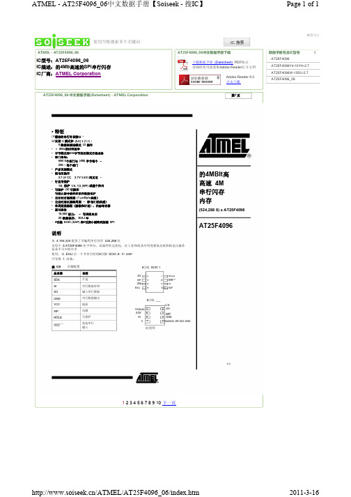
IC型号:AT25F4096_06 IC描述:的4Mb高速的SPI串行闪存 IC厂商:ATMEL Corporation
AT25F4096_06 中文数据手册(Datasheet) - ATMEL Corporation
第2 页
AT25F4096 启用该 (CS) 通过芯片选择引脚 (SI), ,并通过一个 3线接口的串行数据输入输出 (SO), (SCK). 串行数据和串行时钟 1/8, 组成的全部写周期是完全独立的计时 访问。 块写入顶级顶级 1/4, 1/2 WP 顶部或整个记忆体阵列的保护是启用的状态寄存器编程 。单独写使能和写禁止指令 提供额外的数据保护。硬件数据保护是通过提供 HOLD 针,以防止无意中写状态寄存器的尝试。该 +85°C 脚可暂停而不重置串行 序列任何串行通信。
/ATMEL/AT25F4096_06/3.htm
2011-3-16
ATMEL - AT25F4096_06中文数据手册(第4页)【Soiseek - 搜IC】
Page 1 of 1
IC型号大全
使用Firefox(火狐)浏览器提高10倍以上的搜索速度
ATMEL - AT25F4096_06 AT25F4096_06中文数据手册下载 下载数据手册 (Datasheet) PDF格式 请确保使用最新版Adobe Reader 打开文档 Adobe Reader 9.3 点击下载 数据手册包含IC型号 AT25F4096 AT25F4096Y4-10YH-2.7 AT25F4096W-10SU-2.7 AT25F4096_06
图 524,288 框图
8x2
AT25F4096
2454G–SFLSH–5/06
启用该 通过芯片选择引脚,并通过一个3 线接口的串行数据输入输出 串行数据和串行时钟
MR2A16A中文资料

2. All voltages are referenced to VSS. 3. Power dissipation capability depends on package characteristics and use environment.
MR2A16A/D, Rev. 0.1
Freescale Semiconductor
H
X
X
L
X
X
H
H
L
L
H
L
H
L
L
H
H
L
L
L
H
L
L
L
X
L
L
H
L
X
L
H
L
L
X
L
L
L
NOTES: 1. H = high, L = low, X = don’t care 2. Hi-Z = high impedance
Mode
Not selected Output disabled Output disabled Lower byte read Upper byte read Word read Lower byte write Upper byte write Word write
The device also contains protection against external magnetic fields. Precautions should be taken to avoid application of any magnetic field more intense than the maximum field intensity specified in the maximum ratings.
- 1、下载文档前请自行甄别文档内容的完整性,平台不提供额外的编辑、内容补充、找答案等附加服务。
- 2、"仅部分预览"的文档,不可在线预览部分如存在完整性等问题,可反馈申请退款(可完整预览的文档不适用该条件!)。
- 3、如文档侵犯您的权益,请联系客服反馈,我们会尽快为您处理(人工客服工作时间:9:00-18:30)。
Type FCN Surface Mount Film CapacitorsCDE Cornell Dubilier • 1605 E. Rodney French Blvd. • New Bedford, MA 02744 • Phone: (508)996-8561 • Fax: (508)996-3830 • www.cde.comSpecificationsType FCN capacitors are designed for applications requiring a general purpose SMT capacitor with stable temperature and frequency characteristics similar to polyester film capacitors. They are ideal for applications such as EMI noise filtering, power supply input/output filters, audio or signal coupling, and IC power bus bypassing or decoupling. FCN SMT capacitors have a non-inductive stacked metallized PEN film construction which results in a low ESR and excellent high frequency performance.
HighlightsDesigned for reflow solderingWithstands 150% of rated voltage for 60 secondsStacked metallized polyethylene naphthalate (PEN) filmPerforms like polyester capacitorsNonmagnetic and lead-free•••
••
Capacitance Range:Capacitance Tolerance: Voltages:Operating Temperature Range:
IR (at 20 ºC, after 60 seconds):Dissipation Factor (Tanδ):Life Test:
Moisture Resistance:
1000 pF to 1.0 µF (1 kHz at 5 Vrms)±5% (J), ±10% (K) (See Ratings)16, 50, 100, 250 & 400 Vdc16, 50, 100Vdc (<0.012 µF); –55 ºC to +105 ºC100 Vdc (≥ 0.012 µF), 250, 400 Vdc; –40 ºC to +85 ºC
C >0.33 µF: IR = 1000 MΩ•µF Min.C ≤0.33 µF: IR ≥ 3000 MΩ
1.0% Max. (1 kHz at 5 Vrms)1000 h at rated temp. & 125% rated voltage
∆ Capacitance: +1%, –6% max Dissipation Factor: 1.1% max IR: 1000 MΩmin (C>0.33 µF, 300 MΩ•µF min) No significant visual damage
1000 h at 40 ºC and 90 - 95% RH & rated voltage∆ Capacitance: +8/-5% Dissipation Factor: 1.5% max IR: 100 MΩ min (C >0.33 µF, 30 MΩ•µF min) Voltage withstanding: 1.3 times rated voltage, 1 min. No significant damage
Stable Stacked Metallized Film (PEN) Chips for Reflow Soldering Type FCN SMT capacitors are the general purpose line of CDE’s surface mount product offerings. They range in capacitance from .001 µF to 1.0 µF, and they are available in voltage ratings up to 400 Vdc.
Complies with the EU Directive 2002/95/EC requirement restricting the use of Lead (Pb), Mercury (Hg), Cadmium (Cd), Hexavalent chromium (Cr(VI)), PolyBrominated Biphenyls (PBB) and PolyBrominated Diphenyl Ethers (PBDE).
元器件交易网www.cecb2b.comcde.com
Type FCN Surface Mount Film CapacitorsPart Numbering System SpecificationsResistance to Soldering Heat:5 s at max capacitor surface temperature ∆ Capacitance: ±5% max Dissipation Factor: 1.1% max IR: 1000 MΩ min (C >0.33 µF, 300 MΩ•µF min) Voltage withstanding: 1.5 times rated voltage, 1 min. No significant visual damage.
Surface Temperature: 16 V & 50 V & 100 V ≤ 0.01 µF: 240 ºC max 100 V ≥ 0.012 µF, 250 V & 400 V: 230 ºC max
Moisture Resistance:500 h at 85 ºC and 85% RH ∆ Capacitance: ±10% max Dissipation Factor: 2% max IR: 10 MΩ min (C >0.33 µF, 3 MΩ•µF min) Voltage withstanding: 1.3 times rated voltage, 1 min. No significant damage
Withstand Voltage:16 V & 50 V, 100 V ≤ 0.01 µF: 175% ratedvoltage, 5 s100 V ≥ 0.012 µF, 250 V and 400 V: 150% rated voltage, 5 s
FCN1206A102JH2TapeTapePackagingWidthDiameterReel
TypeCase SizeVoltageCapacitanceToleranceCode(mm)[in.(mm)]Quantity
FCN1206C = 16 Vdc102 = 0.001 µFJ = ±5%K1=87 (178)40001913H = 50 Vdc223 = 0.022 µFK = ±10%J1, J2=87 (178)30002416A = 100 Vdc474 = 0.47 µFH1, H2=87 (178)3000
2420E = 250 VdcH3=87 (178)20002820G = 400 VdcG1, G2, G3=87 (178)20003022E1, E2=1213 (330)30003925E3, E4=1213 (330)20003931D1, D2=1213 (330)30006031D3, D4, D5=1213 (330)20006040B, Z=1213 (330)1500U, V, X, Y=1613 (330)1000
S, T=2413 (330)750
元器件交易网www.cecb2b.comType FCN Surface Mount Film CapacitorsCDE Cornell Dubilier • 1605 E. Rodney French Blvd. • New Bedford, MA 02744 • Phone: (508)996-8561 • Fax: (508)996-3830 • www.cde.comOutline Drawing
tLW
T
t = 0.014 ± 0.008 in. (0.35 ±0.2 mm)For 0.001 µF – 0.01 µF, 100 V, t = 0.026 ±0.012 in. (0.62 ± 0.3 mm)Ratings
CapCatalogLWT(µF)Part Numberin (mm)in (mm)in (mm)16 Vdc .12FCN1913C124J-E10.189±0.008 (4.8±0.2)0.130±0.012 (3.3±0.3)0.055±0.008 (1.4±0.2).15FCN1913C154J-E20.189±0.008 (4.8±0.2)0.130±0.012 (3.3±0.3)0.079±0.008 (2.0±0.2).18FCN1913C184J-E20.189±0.008 (4.8±0.2)0.130±0.012 (3.3±0.3)0.079±0.008 (2.0±0.2).22FCN1913C224J-E40.189±0.008 (4.8±0.2)0.130±0.012 (3.3±0.3)0.094±0.008 (2.4±0.2).27FCN2416C274J-D10.236±0.008 (6.0±0.2)0.161±0.012 (4.1±0.3)0.071±0.008 (1.8±0.2).33FCN2416C334J-D20.236±0.008 (6.0±0.2)0.161±0.012 (4.1±0.3)0.079±0.008 (2.0±0.2).39FCN2416C394J-D30.236±0.008 (6.0±0.2)0.161±0.012 (4.1±0.3)0.094±0.008 (2.4±0.2).47FCN2416C474J-D40.236±0.008 (6.0±0.2)0.161±0.012 (4.1±0.3)0.110±0.008 (2.8±0.2)50 Vdc .056FCN1913H563J-E20.189±0.008 (4.8±0.3)0.130±0.012 (3.3±0.3)0.055±0.008 (1.4±0.2)