PCM2702EG4中文资料
PCM2702
PCM2702声卡,加料不加价,全部采用靓声补品电容,不计血本包括主电源在内共计十多只靓声ELNA电容,运放弃用了普通的NE5532,改用更好的AD827或OPA2604,如此高端的配置,使音质达到了更高的层次,是您升级电脑声卡的理想选择,声音超爽啊。
用USB线和电脑USB接口相连,插上电源即可升级你的电脑声卡了,板上没有带耳放功能,线路更简洁,音染更少,音质更纯。
简单说就是一个声音还原的功能。
电源用靓声的LM317高精度稳压,为整板提供高质量的电源。
板上大量采用ELNA补品电容,及多只电容并联应用,保证了声底更纯正,动态更大。
人声厚实,刚柔兼备,极富感性。
良好的动态,低音弹性十足。
高音柔和纤细甜润动人。
中高低音都有很好的表现,总体声音属平衡型。
为了追求音质更加完美,模拟部分用运放缓冲+靓声低噪三极管C2240,D667功率放大的独特形式,舍弃了运放+运放的传统模式,使声音更加真实还原,人声更是运放型无可比拟,更无传统运放的干硬声。
可以驱动耳机或接功放输出。
有运放座,方便您有更好的运放升级用。
本板配AD827或OPA2604。
注:为追求音质更加完美,个别参数如有变动不另行通知,都是发烧级原件,保证更好的品质,让你座享美妙的音质。
板上座子及功能:1)板上装有优质耳机座更加耐用。
可接耳机。
2)二位莲花输出座,接功放。
3)电源输入座。
4)USB输入端子5)电源指示灯。
采用单电源供电(市售成品变压器)电源范围:9V 1A交直流电源或12V1A直流电源。
PCM2702简介:一、PCM2702的性能特点PCM2702拥有很多“同宗兄弟”,它只是其中最早的一款,功能也最简单,不过从音频性能来看,如DNR(动态范围)和SNR(信噪比)指标,性能却是最好的。
BB公司推出的集成USB控制界面的单片数字音频处理器有两大系列,一个以集成DAC为主要特征的PCM27xx系列,另一个是集成DAC和ADC(模数转换器)的PCM29xx系列,具体型号可以从TI公司的网站查阅到。
AP2712

1. 应用范围:1.1该设备用于音频领域内的高精度测量,主要包括:●与计算机相连,可通过编写程序能完成多项自动测试;●模拟测量,用于音频的各种参数指标的测量2. 工作条件:2.1电力供应:单相220V,±10%●电源要求:在100~240V,-10%,+6% AC,50~60Hz范围内正常工作;●环境要求:工作温度5℃~45℃,储存温度-40℃~75℃。
2.3 相对湿度:20-70%。
2.4 仪器运行的持久性:仪器可连续正常运行。
2.5 工作条件及安全性要求符合中国及国际有关标准或规定。
3. 设备的主要技术参数、性能要求和主要配置3.1.硬件主机组成:●双通道独立模拟信号发生器,同时提供BNC,XLR,香蕉接口;含:正弦波、D/A 正弦波、多音等多种信号类型。
●双通道独立模拟信号分析仪,同时提供BNC,XLR,香蕉接口;含下列功能:电平(2通道),电平比率,频率,功率,相位,THD+N失真,噪声,带通幅度,交接干扰。
内置各种高通、低通、带通、AES17滤波器。
●双通道独立数字信号发生器。
格式:SPDIF(同轴/光纤)、AES/EBU、I2S。
●双通道独立数字信号分析仪,格式:SPDIF(同轴/光纤)、AES/EBU、I2S。
FFT频谱分析仪、Multi-tone多音分析仪、谐波(THD, HD)分析仪、MLS扬声器分析仪、数字接口分析仪、数字数据分析仪。
3.2.硬件选件组成:● S2-IMD:内置IMD(互调失真)信号发生器和分析仪● S2-W&F:内置Wow & Flutter 抖摆分析仪,符合IEC/DIN,NAB,JIS和scrape 标准● OPT-2711:内置DOLOBY AC-3 数字信号发生器● S2-BUR内置脉冲、方波、噪音(白噪音/粉红噪音)发生器● FIL-***:内置各种规格之加权滤波器。
A、CCR-468、RCR等。
● AUX-0025:D类功放测试滤波器● PSIA-2722:串行数字信号适配器,可产生和接收I2S信号。
lm2904中文资料
lm2904中文资料LM2439 视频信号输出集成电路LM2453 视频信号输出集成电路LM2577 稳压集成电路LM2595 直流变换集成电路LM270H 自动增益及静噪控制集成电路LM2808N 伴音中频放大、鉴频及功率放大集成电路LM2904 双运算放大集成电路LM3065N 伴音中频放大、鉴频及前置放大集成电路LM3089 调频中频放大集成电路LM311N 电压比较运放集成电路LM317T 三端电源稳压1.5A集成电路LM324 四运算放大集成电路LM324M 四运算放大集成电路LM3361 解调集成电路LM33T 三端电源稳压-26V集成电路LM358 双运算放大集成电路LM358PS-T1 双运算放大集成电路LM3656 伴音中频放大、鉴频及前置放大集成电路LM377 双声道音频功率放大集成电路LM378 双声道音频功率放大集成电路LM380 场扫描输出集成电路LM381 运算放大集成电路LM382 宽带放大集成电路LM384 音频功率放大集成电路LM386 音频功率放大集成电路LM387 宽带放大集成电路LM3875T 音频功率放大集成电路LM3886 音频功率放大集成电路LM3915 发光二极管十位显示驱动集成电路LM399 基准稳压集成电路LM4500A 调频立体声解码集成电路LM4610 音调、音量、平衡调节集成电路LM4765 双声道音频功率放大30W×2集成电路LM741CN 运算放大集成电路LM79052 三端电源稳压-5.2V/1A集成电路LM8915N 显示驱动集成电路LN5241RA89 显示驱动集成电路LP62S512AX-70LLT 存储集成电路LPUVCP-96 端口功能扩展集成电路LR37632 伺服集成电路LR381641 主轴、字符控制集成电路LS0072 变音集成电路LSC4350 屏幕显示控制集成电路LSC4584P2 屏幕显示控制集成电路LT1074 开关电源稳压集成电路LT1109 升压稳压集成电路LTC1147 直流变换集成电路LTC1148 直流变换集成电路LTV1817 光电耦合集成电路LUKS-5140-M2 微处理集成电路LV1011 人工智能处理集成电路LV1100 音频信号处理集成电路LVA501 视频信号处理集成电路LVA521 制式切换集成电路M11B416256A 存储集成电路M1418VVW 微处理集成电路M2063SP 制式转换集成电路M208 系统控制集成电路M24C08 存储集成电路M24C128-WMN6 存储集成电路M27V201-200N6 中文字库集成电路M28F101AVPAD 存储集成电路M3004LAB1 红外遥控信号发射集成电路M32L1632512A 存储集成电路M34300-012SP 微处理集成电路M34300-628SP 微处理集成电路M34300M4-012SP 微处理集成电路M34300N4-011SP 微处理集成电路M34300N4-012SP 微处理集成电路M34300N4-555SP 微处理集成电路M34300N4-567SP 微处理集成电路M34300N4-584SP 微处理集成电路M34300N4-587SP 微处理集成电路M34300N4-628SP 微处理集成电路M34300N4-629SP 微处理集成电路M34300N4-657SP 微处理集成电路M34302M8-612SP 微处理集成电路M37100M8-616SP 微处理集成电路M37102M8-503SP 微处理集成电路M37103M4-750SP 微处理集成电路M37201M6 微处理集成电路M37204M8-852SP 微处理集成电路M37210M2-609SP 微处理集成电路M37210M3-010SP 微处理集成电路M37210M3-550SP 微处理集成电路M37210M3-603SP 微处理集成电路M37210M3-800SP 微处理集成电路M37210M3-901SP 微处理集成电路M37210M3-902SP 微处理集成电路M37210M4-650SP 微处理集成电路M37210M4-688微处理集成电路M37210M4-705SP 微处理集成电路M37210M4-786SP 微处理集成电路M37211M2-604SP 微处理集成电路M37211M2-609SP 微处理集成电路。
PCM2704中文资料

AUDIO DAC WITH USB INTERFACE,ESD damage can range from subtle performance degradation to complete device failure. Precision integrated circuits may be more susceptible to damage because very small parametric changes could cause the device not to meet its published specifications.PACKAGE ORDERING INFORMATION元器件交易网IMPORTANT NOTICETexas Instruments Incorporated and its subsidiaries (TI) reserve the right to make corrections, modifications,enhancements, improvements, and other changes to its products and services at any time and to discontinueany product or service without notice. Customers should obtain the latest relevant information before placingorders and should verify that such information is current and complete. All products are sold subject to TI’s termsand conditions of sale supplied at the time of order acknowledgment.TI warrants performance of its hardware products to the specifications applicable at the time of sale inaccordance with TI’s standard warranty. T esting and other quality control techniques are used to the extent TIdeems necessary to support this warranty. Except where mandated by government requirements, testing of allparameters of each product is not necessarily performed.TI assumes no liability for applications assistance or customer product design. Customers are responsible fortheir products and applications using TI components. T o minimize the risks associated with customer productsand applications, customers should provide adequate design and operating safeguards.TI does not warrant or represent that any license, either express or implied, is granted under any TI patent right,copyright, mask work right, or other TI intellectual property right relating to any combination, machine, or processin which TI products or services are used. Information published by TI regarding third-party products or servicesdoes not constitute a license from TI to use such products or services or a warranty or endorsement thereof.Use of such information may require a license from a third party under the patents or other intellectual propertyof the third party, or a license from TI under the patents or other intellectual property of TI.Reproduction of information in TI data books or data sheets is permissible only if reproduction is withoutalteration and is accompanied by all associated warranties, conditions, limitations, and notices. Reproductionof this information with alteration is an unfair and deceptive business practice. TI is not responsible or liable forsuch altered documentation.Resale of TI products or services with statements different from or beyond the parameters stated by TI for thatproduct or service voids all express and any implied warranties for the associated TI product or service andis an unfair and deceptive business practice. TI is not responsible or liable for any such statements.Following are URLs where you can obtain information on other Texas Instruments products and applicationsolutions:Products ApplicationsAmplifiers Audio /audioData Converters Automotive /automotiveDSP Broadband /broadbandInterface Digital Control /digitalcontrolLogic Military /militaryPower Mgmt Optical Networking /opticalnetworkMicrocontrollers Security /securityTelephony /telephonyVideo & Imaging /videoWireless /wirelessMailing Address:Texas InstrumentsPost Office Box 655303 Dallas, Texas 75265Copyright 2004, Texas Instruments Incorporated。
2732资料

● The ferrite core is a slim EE50-type, leading to a maximum transformer height of 28mm above the PCB
38.1
18.5 25 20 15 15 16.25 16.25 15 20 16.25 20.32 20.32 27
Pitch Power Input (mm) @ 50 kHz (W)
7.5
30
5
40
4
40
5
40
5
40
5
60
5
90
5
190
5
250
5
130
4
40
4
40
5
60
5
90
5
120
5
200
5
● Maximum horizontal dimensions: 51mm x 52mm
Options
● Customized electrical design and pinout
SLOT SMT 100
Series 2642 – Resonant-Type Power Supply Switch-Mode Transformer
SWITCH-MODE TRANSFORMER GUIDE BY TECHNOLOGY
Ferrite
E30/15/7 ETD29X16X10 ETD29X15X10 ETD29X11X10 ETD34X13X11 ETD34X17X11 ETD39X17X13 ER48X18X18 ER54X20X18
RN2702JE中文资料
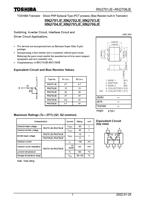
TOSHIBA Transistor Silicon PNP Epitaxial Type (PCT process) (Bias Resistor built-in Transistor)RN2701JE,RN2702JE,RN2703JE RN2704JE,RN2705JE,RN2706JESwitching, Inverter Circuit, Interface Circuit and Driver Circuit Applications.· Two devices are incorporated into an Extreme-Super-Mini (5 pin)package. · Incorporating a bias resistor into a transistor reduces parts count.Reducing the parts count enable the manufacture of ever more compact equipment and save assembly cost. · Complementary to RN1701JE~RN1706JEEquivalent Circuit and Bias Resistor ValuesMaximum Ratings (Ta = 25°C) (Q1, Q2 common)Characteristics SymbolRatingUnitCollector-base voltage V CBO -50 V Collector-emitter voltage RN2701JE~RN2706JE V CEO -50 V RN2701JE~RN2704JE -10 Emitter-base voltage RN2705JE, RN2706JEV EBO -5VCollector currentI C -100 mA Collector power dissipation P C (Note)100 mWJunction temperature T j 150 °CStorage temperature rangeRN2701JE~RN2706JE T stg-55~150°CNote: Total ratingUnit: mmJEDEC― JEITA ― TOSHIBA―Weight: g (typ.)Equivalent Circuit (top view)Type No.R1 (k W ) R2 (k W )RN2701JE 4.7 4.7 RN2702JE 10 10 RN2703JE 22 22 RN2704JE 4747 RN2705JE 2.2 47 RN2706JE 4.747BElectrical Characteristics (Ta = 25°C) (Q1, Q2 common)Characteristics Symbol Test Condition Min Typ. Max UnitI CBO V CB = -50 V, I E = 0 ¾ ¾ -100Collector cut-off currentRN2701JE~2706JEI CEOV CE = -50 V, I B = 0¾ ¾ -500nARN2701JE -0.82 ¾ -1.52RN2702JE-0.38 ¾ -0.71RN2703JE -0.17 ¾ -0.33RN2704JE V EB = -10 V, I C = 0-0.082¾ -0.15RN2705JE -0.078 ¾ -0.145Emitter cut-off currentRN2706JEI EBOV EB = -5 V, I C = 0-0.074¾-0.138mA RN2701JE 30 ¾ ¾RN2702JE 50 ¾ ¾RN2703JE 70 ¾ ¾ RN2704JE 80 ¾ ¾RN2705JE 80 ¾ ¾ DC current gainRN2706JEh FE V CE = -5 V,I C = -10 mA 80 ¾ ¾Collector-emittersaturation voltageRN2701JE~2706JE V CE (sat)I C = -5 mA, I B = -0.25 mA¾ -0.1 -0.3VRN2701JE -1.1 ¾ -2.0 RN2702JE-1.2 ¾ -2.4 RN2703JE -1.3 ¾ -3.0 RN2704JE -1.5 ¾ -5.0 RN2705JE -0.6 ¾ -1.1 Input voltage (ON)RN2706JEV I (ON)V CE = -0.2 V, I C = -5 mA -0.7 ¾ -1.3 V RN2701JE~2704JE -1.0 ¾ -1.5Input voltage (OFF) RN2705JE, 2706JE V I (OFF) V CE = -5 V, I C = -0.1 mA -0.5¾-0.8V Transition frequency RN2701JE~2706JEf TV CE = -10 V, I C = -5 mA¾ 200 ¾ MHz Collector output capacitanceRN2701JE~2706JE C obV CB = -10 V, I E = 0, f = 1 MHz¾ 3 6 pFRN2701JE 3.29 4.7 6.11RN2702JE 7 10 13RN2703JE 15.4 22 28.6RN2704JE32.9 47 61.1RN2705JE 1.54 2.2 2.86Input resistorRN2706JER1¾3.294.7 6.11k WRN2701JE~2704JE0.9 1.0 1.1 RN2705JE 0.0421 0.0468 0.0515Resistor ratioRN2706JER1/R2¾0.09 0.1 0.11Type NameMarking· TOSHIBA is continually working to improve the quality and reliability of its products. Nevertheless, semiconductor devices in general can malfunction or fail due to their inherent electrical sensitivity and vulnerability to physical stress. It is the responsibility of the buyer, when utilizing TOSHIBA products, to comply with the standards of safety in making a safe design for the entire system, and to avoid situations in which a malfunction or failure of such TOSHIBA products could cause loss of human life, bodily injury or damage to property.In developing your designs, please ensure that TOSHIBA products are used within specified operating ranges as set forth in the most recent TOSHIBA products specifications. Also, please keep in mind the precautions and conditions set forth in the “Handling Guide for Semiconductor Devices,” or “TOSHIBA Semiconductor Reliability Handbook” etc.. · The TOSHIBA products listed in this document are intended for usage in general electronics applications (computer, personal equipment, office equipment, measuring equipment, industrial robotics, domestic appliances, etc.). These TOSHIBA products are neither intended nor warranted for usage in equipment that requires extraordinarily high quality and/or reliability or a malfunction or failure of which may cause loss of human life or bodily injury (“Unintended Usage”). Unintended Usage include atomic energy control instruments, airplane or spaceship instruments, transportation instruments, traffic signal instruments, combustion control instruments, medical instruments, all types of safety devices, etc.. Unintended Usage of TOSHIBA products listed in this document shall be made at the customer’s own risk. · The information contained herein is presented only as a guide for the applications of our products. No responsibility is assumed by TOSHIBA CORPORATION for any infringements of intellectual property or other rights of the third parties which may result from its use. No license is granted by implication or otherwise under any intellectual property or other rights of TOSHIBA CORPORATION or others. · The information contained herein is subject to change without notice.000707EAARESTRICTIONS ON PRODUCT USE。
PCM2707EVM-U;中文规格书,Datasheet资料
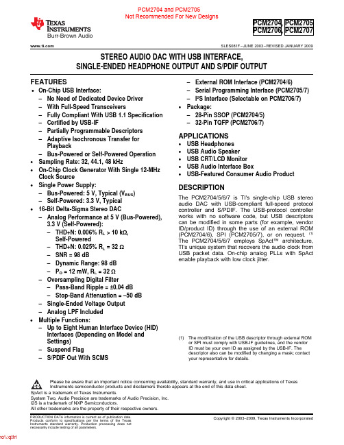
Burr-Brown AudioFEATURESAPPLICATIONSDESCRIPTIONPCM2704,PCM2705PCM2706,PCM2707 SLES081F–JUNE2003–REVISED JANUARY2009 STEREO AUDIO DAC WITH USB INTERFACE,SINGLE-ENDED HEADPHONE OUTPUT AND S/PDIF OUTPUT–External ROM Interface(PCM2704/6)•On-Chip USB Interface:–Serial Programming Interface(PCM2705/7)–No Need of Dedicated Device Driver–I2S Interface(Selectable on PCM2706/7)–With Full-Speed Transceivers•Package:–Fully Compliant With USB1.1Specification–28-Pin SSOP(PCM2704/5)–Certified by USB-IF–32-Pin TQFP(PCM2706/7)–Partially Programmable Descriptors–Adaptive Isochronous Transfer for•USB HeadphonesPlayback•USB Audio Speaker–Bus-Powered or Self-Powered Operation•USB CRT/LCD Monitor•Sampling Rate:32,44.1,48kHz•USB Audio Interface Box•On-Chip Clock Generator With Single12-MHz•USB-Featured Consumer Audio Product Clock Source•Single Power Supply:–Bus-Powered:5V,Typical(V BUS)The PCM2704/5/6/7is TI's single-chip USB stereo –Self-Powered:3.3V,Typical audio DAC with USB-compliant full-speed protocol •16-Bit Delta-Sigma Stereo DAC controller and S/PDIF.The USB-protocol controllerworks with no software code,but USB descriptors –Analog Performance at5V(Bus-Powered),can be modified in some parts(for example,vendor3.3V(Self-Powered):ID/product ID)through the use of an external ROM –THD+N:0.006%R L>10kΩ,(PCM2704/6),SPI(PCM2705/7),or on request.(1) Self-Powered The PCM2704/5/6/7employs SpAct™architecture,TI's unique system that recovers the audio clock from –THD+N:0.025%R L=32ΩUSB packet data.On-chip analog PLLs with SpAct –SNR=98dBenable playback with low clock jitter.–Dynamic Range:98dB–P O=12mW,R L=32Ω–Oversampling Digital Filter–Pass-Band Ripple=±0.04dB–Stop-Band Attenuation=–50dB–Single-Ended Voltage Output–Analog LPF Included•Multiple Functions:–Up to Eight Human Interface Device(HID)Interfaces(Depending on Model and(1)The modification of the USB descriptor through external ROMSettings)or SPI must comply with USB-IF guidelines,and the vendorID must be your own ID as assigned by the USB-IF.The –Suspend Flagdescriptor also can be modified by changing a mask;contact –S/PDIF Out With SCMS your representative for details.Please be aware that an important notice concerning availability,standard warranty,and use in critical applications of TexasInstruments semiconductor products and disclaimers thereto appears at the end of this data sheet.SpAct is a trademark of Texas Instruments.System Two,Audio Precision are trademarks of Audio Precision,Inc.I2S is a trademark of NXP Semiconductors.All other trademarks are the property of their respective owners.PRODUCTION DATA information is current as of publication date.Copyright©2003–2009,Texas Instruments Incorporated Products conform to specifications per the terms of the TexasPCM2704 and PCM2705Not Recommended For New DesignsABSOLUTE MAXIMUM RATINGSRECOMMENDED OPERATING CONDITIONSPCM2704,PCM2705PCM2706,PCM2707SLES081F–JUNE 2003–REVISED JANUARY This integrated circuit can be damaged by ESD.Texas Instruments recommends that all integrated circuits be handled with appropriate precautions.Failure to observe proper handling and installation procedures can cause damage.ESD damage can range from subtle performance degradation to complete device failure.Precision integrated circuits may be more susceptible to damage because very small parametric changes could cause the device not to meet its published specifications.over operating free-air temperature range unless otherwise noted(1)V BUS–0.3V to 6.5V Supply voltageV CCP ,V CCL ,V CCR ,V DD –0.3V to 4V Supply voltage differences V CCP ,V CCL ,V CCR ,V DD±0.1V Ground voltage differences PGND,AGNDL,AGNDR,DGND,ZGND ±0.1V HOST–0.3V to 6.5VDigital input voltageD+,D–,HID0/MS,HID1/MC,HID2/MD,XTI,XTO,DOUT,SSPND,CK,DT,–0.3V to (V DD +0.3)V <4V PSEL,FSEL,TEST,TEST0,TEST1,FUNC0,FUNC1,FUNC2,FUNC3V COM–0.3V to (V CCP +0.3)V <4V Analog input voltageV OUT R –0.3V to (V CCR +0.3)V <4V V OUT L–0.3V to (V CCL +0.3)V <4VInput current (any pins except supplies)±10mA Ambient temperature under bias –40°C to 125°C Storage temperature –55°C to 150°CJunction temperature 150°C Lead temperature (soldering)260°C,5s Package temperature (IR reflow,peak)260°C(1)Stresses beyond those listed under Absolute Maximum Ratings may cause permanent damage to the device.These are stress ratings only,and functional operation of the device at these or any other conditions beyond those indicated under Recommended Operating Conditions is not implied.Exposure to absolute-maximum-rated conditions for extended periods may affect device reliability.over operating free-air temperature rangeMINNOMMAX UNIT V BUS4.3555.25Supply voltage VV CCP ,V CCL ,V CCR ,V DD33.33.6Digital input logic level TTL compatibleDigital input clock frequency 11.9941212.006MHz Analog output load resistance 1632ΩAnalog output load capacitance 100pF Digital output load capacitance 20pF Operating free-air temperature,T A–2585C2Submit Documentation Feedback Copyright ©2003–2009,Texas Instruments IncorporatedPCM2704 and PCM2705Not Recommended For New DesignsELECTRICAL CHARACTERISTICSPCM2704,PCM2705PCM2706,PCM2707 SLES081F–JUNE 2003–REVISED JANUARY 2009all specifications at T A =25°C,V BUS =5V,f S =44.1kHz,f IN =1kHz,16-bit data (unless otherwise noted)PCM2704DB,PCM2705DB,PCM2706PJT,PCM2707PJTPARAMETERTEST CONDITIONSUNITMINTYPMAXDIGITAL INPUT/OUTPUTHost interface Apply USB revision 1.1,full-speed Audio data formatUSB isochronous data formatINPUT LOGIC V IH 23.3V IL –0.30.8Input logic levelVdcV IH (1)2 5.5V IL (1)–0.30.8I IH (2)V IN =3.3V ±10I IL (2)V IN =0V ±10Input logic currentµA I IH V IN =3.3V 65100I ILV IN =0V ±10OUTPUT LOGIC V OH (3)I OH =–2mA2.8V OL (3)I OL =2mA 0.3Output logic levelVdc V OH I OH =–2mA 2.4V OLI OL =2mA0.4CLOCK FREQUENCYInput clock frequency,XTI11.9941212.006MHz f sSampling frequency 32,44.1,48kHz DAC CHARACTERISTICSResolution 16Bits Audio data channel1,2Channel DC ACCURACYGain mismatch,channel-to-channel ±2±8%of FSR Gain error ±2±8%of FSR Bipolar zero error±3±6%of FSR DYNAMIC PERFORMANCE(4)R L >10k Ω,self-powered,0.006%0.01%V OUT =0dBLine(5)Total harmonic R L >10k Ω,bus-powered,THD+N0.012%0.02%distortion +noiseV OUT =0dBR L =32Ω,self-/Headphone0.025%bus-powered,V OUT =0dB THD+N Total harmonic distortion +noise V OUT =–60dB 2%Dynamic range EIAJ,A-weighted 9098dB S/NSignal-to-noise ratio EIAJ,A-weighted9098dB Channel separation6070dB(1)HOST(2)D+,D–,HOST,TEST,TEST0,TEST1,DT,PSEL,FSEL,XTI (3)FUNC0,FUNC1,FUNC2(4)f IN =1kHz,using the System Two™Cascade audio measurement system by Audio Precision™in the RMS mode with a 20-kHz LPF and 400-Hz HPF.(5)THD+N performance varies slightly,depending on the effective output load,including dummy load R7,R8in Figure 32.Copyright ©2003–2009,Texas Instruments Incorporated Submit Documentation Feedback 3PCM2704 and PCM2705Not Recommended For New DesignsPCM2704,PCM2705PCM2706,PCM2707SLES081F–JUNE 2003–REVISED JANUARY ELECTRICAL CHARACTERISTICS (continued)all specifications at T A =25°C,V BUS =5V,f S =44.1kHz,f IN =1kHz,16-bit data (unless otherwise noted)PCM2704DB,PCM2705DB,PCM2706PJT,PCM2707PJTPARAMETERTEST CONDITIONSUNITMINTYPMAXANALOG OUTPUTOutput voltage 0.55V CCL ,0.55V CCRVp-p Center voltage 0.5V CCPV Line AC coupling 10k ΩLoad impedanceHeadphoneAC coupling 1632Ω–3dB 140kHz LPF frequency responsef =20kHz–0.1dB DIGITAL FILTER PERFORMANCEPass band 0.454f sHz Stop band 0.546f sHz Pass-band ripple ±0.04dB Stop-band attenuation –50dB Delay time20/f ssPOWER SUPPLY REQUIREMENTSV BUSBus-powered 4.355 5.25Voltage rangeVdcV CCP ,V CCL ,V CCR ,Self-powered 33.3 3.6V DD LineDAC operation2330mA Supply currentHeadphone DAC operation R L =32Ω)3546Line/headphone Suspend mode (6)150190µA LineDAC operation76108mW Power dissipation Headphone DAC operation R L =32Ω)116166(self-powered)Line/headphone Suspend mode (6)495684µW LineDAC operation115158mW Power dissipation Headphone DAC operation R L =32Ω)175242(bus-powered)Line/headphone Suspend mode (6)750998µW Internal power-supply V CCP ,V CCL ,V CCR ,Bus-powered3.2 3.353.5Vdcvoltage (7)V DDTEMPERATURE RANGEOperating temperature–2585°C28-pin SSOP 100(PCM2704/5)θJAThermal resistance°C/W32-pin TQFP 80(PCM2706/7)(6)Under USB suspend state.(7)V DD ,V CCP ,V CCL ,V CCR .These pins work as output pins of internal power supply for bus-powered operation.4Submit Documentation Feedback Copyright ©2003–2009,Texas Instruments IncorporatedPCM2704 and PCM2705Not Recommended For New DesignsPIN ASSIGNMENTSXTO CK DT PSEL DOUT DGND V DD D–D+V BUS ZGND AGNDL V CCL V OUT LPCM2704/PCM2705DB PACKAGE(TOP VIEW)PCM2706/PCM2707PJT PACKAGE (TOP VIEW)V V OUT V OUT V V B U S+–D DG N D U N C 1U N C 2O U TP G N V C C H O S F U N C F U N C H I D 0/M H I D 1/M H I D 2/M P0020-01PCM2704,PCM2705PCM2706,PCM2707 SLES081F–JUNE 2003–REVISED JANUARY 2009Copyright ©2003–2009,Texas Instruments Incorporated Submit Documentation Feedback 5PCM2704 and PCM2705Not Recommended For New DesignsPCM2704,PCM2705PCM2706,PCM2707SLES081F–JUNE 2003–REVISED JANUARY Terminal Functions (PCM2704DB/PCM2705DB)TERMINAL I/O DESCRIPTIONNAME NO.AGNDL 12—Analog ground for headphone amplifier of L-channel AGNDR 17—Analog ground for headphone amplifier of R-channelCK 2OClock output for external ROM (PCM2704).Must be left open (PCM2705).D+9I/O USB differential input/output plus (1)D–8I/O USB differential input/output minus(1)DGND 6—Digital ground DOUT 5O S/PDIF outputDT 3I/O Data input/output for external ROM (PCM 2704).Must be left open with pullup resistor (PCM2705).(1)HID0/MS 22I HID key state input (mute),active HIGH (PCM2704).MS input (PCM2705).(2)HID1/MC 23I HID key state input (volume up),active HIGH (PCM2704).MC input (PCM2705).(2)HID2/MD 24I HID key state input (volume down),active HIGH (PCM2704).MD input (PCM2705).(2)HOST 21I Host detection during self-powered operation (connect to V BUS ).Max power select during bus-powered operation (LOW:100mA,HIGH:500mA).(3)PGND 19—Analog ground for DAC,OSC,and PLLPSEL 4I Power source select (LOW:self-power,HIGH:bus-power)(1)SSPND 27O Suspend flag,active LOW (LOW:suspend,HIGH:operational)TEST026I Test pin.Must be set HIGH (1)TEST125I Test pin.Must be set HIGH(1)V BUS 10—Connect to USB power (V BUS )for bus-powered operation.Connect to V DD for self-powered operation.V CCL 13—Analog power supply for headphone amplifier of L-channel (4)V CCP 20—Analog power supply for DAC,OSC,and PLL(4)V CCR 16—Analog power supply for headphone amplifier of R-channel (4)V COM 18—Common voltage for DAC (V CCP /2).Connect decoupling capacitor to PGND.V DD 7—Digital power supply(4)V OUT L 14O DAC analog output for L-channel V OUT R 15O DAC analog output for R-channel XTI 28I Crystal oscillator input(1)XTO 1O Crystal oscillator output ZGND 11—Ground for internal regulator(1)LV-TTL level(2)LV-TTL level with internal pulldown (3)LV-TTL level,5-V tolerant(4)Connect decoupling capacitor to GND.Supply 3.3V for self-powered applications.6Submit Documentation Feedback Copyright ©2003–2009,Texas Instruments IncorporatedPCM2704 and PCM2705Not Recommended For New DesignsPCM2704,PCM2705PCM2706,PCM2707 SLES081F–JUNE 2003–REVISED JANUARY 2009Terminal Functions (PCM2706PJT/PCM2707PJT)TERMINAL I/O DESCRIPTIONNAME NO.AGNDL 26—Analog ground for headphone amplifier of L-channel AGNDR 31—Analog ground for headphone amplifier of R-channelCK 14OClock output for external ROM (PCM2706).Must be left open (PCM2707).D+23I/O USB differential input/output plus (1)D–22I/O USB differential input/output minus(1)DGND 20—Digital groundDOUT 17O S/PDIF output/I 2S™data outputDT 15I/O Data input/output for external ROM (PCM2706).Must be left open with pullup resistor (PCM2707).(1)FSEL 9IFunction select (LOW:I 2S DATA output,HIGH:S/PDIF output)(1)FUNC05I/O HID key state input (next track),active HIGH (FSEL =1).I 2S LR clock output (FSEL =0).(2)FUNC119I/O HID key state input (previous track),active HIGH (FSEL =1).I 2S bit clock output (FSEL =0).(2)FUNC218I/O HID key state input (stop),active HIGH (FSEL =1).I 2S system clock output (FSEL =0).(2)FUNC34I HID key state input (play/pause),active HIGH (FSEL =1).I 2S data input (FSEL =0).(2)HID0/MS 6I HID key state input (mute),active HIGH (PCM2706).MS input (PCM2707)(2)HID1/MC 7I HID key state input (volume up),active HIGH (PCM2706).MC input (PCM2707)(2)HID2/MD 8I HID key state input (volume down),active HIGH (PCM2706).MD input (PCM2707)(2)HOST 3I Host detection during self-powered operation (connect to V BUS ).Max power select during bus-powered operation.(LOW:100mA,HIGH:500mA).(3)PGND 1—Analog ground for DAC,OSC,and PLLPSEL 16I Power source select (LOW:self-power,HIGH:bus-power)(1)SSPND 11O Suspend flag,active LOW (LOW:suspend,HIGH:operational)TEST 10I Test pin.Must be set HIGH(1)V BUS 24—Connect to USB power (V BUS )for bus-powered operation.Connect to V DD for self-powered operation.V CCL 27—Analog power supply for headphone amplifier of L-channel (4)V CCP 2—Analog power supply for DAC,OSC,and PLL(4)V CCR 30—Analog power supply for headphone amplifier of R-channel (4)V COM 32—Common voltage for DAC (V CCP /2).Connect decoupling capacitor to PGND.V DD 21—Digital power supply(4)V OUT L 28O DAC analog output for L-channel V OUT R 29O DAC analog output for R-channel XTI 12I Crystal oscillator input(1)XTO 13O Crystal oscillator output ZGND 25—Ground for internal regulator(1)LV-TTL level(2)LV-TTL level with internal pulldown (3)LV-TTL level,5-V tolerant(4)Connect decoupling capacitor to GND.Supply 3.3V for self-powered applications.Copyright ©2003–2009,Texas Instruments Incorporated Submit Documentation Feedback 7PCM2704 and PCM2705Not Recommended For New DesignsSSPNDV V V V ZGNDDGNDAGNDRAGNDLPGNDV COM V OUT LXTI XTO12 MHz V BUSD+D–DT HOSTHID0/MS HID1/MC HID2/MDCK V OUT RDOUT PSEL TEST0TEST1B0054-01PCM2704,PCM2705PCM2706,PCM2707SLES081F–JUNE 2003–REVISED JANUARY BLOCK DIAGRAM (PCM2704DB/PCM2705DB)(1)Applies to PCM2704DB (2)Applies to PCM2705DB8Submit Documentation Feedback Copyright ©2003–2009,Texas Instruments IncorporatedPCM2704 and PCM2705Not Recommended For New DesignsSSPNDVV V V ZGNDDGNDAGNDRAGNDLPGNDV COM V OUT LXTI XTO12 MHz V BUSD+D–DT HOSTHID0/MS HID1/MC HID2/MDCK V OUT RFUNC1DOUTFUNC3PSEL TESTFUNC2FUNC0FSEL B0055-01PCM2704,PCM2705PCM2706,PCM2707 SLES081F–JUNE 2003–REVISED JANUARY 2009BLOCK DIAGRAM (PCM2706PJT/PCM2707PJT)(1)Applies to PCM2706PJT (2)Applies to PCM2707PJTCopyright ©2003–2009,Texas Instruments Incorporated Submit Documentation Feedback 9PCM2704 and PCM2705Not Recommended For New DesignsTYPICAL PERFORMANCE CURVES OF INTERNAL FILTERDAC Digital Interpolation Filter Frequency Responsef – Frequency [× f S ]−140−120−100−80−60−40−20001234A m p l i t u d e – dBG001f – Frequency [× f S ]−0.05−0.04−0.03−0.02−0.010.000.010.020.030.040.050.00.10.20.30.40.5A m p l i t u d e – dBG002DAC Analog Low-Pass Filter Frequency Response−2.0−1.5−1.0−0.50.0f – Frequency – kHzA m p l i t u d e – d B0.011101000.1G003−80−60−40−20f – Frequency – kHzA m p l i t u d e – d B11001k10k10G004PCM2704,PCM2705PCM2706,PCM2707SLES081F–JUNE 2003–REVISED JANUARY All specifications at T A =25°C,V BUS =5V,f S =44.1kHz,f IN =1kHz,16-bit data (unless otherwise noted).AMPLITUDEAMPLITUDEvsvsFREQUENCYFREQUENCYFigure 1.Frequency Response Figure 2.Pass-Band RippleAMPLITUDEAMPLITUDEvsvsFREQUENCYFREQUENCYFigure 3.Pass-Band Characteristics Figure 4.Stop-Band Characteristics10Submit Documentation Feedback Copyright ©2003–2009,Texas Instruments IncorporatedPCM2704 and PCM2705Not Recommended For New Designs分销商库存信息: TIPCM2707EVM-U。
PCM4202资料

ESD damage can range from subtle performance degradation to complete device failure. Precision integrated circuits may be more susceptible to damage because very small parametric changes could cause the device not to meet its published specifications.ABSOLUTE MAXIMUM RATINGSPACKAGING INFORMATIONORDERABLE DEVICESTATUS(1)PACKAGE TYPEPACKAGE DRAWINGPINS PACKAGE QTYPCM4202DB ACTIVE SSOP DB 2848PCM4202DBR ACTIVE SSOP DB 281000PCM4202DBTACTIVESSOPDB28250(1)The marketing status values are defined as follows:ACTIVE:Product device recommended for new designs.LIFEBUY:TI has announced that the device will be discontinued,and a lifetime-buy period is in effect.NRND:Not recommendedfor new designs.Device is in production to support existing customers,but TI does not recommend using this part in a new design.PREVIEW:Device has been announced but is not in production.Samples may or may not be available.OBSOLETE:TI has discontinued the production of the device.PACKAGE OPTION ADDENDUM28-Sep-2004元器件交易网元器件交易网IMPORTANT NOTICETexas Instruments Incorporated and its subsidiaries (TI) reserve the right to make corrections, modifications,enhancements, improvements, and other changes to its products and services at any time and to discontinueany product or service without notice. Customers should obtain the latest relevant information before placingorders and should verify that such information is current and complete. All products are sold subject to TI’s termsand conditions of sale supplied at the time of order acknowledgment.TI warrants performance of its hardware products to the specifications applicable at the time of sale inaccordance with TI’s standard warranty. T esting and other quality control techniques are used to the extent TIdeems necessary to support this warranty. Except where mandated by government requirements, testing of allparameters of each product is not necessarily performed.TI assumes no liability for applications assistance or customer product design. Customers are responsible fortheir products and applications using TI components. T o minimize the risks associated with customer productsand applications, customers should provide adequate design and operating safeguards.TI does not warrant or represent that any license, either express or implied, is granted under any TI patent right,copyright, mask work right, or other TI intellectual property right relating to any combination, machine, or processin which TI products or services are used. Information published by TI regarding third-party products or servicesdoes not constitute a license from TI to use such products or services or a warranty or endorsement thereof.Use of such information may require a license from a third party under the patents or other intellectual propertyof the third party, or a license from TI under the patents or other intellectual property of TI.Reproduction of information in TI data books or data sheets is permissible only if reproduction is withoutalteration and is accompanied by all associated warranties, conditions, limitations, and notices. Reproductionof this information with alteration is an unfair and deceptive business practice. TI is not responsible or liable forsuch altered documentation.Resale of TI products or services with statements different from or beyond the parameters stated by TI for thatproduct or service voids all express and any implied warranties for the associated TI product or service andis an unfair and deceptive business practice. TI is not responsible or liable for any such statements.Following are URLs where you can obtain information on other Texas Instruments products and applicationsolutions:Products ApplicationsAmplifiers Audio /audioData Converters Automotive /automotiveDSP Broadband /broadbandInterface Digital Control /digitalcontrolLogic Military /militaryPower Mgmt Optical Networking /opticalnetworkMicrocontrollers Security /securityTelephony /telephonyVideo & Imaging /videoWireless /wirelessMailing Address:Texas InstrumentsPost Office Box 655303 Dallas, Texas 75265Copyright 2004, Texas Instruments Incorporated。
- 1、下载文档前请自行甄别文档内容的完整性,平台不提供额外的编辑、内容补充、找答案等附加服务。
- 2、"仅部分预览"的文档,不可在线预览部分如存在完整性等问题,可反馈申请退款(可完整预览的文档不适用该条件!)。
- 3、如文档侵犯您的权益,请联系客服反馈,我们会尽快为您处理(人工客服工作时间:9:00-18:30)。
DESCRIPTION
The PCM2702 is a single chip digital-to-analog converter offering two D/A output channels and an integrated USB 1.0 compliant interface controller. The newly developed SpAct™ (Sampling Period Adaptive Controlled Tracking) system recovers a stable, low-jitter clock for internal PLL and DAC operation from the USB interface audio data. The PCM2702 is based upon Texas Instruments Enhanced Multi-level Delta-Sigma Modulator, an 8x oversampling digital interpolation filter, and an analog output low-pass filter. The PCM2702 can accept a 48kHz, 44.1kHz and 32kHz sampling rates, using either 16-bit stereo or monaural audio data. Digital attenuation and soft-mute features are included, and are controlled via USB audio class request.
Patents Pending. SpAct™ is a trademark of Texas Instruments.
Please be aware that an important notice concerning availability, standard warranty, and use in critical applications of Texas Instruments semiconductor products and disclaimers thereto appears at the end of this data sheet. All trademarks are the property of their respective owners.
元器件交易网
PCM2702
PCM 270 2
SBAS142A – MAY 2000 – REVISED NOVEMBER 2007
16-Bit Stereo DIGITAL-TO-ANALOG CONVERTER with Interface
FEATURES
q INTEGRATED USB INTERFACE: Full-Speed Transceiver Supports 12Mbps Data Transfer Fully Compliant with the USB 1.0 Specification Adaptive Mode for Isochronous Transfer Self-Powered Device q ACCEPTS 16-BIT STEREO AND MONO USB AUDIO DATA STREAMS q ANALOG PERFORMANCE (VCC = 5V): Dynamic Range: 100dB (typ at 16-bit) SNR: 105dB (typ) THD+N: 0.002% (typ at 16-bit) Full-Scale Output: 3.1VPP q 8X OVERSAMPLING DIGITAL FILTER: Passband: 0.454fS Stopband: 0.546fS Passband Ripple: ±0.002dB Stopband Attenuation: –82dB q SAMPLING RATE (FS): 32kHz, 44.1kHz, 48kHz q ON-CHIP CLOCK GENERATOR WITH SINGLE 12MHz CLOCK SOURCE q MULTI-FUNCTIONS: Digital Attenuator: 0dB to –64dB, 1dB/step Soft Mute Zero Flag Suspend Flag Playback Flag q DUAL POWER SUPPLIES: +5V for Analog Portion +3.3V for Digital Portion q PACKAGE: SSOP-28
Copyright © 2000-2007, Texas Instruments Incorporated
元器件交易网
ABSOLUTE MAXIMUM RATINGS(1)
Supply Voltage(2) .............................................................................................................. +6.5V Supply Voltage(3) .............................................................................................................. +4.0V Supply Voltage Differences(4) .................................................................................. ±0.1V Supply Voltage Differences(5) .................................................................................. ±0.1V Ground Voltage Differences(6) ................................................................................. ±0.1V Digital Input Voltage(7) ................................................................. –0.3V to VDD + 0.3V Digital Input Voltage(8) ................................................................................ –0.3V to 6.5V Analog Input Voltage ................................................ –0.3V to VCC + 0.3V Input Current (any pins except supplies) ....................................... ±10mA Operating Temperature .................................................. –25°C to +85°C Storage Temperature ..................................................... –55°C to +125°C Junction Temperature .................................................................... +150°C Lead Temperature (soldering, 5s) ................................................. +260°C Package Temperature (IR reflow, peak, 10s) ............................... +235°C NOTES: (1) Stresses above those listed under Absolute Maximum Ratings may cause permanent damage to the device. Exposure to absolute maximum conditions for extended periods may affect device reliability. (2) VCC, VCCL, VCCR, VDDP. (3) VDD, VDDC. (4) Among VCC, VCCL, VCCR, VCCP. (5) Among VDD, VDDC. (6) Among AGND, AGNDL, AGNDR, AGNDP, DGND, DGNDC, and DGNDU. (7) XTI, D+, D–, PLYBCK, SSPND, ZERO, XTO. (8) VBUS, TEST#, TEST2, TEST1, TEST0.
PRODUCTION DATA information is current as of publication date. Products conform to specifications per the terms of Texas Instruments standard warranty. Production processing does not necessarily include testing of all parameters.