NRSG471M100V8X11.5TRF中文资料
NRG ELX1225 2022年7月技术数据:EPoxy封封闭径向NTC热感应器商品介绍说明书

NRGEpoxy sealed radial lead NTC thermistorProduct features• Epoxy sealed radial NTC thermistor • Temperature sensing, quick response time • Bead with ring lug• Wide resistance range:1 k Ω to 470 kΩ•Non-linear change in resistance vs temperaturePb HALOGENHF FREEPackaging information• Bulk, Type 3: 250 parts per poly bag •Bulk, Others: 500 parts per poly bagT able 1. Part numberingNRG a xxy b xxxx Bx c xFamily nameNRGRing lug type1/2/3/ (See mechanicalparameters for details)Resistancexxy= x.x * 10y Ωex: 103 = 1.0 * 103 = 1000 ΩResistance tolerance codeF = ±1%, H = ±3%Beta tolerance codeF = ±1%,G = ±2%,H = ±3%Beta type codeB1 = 25/50, B2 = 25/85Beta value ex: 3465, 4215, etcLead styleDifferent lead dimensionsApplications• Industrial Process Control • Commercial appliances•Battery, supercapacitor and energy storage systems• Uninterruptible power supplies • Consumer appliances •Medical devices•Heating, ventilation and air conditioning, Refrigeration (HVACR)• Food service equipment • IoT• White goods/household appliances •Computer and peripheral productsEnvironmental compliance and general specificationsSee electrical specification table for option details2Technical Data ELX1225Effective July 2022NRGEpoxy sealed radial lead NTC thermistor/electronicsMechanical parameters- mmLug type 1Lug type 2Lug type 3• 26AWG black Insulated lead wire with terminals tinned3Technical Data ELX1225Effective July 2022NRGEpoxy sealed radial lead NTC thermistor /electronics Electrical specificationsPart numberZero power resistance @ 25°C R 25 (kΩ)Ring lug type(Part number code)R 25Tolerance (Part number code)Beta type (Part number code)Beta value (K)Betatolerance (Part number code)Maximum power@ +25°C P max (mW)Dissipationfactor (mW/°C)Thermaltime constant T (second)Operation temperature TL~TU(°C)NRGa103bxxxxBxc 1(1), (2), (3)±1% (F) ,±3% (H)25/85 (B2)3435±2% (G), ±3% (H)50≥ 2.5 (type3) ≥ 3.0 (others)≤ 10 (type3) ≤ 9 (others)-30 to +105NRGa683bxxxxBxc 6.8(1), (2), (3)±1% (F) ,±3% (H)25/85 (B2)3470±2% (G), ±3% (H)50≥ 2.5 (type3) ≥ 3.0 (others)≤ 10 (type3) ≤ 9 (others)-30 to +105NRGa683bxxxxBxc 6.8(1), (2), (3)±1% (F) ,±3% (H)25/85 (B2)3975±2% (G), ±3% (H)50≥ 2.5 (type3) ≥ 3.0 (others)≤ 10 (type3) ≤ 9 (others)-30 to +105NRGa104bxxxxBxc 10(1), (2), (3)±1% (F) ,±3% (H)25/85 (B2)3435±1% (F), ±3% (H)50≥ 2.5 (type3) ≥ 3.0 (others)≤ 10 (type3) ≤ 9 (others)-30 to +105NRGa104bxxxxBxc 10(1), (2), (3)±1% (F) ,±3% (H)25/85 (B2)3975±1% (F), ±3% (H)50≥ 2.5 (type3) ≥ 3.0 (others)≤ 10 (type3) ≤ 9 (others)-30 to +105NRGa203bxxxxBxc 2(1), (2), (3)±1% (F) ,±3% (H)25/85 (B2)3435±1% (F), ±3% (H)50≥ 2.5 (type3) ≥ 3.0 (others)≤ 10 (type3) ≤ 9 (others)-30 to +105NRGa224bxxxxBxc 22(1), (2), (3)±1% (F) ,±3% (H)25/85 (B2)3740±1% (F), ±3% (H)50≥ 2.5 (type3) ≥ 3.0 (others)≤ 10 (type3) ≤ 9 (others)-30 to +105NRGa334bxxxxBxc 33(1), (2), (3)±1% (F) ,±3% (H)25/85 (B2)3975±1% (F), ±3% (H)50≥ 2.5 (type3) ≥ 3.0 (others)≤ 10 (type3) ≤ 9 (others)-30 to +105NRGa474bxxxxBxc 47(1), (2), (3)±1% (F) ,±3% (H)25/85 (B2)4090±1% (F), ±3% (H)50≥ 2.5 (type3) ≥ 3.0 (others)≤ 10 (type3) ≤ 9 (others)-30 to +105NRGa504bxxxxBxc 50(1), (2), (3)±1% (F) ,±3% (H)25/85 (B2)3950±1% (F), ±3% (H)50≥ 2.5 (type3) ≥ 3.0 (others)≤ 10 (type3) ≤ 9 (others)-30 to +105NRGa504bxxxxBxc 50(1), (2), (3)±1% (F) ,±3% (H)25/85 (B2)4050±1% (F), ±3% (H)50≥ 2.5 (type3) ≥ 3.0 (others)≤ 10 (type3) ≤ 9 (others)-30 to +105NRGa105bxxxxBxc 100(1), (2), (3)±1% (F) ,±3% (H)25/85 (B2)4000±1% (F), ±3% (H)50≥ 2.5 (type3) ≥ 3.0 (others)≤ 10 (type3) ≤ 9 (others)-30 to +105NRGa105bxxxxBxc 100(1), (2), (3)±1% (F) ,±3% (H)25/85 (B2)4190±2% (G), ±3% (H)50≥ 2.5 (type3) ≥ 3.0 (others)≤ 10 (type3) ≤ 9 (others)-30 to +105NRGa105bxxxxBxc 100(1), (2), (3)±1% (F) ,±3% (H)25/85 (B2)4360±2% (G), ±3% (H)50≥ 2.5 (type3) ≥ 3.0 (others)≤ 10 (type3) ≤ 9 (others)-30 to +105NRGa475bxxxxBxc 470(1), (2), (3)±1% (F) ,±3% (H)25/85 (B2)4570±2% (G), ±3% (H)50≥ 2.5 (type3) ≥ 3.0 (others)≤ 10 (type3) ≤ 9 (others)-30 to +105NRGa203bxxxxBxc 2(1), (2), (3)±1% (F) ,±3% (H)25/50 (B1)3380±2% (G), ±3% (H)50≥ 2.5 (type3) ≥ 3.0 (others)≤ 10 (type3) ≤ 9 (others)-30 to +105NRGa503bxxxxBxc 5(1), (2), (3)±1% (F) ,±3% (H)25/50 (B1)3420±2% (G), ±3% (H)50≥ 2.5 (type3) ≥ 3.0 (others)≤ 10 (type3) ≤ 9 (others)-30 to +105NRGa503bxxxxBxc 5(1), (2), (3)±1% (F) ,±3% (H)25/50 (B1)3900±2% (G), ±3% (H)50≥ 2.5 (type3) ≥ 3.0 (others)≤ 10 (type3) ≤ 9 (others)-30 to +105NRGa104bxxxxBxc 10(1), (2), (3)±1% (F) ,±3% (H)25/50 (B1)3380±1% (F), ±3% (H)50≥ 2.5 (type3) ≥ 3.0 (others)≤ 10 (type3) ≤ 9 (others)-30 to +105NRGa104bxxxxBxc 10(1), (2), (3)±1% (F) ,±3% (H)25/50 (B1)4000±1% (F), ±3% (H)50≥ 2.5 (type3) ≥ 3.0 (others)≤ 10 (type3) ≤ 9 (others)-30 to +105NRGa104bxxxxBxc 10(1), (2), (3)±1% (F) ,±3% (H)25/50 (B1)3950±1% (F), ±3% (H)50≥ 2.5 (type3) ≥ 3.0 (others)≤ 10 (type3) ≤ 9 (others)-30 to +105NRGa684bxxxxBxc 68(1), (2), (3)±1% (F) ,±3% (H)25/50 (B1)3950±1% (F), ±3% (H)50≥ 2.5 (type3) ≥ 3.0 (others)≤ 10 (type3) ≤ 9 (others)-30 to +105NRGa224bxxxxBxc 22(1), (2), (3)±1% (F) ,±3% (H)25/50 (B1)3700±1% (F), ±3% (H)50≥ 2.5 (type3) ≥ 3.0 (others)≤ 10 (type3) ≤ 9 (others)-30 to +105NRGa474bxxxxBxc 47(1), (2), (3)±1% (F) ,±3% (H)25/50 (B1)3950±1% (F), ±3% (H)50≥ 2.5 (type3) ≥ 3.0 (others)≤ 10 (type3) ≤ 9 (others)-30 to +105NRGa474bxxxxBxc 47(1), (2), (3)±1% (F) ,±3% (H)25/50 (B1)4020±1% (F), ±3% (H)50≥ 2.5 (type3) ≥ 3.0 (others)≤ 10 (type3) ≤ 9 (others)-30 to +105NRGa105bxxxxBxc 100(1), (2), (3)±1% (F) ,±3% (H)25/50 (B1)3950±1% (F), ±3% (H)50≥ 2.5 (type3) ≥ 3.0 (others)≤ 10 (type3) ≤ 9 (others)-30 to +105NRGa105bxxxxBxc 100(1), (2), (3)±1% (F) ,±3% (H)25/50 (B1)4120±2% (G), ±3% (H)50≥ 2.5 (type3) ≥ 3.0 (others)≤ 10 (type3) ≤ 9 (others)-30 to +105NRGa225bxxxxBxc220(1), (2), (3)±1% (F) ,±3% (H)25/50 (B1)4370±2% (G), ±3% (H)50≥ 2.5 (type3) ≥ 3.0 (others)≤ 10 (type3) ≤ 9 (others)-30 to +105a= Enter ring lug type from table above (1, 2, 3) See Mechanical parameters for lug type details b= Enter resistance tolerance code from table above (F = ±1%, H = ±3%)Bx= Enter Beta type code from table above (B1 = 25/50, B2 = 25/85)c= Enter Beta tolerance code from table above (F = ±1%, G = ±2%, H = ±3%)4Technical Data ELX1225Effective July 2022NRGEpoxy sealed radial lead NTC thermistor/electronicsPart number NRG1033435NRG2033435NRG1043435NRG1043975NRG2243740NRG3343975B typeB25/85B25/85B25/85B25/85B25/85B25/85Temperature (°C)Resistance (kΩ)Resistance (kΩ)Resistance (kΩ)Resistance (kΩ)Resistance (kΩ)Resistance(kΩ)-4020.089532539.55751116.42-3919.1491.71304.8337.47541.351045.23-3818.2488.53286.0135.55509.86978.99-3717.3885.46268.4533.74480.37917.34-3616.5682.51252.0632.03452.75859.93-3515.7879.66236.7630.41426.86806.46-3415.0476.9222.4728.88402.6756.62-3314.3374.25209.1127.43379.85710.15-3213.6671.69196.6326.05358.5666.81-3113.0169.22184.9524.76338.48626.37-3012.466.84174.0323.53319.68588.62-2911.8264.54163.8222.36302.02553.36-2811.2662.32154.2521.26285.44520.42-2710.7360.18145.320.22269.86489.64-2610.2358.11136.9119.23255.21460.85-259.7556.12129.0518.3241.44433.93-249.2954.19121.6817.41228.49408.73-238.8552.34114.7816.57216.3385.14-228.4450.54108.315.77204.83363.06-218.0448.81102.2215.02194.03342.36-207.6747.1496.5114.3183.86322.97-197.3145.5391.1513.62174.28304.79-18 6.9643.9786.1212.98165.24287.74-17 6.6442.4781.412.37156.73271.74-16 6.3341.0276.9511.79148.7256.72-15 6.0339.6272.7811.24141.13242.62-14 5.7538.2768.8510.72133.98229.37-13 5.4936.9665.1610.22127.23216.93-12 5.2335.761.689.75120.86205.23-11 4.9934.4958.419.31114.85194.23-10 4.7633.3155.338.88109.16183.88-9 4.5432.1852.428.48103.79174.15-8 4.3331.0849.698.198.71164.98-7 4.1330.0347.117.7393.91156.35-6 3.942944.687.3989.37148.22-5 3.7628.0242.397.0685.07140.56-4 3.5927.0740.23 6.7481133.34-3 3.4226.1538.19 6.4577.15126.54-2 3.2725.2636.27 6.1673.5120.12-1 3.1224.434.45 5.8970.05114.060 2.9823.5732.73 5.6466.78108.341 2.8522.7731.11 5.3963.67102.942 2.722229.58 5.1660.7397.843 2.621.2628.13 4.9457.9493.024 2.4820.5426.76 4.7355.2988.475 2.3719.8425.46 4.5352.7884.176 2.2719.1724.23 4.3450.480.17 2.1718.5223.07 4.1648.1476.258 2.0717.8921.97 3.9845.9972.69 1.9817.2920.93 3.8243.9469.1510 1.8916.7119.95 3.664265.8911 1.8116.1419.01 3.5140.1662.812 1.7315.618.13 3.3738.4159.8713 1.6615.0717.29 3.2336.7457.0914 1.5914.5616.49 3.135.1654.4615 1.5214.0715.74 2.9833.6551.9616 1.4613.615.02 2.8632.2149.5917 1.413.1414.34 2.7430.8547.35181.3412.713.7 2.6429.5445.21T emperature characteristics5Technical Data ELX1225Effective July 2022NRGEpoxy sealed radial lead NTC thermistor /electronics T emperature characteristics, cont.Part number NRG1033435NRG2033435NRG1043435NRG1043975NRG2243740NRG3343975B typeB25/85B25/85B25/85B25/85B25/85B25/85Temperature (°C)Resistance (kΩ)Resistance (kΩ)Resistance (kΩ)Resistance (kΩ)Resistance (kΩ)Resistance(kΩ)191.2812.2713.09 2.5328.343.1920 1.2311.8612.5 2.4327.1241.2721 1.1811.4611.95 2.342639.4422 1.1311.0811.43 2.2524.9337.7123 1.0910.710.93 2.1623.936.0624 1.0410.3510.45 2.0822.9334.49251101022233260.96039.679.57 1.9221.1131.58270.92249.349.16 1.8520.2730.23280.88629.038.77 1.7819.4628.95290.85178.738.4 1.7218.6927.73300.81888.448.05 1.6517.9526.56310.78738.167.71 1.5917.2525.45320.75737.897.39 1.5416.5724.4330.72877.627.09 1.4815.9323.39340.70137.37 6.8 1.4315.3222.43350.67527.13 6.52 1.3814.7321.52360.6502 6.89 6.25 1.3314.1720.64370.6263 6.666 1.2813.6319.81380.6035 6.44 5.76 1.2313.1219.02390.5817 6.23 5.53 1.1912.6318.26400.5608 6.03 5.31 1.1512.1517.54410.5409 5.83 5.1 1.1111.716.84420.5218 5.64 4.9 1.0711.2716.18430.5036 5.45 4.71 1.0410.8615.55440.4861 5.27 4.53110.4614.95450.4693 5.1 4.350.966810.0814.37460.4533 4.94 4.190.93459.7213.82470.438 4.78 4.030.90349.3713.3480.4233 4.62 3.870.87369.0412.79490.4092 4.47 3.730.84498.7212.31500.3957 4.33 3.590.81738.4111.85510.3827 4.19 3.450.79088.1111.41520.3703 4.05 3.330.76537.8310.99530.3584 3.92 3.20.74087.5610.58540.347 3.8 3.090.71737.310.19550.336 3.67 2.970.69467.059.82560.3255 3.56 2.870.6728 6.819.47570.3154 3.44 2.760.6518 6.589.13580.3057 3.34 2.660.6315 6.358.8590.2963 3.23 2.570.6121 6.148.49600.2874 3.13 2.480.5933 5.948.19610.2788 3.03 2.390.5753 5.747.9620.2705 2.93 2.310.5579 5.557.62630.2625 2.84 2.230.5411 5.377.36640.2549 2.75 2.150.525 5.197.1650.2475 2.67 2.080.5094 5.02 6.86660.2404 2.5920.4944 4.86 6.62670.2336 2.51 1.940.4799 4.7 6.4680.227 2.43 1.870.4659 4.55 6.18690.2207 2.35 1.810.4525 4.41 5.97700.2146 2.28 1.750.4395 4.27 5.77710.2087 2.21 1.690.4269 4.13 5.58720.203 2.14 1.630.4148 4.01 5.39730.1976 2.08 1.580.4031 3.88 5.21740.1923 2.02 1.530.3919 3.76 5.04750.1872 1.96 1.480.381 3.64 4.88760.1823 1.9 1.430.3704 3.53 4.72770.1776 1.84 1.380.3603 3.43 4.576Technical Data ELX1225Effective July 2022NRGEpoxy sealed radial lead NTC thermistor/electronicsT emperature characteristics, cont.Part number NRG1033435NRG2033435NRG1043435NRG1043975NRG2243740NRG3343975B typeB25/85B25/85B25/85B25/85B25/85B25/85Temperature (°C)Resistance (kΩ)Resistance (kΩ)Resistance (kΩ)Resistance (kΩ)Resistance (kΩ)Resistance(kΩ)780.173 1.79 1.340.3504 3.32 4.42790.1686 1.73 1.30.3409 3.22 4.28800.1643 1.68 1.260.3318 3.12 4.14810.1602 1.63 1.220.3229 3.03 4.01820.1562 1.59 1.180.3143 2.94 3.89830.1524 1.54 1.140.306 2.85 3.77840.1487 1.49 1.110.298 2.77 3.65850.1451 1.45 1.070.2902 2.69 3.54860.1416 1.41 1.040.2827 2.61 3.43870.1383 1.37 1.010.2754 2.54 3.32880.135 1.330.97640.2684 2.46 3.22890.1319 1.290.9470.2615 2.39 3.12900.1288 1.260.91850.2549 2.32 3.03910.1259 1.220.89110.2486 2.26 2.94920.123 1.190.86470.2424 2.2 2.85930.1202 1.150.83910.2364 2.13 2.77940.1176 1.120.81450.2305 2.07 2.68950.115 1.090.79070.2249 2.02 2.61960.1124 1.060.76780.2194 1.96 2.53970.11 1.030.74560.2141 1.91 2.46980.107610.72420.209 1.86 2.39990.10530.97750.70350.204 1.81 2.321000.10310.95130.68350.1992 1.76 2.251010.10090.9260.66410.1945 1.71 2.191020.09880.90140.64550.19 1.66 2.121030.09680.87770.62740.1856 1.62 2.071040.09480.85470.610.1813 1.58 2.011050.09290.83240.59310.1771 1.54 1.957Technical Data ELX1225Effective July 2022NRGEpoxy sealed radial lead NTC thermistor /electronics T emperature characteristicsPart number NRG1054000NRG1054190NRG1054360NRG2033380NRG1043380NRG1044000B type B25/85B25/85B25/85B25/50B25/50B25/50Temperature (°C)Resistance (kΩ)Resistance (kΩ)Resistance (kΩ)Resistance (kΩ)Resistance (kΩ)Resistance (kΩ)-4031003300360039.8195325-392910.563098.573377.1937.69184.63305.06-382733.692910.373169.1435.71174.87286.45-372568.52734.472974.7933.84165.67269.05-362414.172570.022793.1932.07157.01252.8-352269.932416.232623.4730.41148.84237.61-342135.072272.352464.7828.84141.14223.4-332008.932137.72316.3727.36133.89210.11-321890.92011.652177.5425.96127.04197.67-311780.431893.632047.6324.64120.58186.03-3016771783.071926.0223.39114.48175.13-291580.121679.481812.1622.21108.73164.93-281489.351582.391705.5121.1103.29155.36-271404.261491.361605.6120.0598.15146.4-261324.491405.991511.9819.0593.3138-251249.661325.91424.2218.1188.71130.12-241179.461250.741341.9317.2284.38122.73-231113.571180.21264.7416.3880.28115.8-221051.71113.951192.3315.5876.39109.29-21993.61051.741124.3814.8372.72103.18-20939.01993.291060.5914.1169.2597.44-19887.7938.351000.713.4465.9692.04-18839.47886.71944.4412.862.8486.98-17794.11838.15891.612.1959.8882.21-16751.44792.48841.9311.6257.0977.74-15711.28749.5795.2511.0754.4373.52-14673.48709.06751.3610.5651.9269.56-13637.88670.98710.0810.0749.5365.83-12604.36635.13671.259.647.2762.32-11572.77601.36634.79.1645.1259.01-10542.99569.54600.318.7443.0855.9-9514.92539.56567.938.3541.1552.96-8488.45511.29537.447.9739.3150.2-7463.47484.63508.717.6137.5647.59-6439.9459.49481.657.2735.945.13-5417.65435.77456.14 6.9534.3342.81-4396.65413.38432.1 6.6432.8340.62-3376.81392.25409.42 6.3531.438.56-2358.06372.29388.04 6.0730.0536.61-1340.35353.45367.87 5.8128.7634.770323.6335.65348.83 5.5627.5333.031307.76318.82330.86 5.3226.3631.382292.78302.92313.9 5.0925.2529.833278.61287.88297.88 4.8824.1928.364265.2273.67282.74 4.6723.1826.975252.5260.22268.45 4.4822.2225.666240.48247.49254.93 4.2921.324.427229.09235.44242.16 4.1120.4323.248218.3224.04230.09 3.9419.5922.139208.07213.25218.66 3.7818.821.0710198.37203.02207.86 3.6318.0420.0711189.18193.33197.64 3.4817.3219.1312180.46184.15187.96 3.3416.6318.2313172.19175.45178.81 3.2115.9717.3814164.33167.2170.13 3.0815.3416.5715156.88159.38161.92 2.9614.7315.8116149.81151.96154.14 2.8414.1615.0817143.08144.92146.77 2.7313.6114.418136.7138.24139.78 2.6213.0913.748Technical Data ELX1225Effective July 2022NRGEpoxy sealed radial lead NTC thermistor/electronicsT emperature characteristics, cont.Part number NRG1054000NRG1054190NRG1054360NRG2033380NRG1043380NRG1044000B type B25/85B25/85B25/85B25/50B25/50B25/50Temperature (°C)Resistance (kΩ)Resistance (kΩ)Resistance (kΩ)Resistance (kΩ)Resistance (kΩ)Resistance (kΩ)19130.63131.9133.16 2.5212.5813.1220124.87125.87126.88 2.4212.112.5321119.38120.16120.93 2.3311.6511.9722114.17114.73115.28 2.2411.2111.4423109.21109.57109.92 2.1610.7910.9424104.49104.66104.83 2.0810.3810.4625100100100210102695.7395.5795.41 1.939.639.572791.6691.3591.06 1.859.289.152887.7887.3486.92 1.798.948.762984.0983.5382.99 1.728.628.393080.5779.979.26 1.668.318.033177.2176.4575.71 1.68.017.693274.0273.1672.34 1.547.727.373370.9770.0269.13 1.497.457.063468.0667.0466.07 1.447.19 6.773565.2964.263.17 1.39 6.94 6.493662.6461.4960.41 1.34 6.69 6.223760.1258.9157.78 1.29 6.46 5.973857.7156.4555.27 1.25 6.24 5.723955.4154.152.89 1.2 6.03 5.494053.2151.8650.62 1.16 5.82 5.274151.1149.7348.46 1.12 5.62 5.064249.147.6946.4 1.09 5.43 4.864347.1845.7544.43 1.05 5.25 4.674445.3543.8942.56 1.01 5.08 4.484543.642.1240.780.9809 4.91 4.314641.9240.4339.080.9487 4.75 4.144740.3238.8137.450.9178 4.59 3.984838.7837.2735.910.8881 4.44 3.834937.3235.7934.430.8595 4.3 3.685035.9134.3833.020.832 4.16 3.545134.5733.0431.680.8056 4.03 3.415233.2831.7530.390.7801 3.9 3.285332.0530.5229.160.7556 3.78 3.165430.8629.3427.990.7321 3.66 3.045529.7328.2126.870.7094 3.54 2.935628.6527.1325.810.6875 3.43 2.825727.6126.124.780.6665 3.33 2.725826.6125.1123.810.6462 3.22 2.625925.6524.1722.870.6266 3.12 2.526024.7423.2621.980.6078 3.03 2.436123.8622.3921.130.5896 2.94 2.356223.0121.5620.310.5721 2.85 2.266322.220.7619.530.5553 2.76 2.186421.432018.780.539 2.68 2.116520.6819.2718.060.5233 2.6 2.036619.9618.5717.380.5081 2.52 1.966719.2817.916.720.4935 2.45 1.896818.6117.2516.10.4794 2.38 1.836917.9816.6315.490.4658 2.31 1.777017.3716.0414.920.4526 2.24 1.717116.7815.4714.360.4399 2.18 1.657216.2214.9213.840.4277 2.12 1.597315.6814.413.330.4158 2.06 1.547415.1613.8912.840.40442 1.497514.6513.4112.370.3933 1.94 1.447614.1712.9411.930.3826 1.89 1.397713.7112.511.50.3722 1.84 1.359Technical Data ELX1225Effective July 2022NRGEpoxy sealed radial lead NTC thermistor /electronics T emperature characteristics, cont.Part number NRG1054000NRG1054190NRG1054360NRG2033380NRG1043380NRG1044000B type B25/85B25/85B25/85B25/50B25/50B25/50Temperature (°C)Resistance (kΩ)Resistance (kΩ)Resistance (kΩ)Resistance (kΩ)Resistance (kΩ)Resistance (kΩ)7813.2612.0711.090.3622 1.79 1.37912.8311.6610.690.3526 1.74 1.268012.4211.2610.310.3432 1.69 1.228112.0210.889.950.3342 1.64 1.188211.6310.519.60.3254 1.6 1.148311.2610.169.260.3169 1.56 1.118410.919.828.940.3087 1.51 1.078510.579.58.630.3008 1.47 1.048610.239.188.330.2931 1.44 1.01879.928.888.050.2856 1.40.9746889.618.597.770.2784 1.360.9445899.318.317.510.2714 1.330.9156909.038.047.250.2646 1.290.8877918.757.787.010.2581 1.260.8608928.487.53 6.780.2517 1.230.8349938.237.29 6.550.2455 1.190.8098947.987.06 6.330.2396 1.160.7857957.74 6.84 6.120.2338 1.140.7624967.51 6.62 5.920.2281 1.110.7399977.29 6.42 5.730.2227 1.080.7182987.07 6.22 5.540.2174 1.050.697299 6.87 6.02 5.360.2123 1.030.677100 6.67 5.84 5.190.207310.6575101 6.47 5.66 5.020.20240.9770.6386102 6.29 5.48 4.860.19770.95330.6204103 6.1 5.32 4.710.19320.93030.6027104 5.93 5.16 4.560.18870.90790.5857105 5.765 4.420.18440.88630.569310Technical Data ELX1225Effective July 2022NRGEpoxy sealed radial lead NTC thermistor/electronicsT emperature characteristicsPart number NRG1043950NRG2243700NRG1053950NRG1054120NRG2254370B typeB25/50B25/50B25/50B25/50B25/50Temperature (°C)Resistance (kΩ)Resistance (kΩ)Resistance (kΩ)Resistance (kΩ)Resistance(kΩ)-403252056.32300032508728.94-39304.831932.462819.843053.328171.87-38286.011816.682651.42869.427652.85-37268.461708.422493.872697.437169.11-36252.071607.152346.482536.526718.12-35236.771512.42208.542385.946297.51-34222.481423.72079.412244.975905.11-33209.121340.651958.462112.965538.92-32196.641262.861845.161989.315197.08-31184.961189.971738.981873.454877.85-30174.041121.661639.441764.864579.66-29163.831057.611546.091663.054301.03-28154.26997.531458.531567.574040.59-27145.31941.171376.3614783797.08-26136.92888.281299.231393.953569.34-25129.06838.621226.811315.063356.26-24121.69791.991158.781240.993156.86-23114.78748.181094.871171.432970.19-22108.3707.021034.81106.072795.39-21102.22668.32978.321044.662631.66-2096.52631.94925.21986.932478.25-1991.16597.72875.25932.662334.46-1886.13565.53828.23881.612199.66-1781.4535.23783.97833.582073.24-1676.96506.7742.3788.391954.64-1572.78479.84703.05745.851843.36-1468.86454.53666.07705.81738.91-1365.16430.69631.22668.081640.85-1261.69408.22598.37632.551548.75-1158.41387.03567.39599.061462.23-1055.33367.05538.17567.51380.93-952.43348.19510.59537.751304.51-849.69330.41484.57509.691232.66-747.12313.62460483.221165.09-644.69297.76436.81458.241101.53-542.4282.79414.89434.671041.71-440.23268.64394.19412.42985.41-338.19255.28374.62391.4932.4-236.27242.64356.11371.56882.49-134.45230.7338.62352.81835.46032.73219.4322.07335.09791.15131.11208.71306.41318.34749.39229.58198.59291.59302.5710.02328.13189.02277.56287.53672.9426.76179.96264.28273.36637.88525.46171.37251.69259.96604.84624.23163.24239.77247.27573.66723.07155.53228.48235.26544.22821.98148.23217.77223.89516.43920.93141.31207.61213.12490.181019.95134.74197.98202.92465.381119.02128.51188.84193.25441.951218.13122.6180.18184.08419.811317.29117171.95175.4398.871416.5111.67164.13167.16379.071515.74106.62156.72159.35360.341615.02101.82149.67151.94342.621714.3497.26142.97144.9325.851813.792.93136.61138.23309.9811Technical Data ELX1225Effective July 2022NRG Epoxy sealed radial lead NTC thermistor /electronics T emperature characteristics, cont.Part number NRG104 3950NRG2243700NRG1053950NRG1054120NRG2254370B type B25/50B25/50B25/50B25/50B25/50Temperature (°C)Resistance (kΩ)Resistance (kΩ)Resistance (kΩ)Resistance (kΩ)Resistance (kΩ)1913.0988.81130.56131.89294.952012.584.89124.81125.87280.722111.9581.17119.35120.16267.242211.4377.63114.14114.73254.462310.9374.26109.19109.57242.362410.4571.05104.48104.66230.88251068100100220269.5765.0995.7395.57209.68279.1662.3391.6691.35199.89288.7759.6987.7987.34190.6298.457.1884.183.52181.79308.0554.7980.5879.89173.42317.7152.5177.2376.44165.48327.3950.3374.0373.14157.93337.0948.2670.9870.01150.7734 6.846.2868.0867.02143.9635 6.5244.465.364.18137.4936 6.2542.662.6561.47131.3437640.8860.1358.88125.4938 5.7639.2457.7156.42119.9339 5.5337.6755.4154.07114.6440 5.3136.1753.2151.83109.6141 5.134.7451.149.69104.8242 4.933.3849.0947.65100.2643 4.7132.0747.1745.7195.9244 4.5330.8245.3443.8591.7945 4.3529.6343.5842.0887.8546 4.1928.4941.940.3884.147 4.0327.440.338.7780.5348 3.8726.3538.7637.2277.1349 3.7325.3637.2935.7473.8850 3.5924.435.8834.3370.7951 3.4523.4834.5332.9867.8452 3.3322.6133.2431.6965.0353 3.221.7732.0130.4662.3454 3.0920.9630.8229.2859.7855 2.9720.1929.6928.1557.3356 2.8719.4528.627.075557 2.7618.7527.5626.0452.7758 2.6618.0726.5625.0550.6559 2.5717.4225.624.148.6160 2.4816.7924.6823.246.6761 2.3916.1923.822.3344.8262 2.3115.6222.9621.543.0463 2.2315.0722.1520.741.3564 2.1514.5421.3719.9439.7365 2.0814.0320.6219.2138.1866213.5419.918.536.767 1.9413.0819.2117.8335.2868 1.8712.6318.5517.1933.9269 1.8112.1917.9116.5732.6270 1.7511.7817.315.9731.3871 1.6911.3816.7115.430.1972 1.631116.1514.8629.0573 1.5810.6315.6114.3327.9674 1.5310.2715.0913.8326.9175 1.489.9314.5813.3425.9176 1.439.614.112.8824.9577 1.389.2913.6412.4324.03Eaton Electronics Division 1000 Eaton Boulevard Cleveland, OH 44122United States /electronics© 2022 Eaton All Rights Reserved Printed in USA Publication No. ELX1225 BU-ELX22085July 2022NRG Epoxy sealed radial lead NTC thermistor Technical Data ELX1225Effective July 2022Life Support Policy: Eaton does not authorize the use of any of its products for use in life support devices or systems without the express written approval of an officer of the Company. Life support systems are devices which support or sustain life, and whose failure to perform, when properly used in accordance with instructions for use provided in the labeling, can be reasonably expected to result in significant injury to the user.Eaton reserves the right, without notice, to change design or construction of any products and to discontinue or limit distribution of any products. Eaton also reserves the right to change or update, without notice, any technical information contained in this bulletin.Eaton is a registered trademark.All other trademarks are property of their respective owners.Follow us on social media to get thelatest product and support information.Manual solder+360 °C, 2.5 seconds maximum by soldering iron, distance between soldering position and coating 10 mm minimum.T emperature characteristics, cont.Part number NRG104 3950NRG2243700NRG1053950NRG1054120NRG2254370B type B25/50B25/50B25/50B25/50B25/50Temperature (°C)Resistance (kΩ)Resistance (kΩ)Resistance (kΩ)Resistance (kΩ)Resistance (kΩ)78 1.348.9813.191223.15791.38.6912.7611.5922.31801.268.4112.3411.221.5811.228.1411.9510.8220.72821.187.8811.5610.4519.97831.147.6311.1910.119.26841.117.3910.849.7618.57851.077.1510.499.4317.91861.04 6.9310.169.1217.28871.01 6.719.848.8216.67880.9762 6.59.548.5316.09890.9467 6.39.248.2515.53900.9183 6.118.957.9814.99910.8909 5.928.687.7214.47920.8644 5.748.417.4813.97930.8389 5.578.167.2413.49940.8143 5.47.91713.04950.7905 5.247.67 6.7812.59960.7675 5.087.44 6.5712.17970.7454 4.937.22 6.3611.76980.724 4.787 6.1611.37990.7033 4.64 6.8 5.9710.991000.6833 4.51 6.6 5.7810.631010.6639 4.37 6.4 5.6110.281020.6453 4.25 6.22 5.439.941030.6272 4.13 6.04 5.279.611040.6098 4.01 5.86 5.119.31050.5929 3.89 5.69 4.959。
GF仪表中文说明
第 5 步:设置有误吗? 在有闪动位的情况下,同时按上、下方向键。 将取消被编辑项的最后的设置内容,并返回到 第 3 步。
第 5 页共 8 页
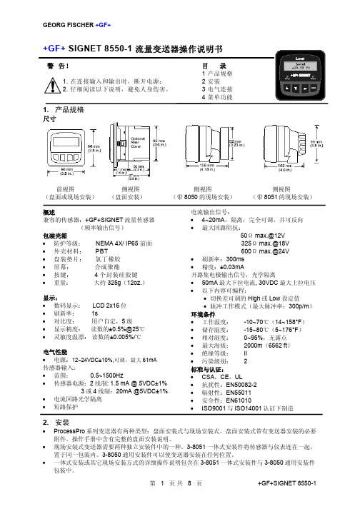
+GF+SIGNET 8550-1
*见辅助电源注意事项
辅助电源注意事项 只有当流量传感器需要的电流超过 1.5mA 时才 要用辅助电源。含有以下 SIGNET 流量传感器 时需要用辅助电源: • 2000 • 2507 • 2540(1999 年 1 月前产品) • 2530 • 2535 • 7002 涡街流量传感器
*见辅助电源注意事项
电气性能
• 电源:12~24VDC±10%,可调,最大 61mA
传感器输入:
• 范围:
0.5~1500Hz
• 传感器电源:2 线制: 1.5 mA @ 5VDC±1%
3 或 4 线制:20mA @5VDC±1%
• 电流回路光学隔离
• 短路保护
电流输出信号:
• 4~20mA,隔离,完全可调,并可反向 • 最大回路阻抗:
3.2 传感器输入连接 接线提示
• 不要将传感器的电缆与 AC 电缆敷设在同一根电缆导管内。电子噪音会干扰传感器信号。 • 将电缆敷设在接地的金属电缆管中有助于防止电子噪音与机械损伤。 • 将电缆入口处密封,以防潮汽的侵害。 • 每个端子只能插入一根导线。如果两根导线接入同一端子,要在外部连好。
对于 515/8510-XX,525,2517,以及任何输出正弦波信号的传 感器,最大电缆长度为 200ft(61m)。
• 工作温度: -10~70℃(14~158°F) • 储存温度: -15~80℃(5~176°F) • 相对湿度: 0~95%,无露点 • 最大海拔: 2000m(6562 ft) • 绝缘等级: II • 污染级别: 2 标准与认证:
Xsens MTi 1-series 数据手册说明书
MTI-3-8A7G6-DKFeatures▪Full-featured AHRS on 12.1 x 12.1 mm module▪Roll/pitch accuracy (dynamic) 1.0 degFigure 1: MTi 1-seriesTable of ContentsT ABLE OF C ONTENTS (2)1GENERAL INFORMATION (3)1.1O RDERING I NFORMATION (3)1.2B LOCK D IAGRAM (3)1.3T YPICAL A PPLICATION (4)1.4P IN C ONFIGURATION (4)1.5P IN MAP (5)1.6P IN D ESCRIPTIONS (6)1.7P ERIPHERAL INTERFACE SELECTION (6)1.7.1I2C (7)1.7.2SPI (7)1.7.3UART half duplex (7)1.7.4UART full duplex with RTS/CTS flow control (8)1.8R ECOMMENDED EXTERNAL COMPONENTS (8)2MTI 1-SERIES ARCHITECTURE (9)2.1MT I 1-SERIES CONFIGURATIONS (9)2.1.1MTi-1 IMU (9)2.1.2MTi-2 VRU (9)2.1.3MTi-3 AHRS (9)2.2S IGNAL PROCESSING PIPELINE (10)2.2.1Strapdown integration (10)2.2.2XKF3TM Sensor Fusion Algorithm (10)2.2.3Frames of reference used in MTi 1-series (11)33D ORIENTATION AND PERFORMANCE SPECIFICATIONS (12)3.13D O RIENTATION SPECIFICATIONS (12)3.2S ENSORS SPECIFICATIONS (12)4SENSOR CALIBRATION (14)5SYSTEM AND ELECTRICAL SPECIFICATIONS (15)5.1I NTERFACE SPECIFICATIONS (15)5.2S YSTEM SPECIFICATIONS (15)5.3E LECTRICAL SPECIFICATIONS (16)5.4A BSOLUTE MAXIMUM RATINGS (16)6MTI 1-SERIES SETTINGS AND OUTPUTS (17)6.1M ESSAGE STRUCTURE (17)6.2O UTPUT SETTINGS (18)6.3MTD ATA2 (19)6.4S YNCHRONIZATION AND TIMING (20)7MAGNETIC INTERFERENCE (21)7.1M AGNETIC F IELD M APPING (21)7.2A CTIVE H EADING S TABILIZATION (AHS) (21)8PACKAGE AND HANDLING (22)8.1P ACKAGE DRAWING (22)8.2P ACKAGING (23)8.3R EFLOW SPECIFICATION (23)9TRADEMARKS AND REVISIONS (24)9.1T RADEMARKS (24)9.2R EVISIONS (24)Figure 2: MTi 1-series module block diagramFigure 3: Typical application Figure 4: Pin assignmentFigure 8: External components (I2C interface) Figure 9: External components (UART interface)2 MTi 1-series architectureThis section discusses the MTi 1-series architecture including the various configurations and the signal processing pipeline.2.1 MTi 1-series configurationsThe MTi 1-series is a fully-tested self-contained module that can 3D output orientation data (Euler angles (roll, pitch, yaw), rotation matrix (DCM) and quaternions), orientation and velocity increments (∆q and ∆v) and sensors data (acceleration, rate of turn, magnetic field). The MTi 1-series module is available as an Inertial Measurement Unit (IMU), Vertical Reference Unit (VRU) and Attitude and Heading Reference System (AHRS). Depending on the product, output options may be limited to sensors data and/or unreferenced yaw.All MTi’s feature a 3D accelerometer/gyroscope combo-sensor, a magnetometer, a high-accuracy crystal and a low-power MCU. The MCU coordinates the synchronization and timing of the various sensors, it applies calibration models (e.g. temperature modules) and output settings and runs the sensor fusion algorithm. The MCU also generates output messages according to the proprietary XBus communication protocol. The messages and the data output are fully configurable, so that the MTi 1-series limits the load, and thus power consumption, on the application processor.2.1.1 MTi-1 IMUThe MTi-1 module is an Inertial Measurement Unit (IMU) that outputs 3D rate of turn, 3D acceleration and 3D magnetic field. The MTi-1 also outputs coning and sculling compensated orientation increments and velocity increments (∆q and ∆v) from its AttitudeEngine TM. Advantages over a gyroscope-accelerometer combo-sensor are the inclusion of synchronized magnetic field data, on-board signal processing and the easy-to-use communication protocol. Moreover, the testing and calibration performed by Xsens result in a robust and reliable sensor module, that can be integrated within a short time frame. The signal processing pipeline and the suite of output options allow access to the highest possible accuracy at any bandwidth, limiting the load on the application processor.2.1.2 MTi-2 VRUThe MTi-2 is a 3D vertical reference unit (VRU). Its orientation algorithm (XKF3TM) outputs 3D orientation data with respect to a gravity referenced frame: drift-free roll, pitch and unreferenced yaw. In addition, it outputs calibrated sensor data: 3D acceleration, 3D rate of turn and 3D earth-magnetic field data. All modules of the MTi 1-series are also capable of outputting data generated by the strapdown integration algorithm (the AttitudeEngine TM outputting orientation and velocity increments ∆q and ∆v). The3D acceleration is also available as so-called free acceleration which has gravity subtracted. Although the yaw is unreferenced, though still superior to gyroscope integration. With the feature Active Heading Stabilization (AHS, see section 7.2) the drift in unreferenced yaw can be limited to 1 deg after 60 minutes, even in magnetically disturbed environments. 2.1.3 MTi-3 AHRSThe MTi-3 supports all features of the MTi-1 and MTi-2, and in addition is a full gyro-enhanced Attitude and Heading Reference System (AHRS). It outputs drift-free roll, pitch and true/magnetic North referenced yaw and sensors data: 3D acceleration, 3D rate of turn, as well as 3D orientation and velocity increments (∆q and ∆v), and 3D earth-magnetic field data. Free acceleration is also available for the MTi-3 AHRS.2.2 Signal processing pipelineThe MTi 1-series is a self-contained module, so all calculations and processes such as sampling, coning and sculling compensation and the Xsens XKF3TM sensor fusion algorithm run on board.2.2.1 Strapdown integrationThe Xsens optimized strapdown algorithm (AttitudeEngine TM) performs high-speed dead-reckoning calculations at 1 kHz allowing accurate capture of high frequency motions. This approach ensures a high bandwidth. Orientation and velocity increments are calculated with full coning and sculling compensation. At an output data rate of up to 100 Hz, no information is lost, yet the output data rate can be configured low enough for systems with limited communication bandwidth. These orientation and velocity increments are suitable for any 3D motion tracking algorithm. Increments are internally time-synchronized with the magnetometer data.2.2.2 XKF3TM Sensor Fusion AlgorithmXKF3 is a sensor fusion algorithm, based on Extended Kalman Filter framework that uses 3D inertial sensor data (orientation and velocity increments) and 3D magnetometer, also known as ‘9D’ to optimally estimate 3D orientation with respect to an Earth fixed frame.XKF3 takes the orientation and velocity increments together with the magnetic field updates and fuses this to produce a stable orientation (roll, pitch and yaw) with respect to the earth fixed frame. The XKF3 sensor fusion algorithm can be processed with filter profiles. These filter profiles contain predefined filter parameter settings suitable for different user application scenarios.The following filter profiles are available:∙General– suitable for most applications.Supported by the MTi-3 module.∙Dynamic– assumes that the motion is highly dynamic. Supported by the MTi-3 module.∙High_mag_dep– heading corrections rely on the magnetic field measured. To be usedwhen magnetic field is homogeneous.Supported by the MTi-3 module.∙Low_mag_dep– heading corrections are less dependent on the magnetic fieldmeasured. Heading is still based onmagnetic field, but more distortions areexpected with less trust being placed onmagnetic measurements. Supported by theMTi-3 module.∙VRU_general– Roll and pitch are thereferenced to the vertical (gravity), yaw isdetermined by stabilized dead-reckoning,referred to as Active Heading Stabilization(AHS) which significantly reduces headingdrift, see also section 7.2. Consider usingVRU_general in environments that have aheavily disturbed magnetic field. TheVRU_general filter profile is the only filterprofile available for the MTi-2-VRU, alsosupported by the MTi-3 modulezxyFigure 10: Default sensor fixed coordinate system for the MTi 1-series moduleIt is straightforward to apply a rotation matrix to the MTi, so that the velocity and orientation increments, free acceleration and the orientation output is output using that coordinate frame. The default reference coordinate system is East-North-Up (ENU) and the MTi 1-series has predefined output options for North-East-Down (NED) and North-West-Up (NWU). Any arbitrary alignment can be entered. These orientation resets have effect on all outputs that are by default outputted with an ENU reference coordinate system.4 Sensor calibrationEach MTi is individually calibrated and tested over its temperature range. The (simplified) sensor model of the gyroscopes, accelerometers and magnetometers can be represented as following:s=K T−1(u−b T)s = sensor data of the gyroscopes, accelerometers and magnetometers in rad/s, m/s2 or a.u. respectivelyK T-1= gain and misalignment matrix (temperature compensated)u = sensor value before calibration (unsigned 16-bit integers from the sensor)b T= bias (temperature compensated)Xsens’ calibration procedure calibrate s for many parameters, including bias (offset), alignment of the sensors with respect to the module PCB and each other and gain (scale factor). All calibration values are temperature dependent and temperature calibrated. The calibration values are stored in non-volatile memory in the MTi.7 Magnetic interferenceMagnetic interference can be a major source of error for the heading accuracy of any Attitude and Heading Reference System (AHRS). As an AHRS uses the magnetic field to reference the dead-reckoned orientation on the horizontal plane with respect to the (magnetic) North, a severe and prolonged distortion in that magnetic field will cause the magnetic reference to be inaccurate. The MTi 1-series module has several ways to cope with these distortions to minimize the effect on the estimated orientation.7.1 Magnetic Field MappingWhen the distortion is deterministic, i.e. when the distortion moves with the MTi, the MTi can be calibrated for this distortion this type of errors are usually referred to as soft and hard iron distortions. The Magnetic Field Mapping procedure compensates for both hard-iron and soft-iron distortions.In short, the magnetic field mapping (calibration) is performed by moving the MTi together with theobject/platform that is causing the distortion. On an external computer (Windows or Linux), the results are processed and the updated magnetic field calibration values are written to the non-volatile memory of the MTi 1-series module. The magnetic field mapping procedure is extensively documented in the Magnetic Field Mapper User Manual (MT0202P), available in the MT Software Suite. 7.2 Active Heading Stabilization (AHS) It is often not possible or desirable to connect the MTi 1-series module to a high-level processor/host system, so that the Magnetic Field Mapping procedure is not an option. Also, when the distortion is non-deterministic the Magnetic Field Mapping procedure does not yield the desired result. For all these situations, the on-board XKF3 sensor fusion algorithm has integrated an algorithm called Active Heading Stabilization (AHS).The AHS algorithm delivers excellent heading tracking accuracy. Heading tracking drift in the MTi 1-series can be as low as 1 deg per hour, while being fully immune to magnetic distortions.AHS is only available in the VRU_general filter profile. This filter profile is the only filter profile in the MTi-2 VRU and one of the 5 available filter profiles in the MTi-3 AHRS.8 Package and handlingNote that this is a mechanical shock (g) sensitive device. Proper handling is required to prevent damage to the part. Note that this is an ESD-sensitive device. Proper handling is required to prevent damage to the part.8.1 Package drawingThe MTi 1-series module is compatible with JEDEC PLCC28 IC-sockets.Figure 11: General tolerances are +/- 0.1 mmFigure 12: Recommended MTi 1-series module footprint8.2 PackagingThe MTi 1-series module is shipped in trays. Trays are available with a MOQ of 20 modules. A full tray contains 152 modules.Figure 13: A tray containing 20 MTi 1-series modules8.3 Reflow specificationThe moisture sensitivity level of the MTi 1-series modules corresponds to JEDEC MSL Level 3, see also: ∙IPC/JEDEC J-STD-020E “Joint Indus try Standard: Moisture/Reflow Sensitivity Classification for non-hermetic Solid State Surface Mount Devices”∙IPC/JEDEC J-STD-033C “Joint Industry Standard: Handling, Packing, Shipping and Use of Moisture/Reflow Sensitive Surface Mount Devices”.The sensor fulfils the lead-free soldering requirements of the above-mentioned IPC/JEDEC standard, i.e. reflow soldering with a peak temperature up to 260°C. Recommended Preheat Area (t s) is 80-100 sec. The minimum height of the solder after reflow shall be at least 50µm. This is required for good mechanical decoupling between the MTi 1-series module and the printed circuit board (PCB) it is mounted on. Assembled PCB’s may NOT be cleaned with ultrasonic cleaning.MTI-3-8A7G6-DK。
RETSCH 产品 说明书

RETSCH 2 X PP 40 40 40/51.5 mm PP 25 32 mm 40 mm
14
12
""
RETSCH
��
PT 100
RETSCH 10 mm 5000
n n
n n
n
n n n n n CE n
RETSCH �
�
1. DIN 51 701 2 AAFCO" "
RETSCH
n PT 100 4
2. 2.5 3
3.
n PK 1000 6
n RT 7
A
A: B: C: D: E:
< 5 mm
2 x 1:7.2
3 x 1:15
*
1 x 1:26
2 x 1:26
3 x 1:26
10 mm
10 mm
10 mm
30 L
��
560 x 1150 x 700 mm
37 kg DR 100
* 10
DIN 45635-31-01-KL3
< 3 mm
LpAeq 63 dBA
PK 1000
50 / 1 2 3
40.411.0001 40.411.0006
42.787.0001 42.787.0003 42.787.0004
22.523.0001 22.523.0002
05.010.0004
RT 6.5 - RT 75
RT 6.5 RT 12.5 3 2.5 L
RT 6.5
12 6.3 mm
8.0 L RT 25RT 37.5RT 50 RT 75
MRF101BN和MRF101AN RF 设备数据手册说明书

MRF101BN MRF101ANMRF101AN MRF101BN1RF Power LDMOS TransistorsHigh Ruggedness N--ChannelEnhancement--Mode Lateral MOSFETsThese devices are designed for use in VHF/UHF communications,VHF TV broadcast and aerospaceapplications as well as industrial,scientific and medical applications.The devices are exceptionally rugged and exhibit high performance up to 250MHz.Typical Performance:V DD =50VdcFrequency (MHz)Signal TypeP out (W)G ps (dB)ηD (%)13.56CW 130CW 27.179.627CW 130CW 24.081.540.68(1)CW 120CW 23.881.550CW 115CW 23.079.581.36CW 130CW 23.280.887.5–108CW 110CW 21.377.1136–174(2,3)CW104CW 21.276.5230(4)Pulse(100μsec,20%Duty Cycle)115Peak21.176.7Load Mismatch/RuggednessFrequency (MHz)Signal TypeVSWR P in (W)Test Voltage Result 40.68CW>65:1at all Phase Angles 0.64Peak (3dB Overdrive)50No Device Degradation 230Pulse(100μsec,20%Duty Cycle)>65:1at all Phase Angles1.8Peak (3dB Overdrive)50No Device Degradation1.Measured in 40.68MHz reference circuit (page 5).2.Measured in 136–174MHz VHF broadband reference circuit (page3.The values shown are the center band performance numbers across the indicated frequency range.4.Measured in 230MHz fixture (page 13).Features ∙Mirror pinout versions (A and B)to simplify use in a push--pull,two--up configuration∙Characterized from 30to 50V ∙Suitable for linear application∙Integrated ESD protection with greater negative gate--source voltage range for improved Class C operation∙Included in NXP product longevity program with assured supply for a minimum of 15years after launchTypical Applications∙Industrial,scientific,medical (ISM)–Laser generation –Plasma etching –Particle accelerators–MRI and other medical applications–Industrial heating,welding and drying systems∙Radio and VHF TV broadcast ∙HF and VHF communications ∙Switch mode power supplies Document Number:MRF101ANRev.0,11/2018Technical Data1.8–250MHz,100W CW,50VWIDEBANDRF POWER LDMOS TRANSISTORSMRF101AN MRF101BNTO--220--3LMRF101BNTO--220--3LMRF101ANGSDDS GNote:Exposed backside of the packageand tab also serves as a source terminal for the transistor.BacksideSS2RF Device Data NXP SemiconductorsMRF101AN MRF101BN Table 1.Maximum RatingsRatingSymbol Value Unit Drain--Source Voltage V DSS –0.5,+133Vdc Gate--Source Voltage V GS –6.0,+10Vdc Operating VoltageV DD 50Vdc Storage Temperature Range T stg –65to +150︒C Case Operating Temperature Range T C –40to +150︒C Operating Junction Temperature Range (1,2)T J –40to +175︒C Total Device Dissipation @T C =25︒C Derate above 25︒CP D1820.91W W/︒CTable 2.Thermal CharacteristicsCharacteristicSymbol Value (2,3)Unit Thermal Resistance,Junction to CaseCW:Case Temperature 77︒C,150W CW,50Vdc,I DQ =100mA,40.68MHz R θJC 1.1︒C/W Thermal Impedance,Junction to CasePulse:Case Temperature 73︒C,113W Peak,100μsec Pulse Width,20%Duty Cycle,50Vdc,I DQ =100mA,230MHzZ θJC0.37︒C/WTable 3.ESD Protection CharacteristicsTest MethodologyClass Human Body Model (per JS--001--2017)1B,passes 1000V Charge Device Model (per JS--002--2014)C3,passes 1200VTable 4.Electrical Characteristics (T A =25︒C unless otherwise noted)CharacteristicSymbolMinTypMaxUnitOff CharacteristicsGate--Source Leakage Current (V GS =5Vdc,V DS =0Vdc)I GSS ——1μAdc Drain--Source Breakdown Voltage (V GS =0Vdc,I D =50mAdc)V (BR)DSS 133——Vdc Zero Gate Voltage Drain Leakage Current (V DS =100Vdc,V GS =0Vdc)I DSS——10μAdcOn CharacteristicsGate Threshold Voltage(V DS =10Vdc,I D =290μAdc)V GS(th) 1.7 2.2 2.7Vdc Gate Quiescent Voltage(V DS =50Vdc,I D =100mAdc)V GS(Q)— 2.5—Vdc Drain--Source On--Voltage (V GS =10Vdc,I D =1Adc)V DS(on)—0.45—Vdc Forward Transconductance (V DS =10Vdc,I D =8.8Adc)g fs—7.1—S1.Continuous use at maximum temperature will affect MTTF.2.MTTF calculator available at /RF/calculators .3.Refer to AN1955,Thermal Measurement Methodology of RF Power Amplifiers.Go to /RF and search for AN1955.(continued)MRF101AN MRF101BN3RF Device DataNXP SemiconductorsTable 4.Electrical Characteristics (T A =25︒C unless otherwise noted)(continued)CharacteristicSymbolMinTypMaxUnitDynamic CharacteristicsReverse Transfer Capacitance(V DS =50Vdc ±30mV(rms)ac @1MHz,V GS =0Vdc)C rss —0.96—pF Output Capacitance(V DS =50Vdc ±30mV(rms)ac @1MHz,V GS =0Vdc)C oss —43.4—pF Input Capacitance(V DS =50Vdc,V GS =0Vdc ±30mV(rms)ac @1MHz)C iss—149—pFTypical Performance —230MHz (In NXP 230MHz Fixture,50ohm system)V DD =50Vdc,I DQ =100mA,P in =0.9W,f =230MHz,100μsec Pulse Width,20%Duty Cycle Common--Source Amplifier Output Power P out —115—W Power Gain G ps —21.1—dB Drain EfficiencyηD—76.7—%Table 5.Load Mismatch/Ruggedness (In NXP 230MHz Fixture,50ohm system)I DQ =100mAFrequency (MHz)Signal TypeVSWR P in (W)Test Voltage,V DDResult230Pulse(100μsec,20%Duty Cycle)>65:1at all Phase Angles1.8Peak (3dB Overdrive)50No Device DegradationTable 6.Ordering InformationDeviceShipping InformationPackageMRF101AN MPQ =250devices (50devices per tube,5tubes per box)TO--220--3L (Pin 1:Gate,Pin 2:Source,Pin 3:Drain)MRF101BNTO--220--3L (Pin 1:Drain,Pin 2:Source,Pin 3:Gate)4RF Device Data NXP SemiconductorsMRF101AN MRF101BNTYPICAL CHARACTERISTICS1100V DS,DRAIN--SOURCE VOLTAGE(VOLTS)Figure1.Capacitance versus Drain--Source Voltage C,CAPACITANCE(pF)1010000.1MRF101AN MRF101BN5RF Device DataNXP Semiconductors40.68MHz COMPACT REFERENCE CIRCUIT (MRF101AN)—0.7"⨯2.0"(1.8cm ⨯5.0cm)Table 7.40.68MHz Performance (In NXP Reference Circuit,50ohm system)V DD =50Vdc,I DQ =100mA,P in =0.50W,CWFrequency (MHz)P out (W)G ps (dB)ηD (%)40.6812023.881.56RF Device Data NXP SemiconductorsMRF101AN MRF101BN 40.68MHz COMPACT REFERENCE CIRCUIT (MRF101AN)—0.7"⨯2.0"(1.8cm ⨯5.0cm)Figure 2.MRF101AN Compact Reference Circuit Component Layout and Assembly Example —40.68MHzFigure 3.MRF101AN Compact Reference CircuitBoardaaa--032274Table 8.MRF101AN Compact Reference Circuit Component Designations and Values —40.68MHzPartDescriptionPart NumberManufacturer B1Short RF Bead 2743019447Fair-Rite C1,C582pF Chip Capacitor GQM2195C2E820GB12D Murata C2,C4200pF Chip Capacitor GQM2195C2A201GB12D Murata C333pF Chip Capacitor GQM2195C2E330GB12D Murata C6,C7,C8,C9,C101000pF Chip Capacitor GRM2165C2A102JA01D Murata C111μF Chip Capacitor GJ821BR71H105KA12L Murata C12,C1310nF Chip Capacitor GRM21BR72A103KA01B Murata C141μF Chip Capacitor C3216X7R2A105K160AA TDK L1150nH Chip Inductor 0805WL151JT ATC L217.5nH,4Turn Inductor GA3095-ACL Coilcraft L3160nH Square Air Core Inductor 2222SQ-161JEC Coilcraft L4110nH Square Air Core Inductor 2222SQ-111JEB Coilcraft Q1RF Power LDMOS Transistor MRF101ANNXP R175Ω,1/4W Chip Resistor SG73P2ATTD75R0F KOA Speer PCBFR40.09",εr =4.8,2oz.CopperD113958MTLMRF101AN MRF101BN7RF Device DataNXP SemiconductorsTYPICAL CHARACTERISTICS —40.68MHz COMPACT REFERENCE CIRCUIT (MRF101AN)V GS ,GATE--SOURCE VOLTAGE (VOLTS)8060P o u t ,O U T P U T P O W E R (W A T T S )40 3.52.51.51100120014020Figure 4.CW Output Power versus Gate--SourceVoltage at a Constant Input PowerP in ,INPUT POWER (WATTS)8060P o u t ,O U T P U T P O W E R (W A T T S )40010012001402040.68101121f (MHz)P1dB (W)P3dB (W)Figure 5.CW Output Power versus Input PowerP out ,OUTPUT POWER (WATTS)Figure 6.Power Gain and Drain Efficiencyversus CW Output PowerG p s ,P O W E R G A I N (d B )ηD ,D R A I N E F F I C I E N C Y (%)25242802090705030302223262729806040201004060801001201400.5230.10.20.30.40.50.60.721201008RF Device Data NXP SemiconductorsMRF101AN MRF101BN40.68MHz COMPACT REFERENCE CIRCUIT(MRF101AN)fMHzZ sourceΩZ loadΩ40.6824.0+j12.614.2–j2.5Z source=Testcircuit impedance as measured fromgate to ground.Z load=Test circuit impedance as measuredfromdrain toground.Figure7.Series Equivalent Source and Load Impedance—40.68MHzZ source Z load50Ω50ΩMRF101AN MRF101BN9RF Device DataNXP Semiconductors136–174MHz COMPACT VHF BROADBAND REFERENCE CIRCUIT (MRF101AN)—0.7"⨯2.0"(1.8cm ⨯5.0cm)Table 9.136–174MHz VHF Broadband Performance (In NXP Reference Circuit,50ohm system)V DD =50Vdc,I DQ =100mA,P in =0.79W,CWFrequency (MHz)P out (W)G ps (dB)ηD (%)13511721.780.015510421.276.517510721.375.4136–174MHz COMPACT VHF BROADBAND REFERENCE CIRCUIT(MRF101AN)—0.7"⨯2.0"(1.8cm⨯5.0cm)Figure8.MRF101AN Compact Reference Circuit Component Layout and Assembly Example—136–174MHzFigure9.MRF101AN Compact Reference Circuit BoardTable10.MRF101AN Compact VHF Broadband Reference Circuit Component Designations and Values—136–174MHz Part Description Part Number ManufacturerB1Short RF Bead2743019447Fair-RiteC139pF Chip Capacitor GQM2195C2E390GB12D MurataC2,C5,C6,C7,C8,C12510pF Chip Capacitor GRM2165C2A511JA01D MurataC368pF Chip Capacitor GQM2195C2E680GB12D MurataC427pF Chip Capacitor GQM2195C2E270GB12D MurataC910pF Chip Capacitor GQM2195C2E100FB12D MurataC111μF Chip Capacitor GJ821BR71H105KA12L MurataC1310nF Chip Capacitor GRM21BR72A103KA01B MurataC141μF Chip Capacitor C3216X7R2A105K160AA TDKL122nH Chip Inductor0805WL220JT ATCL212nH Chip Inductor0805WL120JT ATCL3,L4,L668nH Air Core Inductor1812SMS-68NJLC CoilcraftL512nH,3Turn Inductor GA3094-ALC CoilcraftQ1RF Power LDMOS Transistor MRF101AN NXPR175Ω,1/4W Chip Resistor SG73P2ATTD75R0F KOA SpeerPCB FR40.09",εr=4.8,2oz.Copper D113958MTLTYPICAL CHARACTERISTICS —136–174MHzCOMPACT VHF BROADBAND REFERENCE CIRCUIT (MRF101AN)20150f,FREQUENCY (MHz)26259085807565130120ηD ,D R A I N E F F I C I E N C Y (%)G p s ,P O W E R G A I N (d B )242322211715516016517070110P o u t ,O U T P U T P O W E R (W A T T S )14514017513519100180P in,INPUT POWER (WATTS)0P o u t ,O U T P U T P O W E R (W A T T S )806040200.40.61201000.20.8140 1.027202422807570G p s ,P O W E R G A I N (d B )20406026858025232110012014065605550ηD ,D R A I N E F F I C I E N C Y (%)Figure 10.Power Gain,Drain Efficiency and CW Output Power versus Frequency at a Constant Input PowerFigure 11.CW Output Power versus Input Power and FrequencyP out ,OUTPUT POWER (WATTS)Figure 12.Power Gain and Drain Efficiency versusCW Output Power and Frequency191817454035136–174MHz COMPACT VHF BROADBAND REFERENCE CIRCUIT(MRF101AN)f MHz Z sourceΩZ loadΩ135 6.8+j10.29.5+j5.2145 6.2+j10.29.9+j5.9155 5.3+j10.810.2+j6.2165 4.4+j11.910.0+j5.9175 3.9+j13.48.8+j5.0Z source=Test circuit impedance as measured fromgate to ground.Z load=Test circuit impedance as measured fromdrain to ground.Figure13.Series Equivalent Source and Load Impedance—136–174MHzZ source Z load50Ω50Ω230MHz FIXTURE(MRF101AN)—4.0"⨯5.0"(10.2cm⨯12.7cm)aaa--031939Figure14.MRF101AN Fixture Component Layout—230MHzTable11.MRF101AN Fixture Component Designations and Values—230MHzPart Description Part Number Manufacturer B1Long Ferrite Bead2743021447Fair-RiteC1,C2,C1018pF Chip Capacitor ATC100B180JT500XT ATCC343pF Chip Capacitor ATC100B430JT500XT ATCC4,C131000pF Chip Capacitor ATC800B102JT50XT ATCC50.1μF Chip Capacitor GRM319R72A104KA01D MurataC610nF Chip Capacitor C1210C103J5GACTU KemetC7 2.2μF Chip Capacitor C3225X7R1H225K TDKC847μF,16V Tantalum Capacitor T491D476K016AT KemetC951pF Chip Capacitor ATC100B510JT500XT ATCC1116pF Chip Capacitor ATC100B160JT500XT ATCC12470pF Chip Capacitor ATC800B471JW50XT ATCC140.1μF Chip Capacitor C1812104K1RACTU KemetC15 2.2μF Chip Capacitor C3225X7R2A225K TDKC16 2.2μF Chip Capacitor HMK432B7225KM-T Taiyo YudenC17220μF,100V Electrolytic Capacitor MCGPR100V227M16X26MulticompL139nH Chip Inductor1812SMS-39NJLC CoilcraftL246nH Chip Inductor1010VS-46NME CoilcraftL317.5nH,4Turn Inductor GA3095-ALC CoilcraftR1470Ω,1/4W Chip Resistor CRCW1206470RFKEA VishayPCB Rogers AD255C,0.030",εr=2.55,2oz.Copper D113651MTLTYPICAL CHARACTERISTICS —230MHz FIXTURE,T C =25_C (MRF101AN)0V GS ,GATE--SOURCE VOLTAGE (VOLTS)Figure 15.Output Power versus Gate--SourceVoltage at a Constant Input PowerP o u t ,O U T P U T P O W E R (W A T T S )P E A K755025 1.52 2.531251000.51P in ,INPUT POWER (dBm)PEAK 514943P o u t ,O U T P U T P O W E R (d B m )P E A K4733302127245318230110128f (MHz)P1dB (W)P3dB (W)Figure 16.Output Power versus Input PowerP out ,OUTPUT POWER(WATTS)PEAKFigure 17.Power Gain and Drain Efficiency versus Output Power and Quiescent CurrentG p s ,P O W E R G A I N (d B )ηD ,D R A I N E F F I C I E N C Y (%)3300806040203301080706050403020P out ,OUTPUT POWER (WATTS)PEAKFigure 18.Power Gain and Drain Efficiencyversus Output PowerG p s ,P O W E R G A I N (d B )ηD ,D R A I N E F F I C I E N C Y (%)0P out ,OUTPUT POWER (WATTS)PEAKFigure 19.Power Gain versus Output Powerand Drain--Source Voltage20G p s ,P O W E R G A I N (d B )16145075100182522150451001251503003002441393715230MHz FIXTURE (MRF101AN)f MHz Z sourceΩZ load Ω2302.1+j5.95.5+j3.2Z source =Test circuitimpedance as measured fromgate to ground.Z load=Test circuit impedance asmeasured from drain toground.Figure 20.Series Equivalent Source and Load Impedance —230MHzZ source Z load50Ω50ΩPACKAGE DIMENSIONSPRODUCT DOCUMENTATION,SOFTWARE AND TOOLS Refer to the following resources to aid your design process.Application Notes∙AN1955:Thermal Measurement Methodology of RF Power AmplifiersEngineering Bulletins∙EB212:Using Data Sheet Impedances for RF LDMOS DevicesSoftware∙Electromigration MTTF Calculator∙RF High Power Model∙.s2p FileDevelopment Tools∙Printed Circuit BoardsTo Download Resources Specific to a Given Part Number:1.Go to /RF2.Search by part number3.Click part number link4.Choose the desired resource from the drop down menuREVISION HISTORYThe following table summarizes revisions to this document.Revision Date Description 0Nov.2018∙Initial release of data sheetRF Device DataNXP Semiconductors How to Reach Us:Home Page: Web Support:/support Information in this document is provided solely to enable system and software implementers to use NXP products.There are no express or implied copyright licenses granted hereunder to design or fabricate any integrated circuits based on the information in this document.NXP reserves the right to make changes without further notice to any products herein.NXP makes no warranty,representation,or guarantee regarding the suitability of its products for any particular purpose,nor does NXP assume any liability arising out of the application or use of any product or circuit,and specifically disclaims any and all liability,including without limitation consequential or incidental damages.“Typical”parameters that may be provided in NXP data sheets and/or specifications can and do vary in different applications,and actual performance may vary over time.All operating parameters,including “typicals,”must be validated for each customer application by customer’s technical experts.NXP does not convey any license under its patent rights nor the rights of others.NXP sells products pursuant to standard terms and conditions of sale,which can be found at the following address:/SalesTermsandConditions .NXP and the NXP logo are trademarks of NXP B.V.All other product or service names are the property of their respective owners.E 2018NXP B.V.MRF101BN MRF101AN。
NRLMW222M100V22X35F中文资料

Large Can Aluminum Electrolytic CapacitorsFEATURES• LONG LIFE (105°C, 2000 HOURS)• LOW PROFILE AND HIGH DENSITY DESIGN OPTIONS • EXPANDED CV VALUE RANGE• HIGH RIPPLE CURRENT• CAN-TOP SAFETY VENT • DESIGNED AS INPUT FILTER OF SMPS• STANDARD 10mm (.400") SNAP-IN SPACING NRLMW SeriesSPECIFICATIONSNotice for MountingThe space from the top of the can shall be more than (3mm) from chassis or other construction materials so that safety vent has room to expand in case of emer g en c y.Sleeve Color: Dark BlueCan Top Safety VentInsulation Sleeve and Minus Polarity Marking(4.0mm Leads Available As Option)D+1Max.L ± 26.3 ± 10.810(-)(+)MAXIMUM EX P AN S IONFOR SAFETY VENT Approx. 3.0mmRecommended PC Board Mounting Holes:10 ± .1∅= 2 ± 0.1D ∅ ± 0.5ChassisPC BoardPRECAUTIONSPlease review the notes on correct use, safety and precautions found on pages T10 & T11of NIC’s Electrolytic Capacitor catalog . Operating Temperature Range-40 ~ +105°C -25 ~ +105°C Rated Voltage Range 10 ~ 250Vdc 450Vdc Rated Capacitance Range 180 ~ 68,000µF 56 ~ 470µF Capacitance Tolerance ±20% (M) at 120Hz, +20°CMax. Leakage Current (µA)After 5 minutes (20°C)3 x C(µF)VMax. Tan δat 120Hz/20°CW.V. (Vdc)10162535506380100 ~ 400450Tan δ max.0.550.450.350.300.250.200.170.150.20Surge VoltageW.V. (Vdc)10162535506380100160S.V. (Vdc)132032446379100125200W.V. (Vdc)180200250400450----S.V. (Vdc)220250300450500----Ripple Current Correction Factors Frequency (Hz)50601001205001K 10K ~ 50K --Multiplier at 85°C16 ~ 100Vdc0.930.950.99 1.0 1.05 1.08 1.15--160 ~ 450Vdc0.750.800.95 1.0 1.20 1.25 1.40-Low Temperature Stability (10 to 250Vdc)Temperature (°C)0-25-40------Capacitance Change -5%-10-30%------Impedance Ratio 1.539------Load Life Test 2,000 hours at +105°C Capacitance ChangeWithin ±20% of initial measured valueTan δLess than 200% of specifi ed maximum valueLeakage Current Less than specifi ed maximum value Shelf Life Test 1,000 hours at +105°C(no load)Capacitance ChangeWithin ±20% of initial measured value Tan δLess than 200% of specifi ed maximum valueLeakage Current Less than specifi ed maximum value Surge Voltage TestPer JIS-C-5141 (table #6, #4)Surge voltage applied: 30 seconds "On" and 5.5 minutes no voltage "Off"Capacitance ChangeWithin ±20% of initial measured value Tan δLess than 200% of specifi ed maximum valueLeakage Current Less than specifi ed maximum value Soldering EffectRefer toMIL-STD-202F Method 210ACapacitance ChangeWithin ±10% of initial measured valueTan δLess than specifi ed maximum value Leakage CurrentLess than specifi ed maximum valueRoHSCompliantincludes all homogeneous materials *See Part Number System for DetailsLarge Can Aluminum Electrolytic Capacitors NRLMW SeriesLarge Can Aluminum Electrolytic CapacitorsNRLMW SeriesNRLMW 471 M 250V 30X35 FRoHS compliant Case Size (mm) Voltage Rating Tolerance Code Capacitance Code SeriesPART NUMBER SYSTEM。
WFM200S Wi-Fi Expansion Kit 用户指南说明书
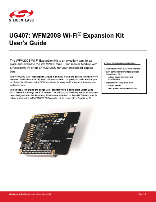
UG407: WFM200S Wi-Fi® Expansion Kit User's GuideThe WFM200S Wi-Fi Expansion Kit is an excellent way to ex-plore and evaluate the WFM200S Wi-Fi Transceiver Module with a Raspberry Pi or an EFM32 MCU for your embedded applica-tion.The WFM200S Wi-Fi Transceiver Module is an easy to use and easy to interface Wi-Fi Network Co-Processor (NCP). Most of the associated complexity of Wi-Fi and the pro-tocol stack is offloaded to the NCP and allows for easy Wi-Fi integration into any em-bedded system.The kit easily integrates and brings Wi-Fi connectivity to a compatible Silicon Labs MCU Starter Kit through the EXP header. The WFM200S Wi-Fi Expansion Kit has also been designed after the Raspberry Pi Hardware Attached on Top (HAT) board specifi-cation, allowing the WFM200S Wi-Fi Expansion Kit to connect to a Raspberry Pi.WFM200S EXPANSION BOARD FEATURES•Selectable SPI or SDIO host interface •EXP connector for interfacing Silicon Labs Starter Kits•Allows board detection andidentification•Raspberry Pi compatible HAT•40-pin header•HAT EEPROM for identificationTable of Contents1. Introduction (3)1.1 Kit Contents (4)2. Hardware Overview (5)2.1 Hardware Layout (5)3. WFM200S Wi-Fi NCP Expansion Kit (6)3.1 Host Interfaces (6)3.2 Power-on and Manual Reset Circuit (7)4. Connectors (8)4.1 EXP Header (9)4.1.1 Pass-through EXP Header (9)4.1.2 EXP Header Pinout (10)4.2 Raspberry Pi Connector (11)4.2.1 Raspberry Pi Connector Pinout (12)4.3 External FEM Connector (13)4.3.1 External FEM Connector Pinout (13)4.4 PTA Connector (14)4.4.1 PTA Connector Pinout (14)4.5 Secondary RF Connector (14)4.6 Power Supply (15)5. Schematics, Assembly Drawings, and BOM (16)6. Kit Revision History (17)6.1 SLEXP8023A Revision History (17)6.2 SLEXP8023C Revision History (17)7. Document Revision History (18)1. IntroductionThis user guide describes the WFM200S Wi-Fi Expansion Kit. The kit connects to either a Silicon Labs EFM32 MCU starter kit (STK), a Silicon Labs EFR32 wireless starter kit (WSTK) or a Raspberry Pi equipped with the 40-pin Raspberry Pi hardware-attached-on-top (HAT) connector. SDIO support is available only with selected hosts.Figures 1.1 and 1.2 shows the kit connected to a Silicon Labs MCU STK through the Expansion Header and a Raspberry Pi, respec-tively.Figure 1.1. WFM200S Wi-Fi Expansion Kit Connected to a Silicon Labs EFM32GG11 MCU STKFigure 1.2. WFM200S Wi-Fi Expansion Kit Connected to a Raspberry Pi Note: Do not connect the kit to both a Silicon Labs MCU STK and a Raspberry Pi at the same time.1.1 Kit ContentsThe WFM200S Wi-Fi Expansion Kit comes in two versions, which differs in what's included in the box:•SLEXP8023A:•BRD8023A WFM200S Wi-Fi EXP Board•8 GB Micro-SD card with software image for Raspberry Pi 2•SLEXP8023C:•BRD8023A WFM200S Wi-Fi EXP Board•8 GB Micro-SD card with software image for Raspberry Pi 2•Raspberry Pi 2 Model B Single-Board Computer•Raspberry Pi Power Supply 5.1 V, 2.5 A2. Hardware Overview2.1 Hardware LayoutThe layout of the WFM200S Wi-Fi Expansion Kit is shown in the figure below.EXP-header for Starter Kits Power source select switchPass-through EXP-header Not mountedRaspberry Pi connectorOn bottom sideCurrent consumptionmeasurement headerNot mountedWFM200S Wi-FiExpansion BoardHost interfaceselect switchSecondary RF outputcoaxial connectorExternal FEM headerNot mountedPTA headerNot mountedReset buttonFigure 2.1. WFM200S Wi-Fi Expansion Kit Hardware LayoutHardware Overview3. WFM200S Wi-Fi NCP Expansion KitThe WFM200S Wi-Fi Transceiver Module is a Wi-Fi Network Co-Processor (NCP) transceiver from Silicon Labs.3.1 Host InterfacesSPI and SDIO are the two available host interfaces (HIF) on the WFM200S Wi-Fi Expansion Kit. A slide switch, whose state is sampled during power-on reset or manually issued reset is used to select the interface. The slide switch must remain in the same position throughout the duration of the session since it also controls HIF selection multiplexer circuits.When the WFM200S Wi-Fi Expansion Kit is connected to an EFM32/EFR32 starter kit through the EXP header, the state of the HIF selection switch can be read (but not controlled) by the kit mcu through a GPIO pin.The WFM200S Wi-Fi Expansion Kit incorporates a set of multiplexer circuits which allows the user to use the same kit for evaluating the WFM200S in both applications requiring SPI or SDIO connectivity to the host. These circuits will normally not be needed in an end-user application since in most cases the interface to use will be fixed.A simplified circuit diagram showing the host interface multiplexer circuits is shown below. The EXP_HEADER9 signal is connected to pin 9 on the EXP header, while the HIF_OEn output enable signal is controlled by the power-on reset circuit (explained later).Figure 3.1. Host Interface Multiplexer Circuit3.2 Power-on and Manual Reset CircuitTo ensure that the state of the host interface selection signal is sampled correctly at the rising edge of the WFM200S RESETn signal, a power-on reset circuit has been added to the WFM200S Wi-Fi Expansion Kit. This circuit achieves this by•Adding a delay of 1ms to the rising edge of the RESETn signal with respect to the rising edge of the power supply•Isolating the host from the WFM200S DAT2/HIF_SEL pin during the rising edge of the RESETn signalThe figure below shows the circuit diagram for the power-on and manual reset circuit. Its functionality is as follows:•NCP_RESETn is the active-low reset signal of the WFM200S. The WFM200S RESETn pin has an internal pull-up of approximately43 kOhms. The on-board reset button is connected to this signal.•HIF_SEL_CTRL is the signal from the HIF selection switch•HIF_OEn is the active-low output enable signal of the HIF multiplexer circuits•WF_DAT2_HIF_SEL is the combined SDIO DAT2 signal and HIF selection signal of the WFM200S•U114 is an open-drain active low output reset monitor which with the installed capacitor connected to the CD pin keeps NCP_RE-SETn tied to ground for about 1 ms after VMCU_NCP has exceeded the threshold voltage of 0.9 V•U115 is a tri-state output buffer with an active low output enable signal connected to NCP_RESETn which pulls the CD pin of U116 low while NCP_RESETn is low•U116 is a push-pull active high output reset monitor which drives HIF_OEn high for 1 ms after the output of U115 is disabled•U109 is a tri-state output buffer with an active high output enable signal which connects the HIF_SEL_CTRL signal to the WF_DAT2_HIF_SEL signal as long as HIF_OEn is highThe NCP_RESETn signal is available on both the EXP header and the Raspberry Pi connector and can be used for issuing a manual reset sequence by pulling it low for at least 1 ms.Note: Reset button is effective when board is not connected to MCU or Raspberry Pi boards. When connected, change of host inter-face is effective after reboot.Figure 3.2. Power-on and Manual Reset Circuit Diagram4. ConnectorsThis chapter gives an overview of the WFM200S Wi-Fi Expansion Kit connectivity and power connections.Pass-through EXP Header(Bottom side)External FEM connector Figure 4.1. WFM200S Wi-Fi Expansion Kit Connector Layout4.1 EXP HeaderOn the left-hand side of the WFM200S Wi-Fi Expansion Kit, a right-angle female 20-pin EXP header is provided to connect to one of Silicon Labs’ supported Starter Kits. The EXP header on the Starter Kits follows a standard which ensures that commonly used periph-erals such as an SPI, a UART, and an I 2C bus, are available on fixed locations on the connector. Additionally, the VMCU, 3V3 and 5 V power rails are also available on the expansion header. For detailed information regarding the pinout to the expansion header on a specific Starter Kit, consult the accompanying user’s guide.The figure below shows how the WFM200S Wi-Fi Transceiver Module is connected to the connector and the peripheral functions that are available.VMCUSPI_MOSI / SDIO_DAT1SPI_MISO / SDIO_DAT0SPI_SCLK / SDIO_CMD SPI_CS / SDIO_CLK SPI_WIRQ / SDIO_DAT3SDIO_DAT2Not Connected (NC)5V3V3GNDGPIO_WUP Not Connected (NC)RESETnHIF_SEL_CTRL Not Connected (NC)Not Connected (NC)Not Connected (NC)BOARD_ID_SDA BOARD_ID_SCL Reserved (Board Identification)WFM200S I/O PinFigure 4.2. Expansion Header4.1.1 Pass-through EXP HeaderThe WFM200S Wi-Fi Expansion Kit features a footprint for a secondary EXP header. All signals from the EXP header, including those that are not connected to any features on the WFM200S Wi-Fi Expansion Kit, are directly tied to the corresponding pins in the footprint,allowing daisy-chaining of additional expansion boards if a connector is soldered in.4.1.2 EXP Header PinoutThe table below shows the pin assignments of the EXP header.Table 4.1. EXP Header Pinout4.2 Raspberry Pi ConnectorOn the bottom side of the WFM200S Wi-Fi Expansion Kit, a dual row, female socket, 0.1" pitch connector is installed to allow the WFM200S Wi-Fi Expansion Kit to act as a Raspberry Pi Hardware Attached on Top (HAT) board.The figure below shows how the WFM200S Wi-Fi Transceiver Module is connected to the connector and the peripheral functions that are available.Reserved (Board Identification)WFM200S I/O PinGNDSDIO_DAT2Not Connected (NC)RESETnGPIO_WIRQNot Connected (NC)RPI_ID_SDGND SPI_SCLKSPI_MISO Not Connected (NC)Not Connected (NC)SPI_WIRQGNDGPIO_WUP GNDRPI_ID_SC Not Connected (NC)SDIO_DAT1SPI_CSSPI_MOSI 3V3SDIO_CLKSDIO_DAT3 Not Connected (NC)GNDNot Connected (NC)Not Connected (NC) Not Connected (NC)3V3GNDSDIO_DAT0SDIO_CMD GNDNot Connected (NC)GPIO_FEM_5GPIO_FEM_6GND5V 5VFigure 4.3. Raspberry Pi Connector4.2.1 Raspberry Pi Connector PinoutThe table below shows the pin assignments of the Raspberry Pi connector, and the port pins and peripheral functions that are available on the WFM200S Wi-Fi Expansion Kit.Table 4.2. Raspberry Pi Connector Pinout4.3 External FEM ConnectorThe WFM200S Wi-Fi Expansion Kit features a 2x5-pin 0.1" pitch connector exposing the WFM200S Wi-Fi Transceiver Module's exter-nal front-end module (FEM) interface, which allows the connection of an external FEM board using a ribbon cable.The WFM200S Wi-Fi Expansion Kit also features a TX/RX activity indicator LED which is connected to the FEM_5 signal. By default, to optimize power consumption, TX/RX activity LED is not enabled. PDS sections PROG_PINS_CFG and FEM_CFG should be updated to enable this functionality.The pinout of the connector is illustrated in the figure below.GNDFEM_PDETFEM_6FEM_5VMCU_NCPFEM_4FEM_3VMCU_NCPFEM_2FEM_1Figure 4.4. External FEM Connector4.3.1 External FEM Connector PinoutThe pin assignment of the external FEM connector on the board is given in the table below.Table 4.3. External FEM Connector Pin Descriptions4.4 PTA ConnectorThe WFM200S' packet transfer arbitration (PTA) interface for managing coexistence in a multi-transceiver application is exposed on a 1x5-pin 0.1" pitch header on the WFM200S Wi-Fi Expansion Kit.The pinout of the connector is illustrated in the figure below.PTA_STATUS / PRIORITY PTA_RF_ACT / REQUESTPTA_FREQ / RHOPTA_TX_CONF / GRANT GNDFigure 4.5. PTA Connector4.4.1 PTA Connector PinoutThe pin assignment of the PTA connector on the board is given in the table below.Table 4.4. PTA Connector Pin Descriptions4.5 Secondary RF ConnectorThe WFM200S' secondary RF output is exposed on the WFM200S Wi-Fi Expansion Kit through a Hirose u.FL coaxial connector.For connecting the secondary RF output to an RF measurement instrument, 50 ohms resistor R641 shall be removed and a u.FL to SMA adapter cable (not included with the kit) can be used. Examples of such adapter cables are the Taoglas CAB.721 (100 mm) or CAB.720 (200 mm) cable assemblies.4.6 Power SupplyThere are two ways to provide power to the kit:•The kit can be connected to, and powered by, a Silicon Labs MCU STK •The kit can be connected to, and powered by, a Raspberry PiNote: Connecting the WFM200S Wi-Fi Expansion Kit to both an EFM32/EFR32 STK and a Raspberry Pi at the same time is not a valid option.When connected to a Silicon Labs MCU STK, the WFM200S Wi-Fi Transceiver Module can either be powered by the VMCU rail present on the EXP header or through an LDO regulator on board the WFM200S Wi-Fi Expansion Kit. If connected to the VMCU rail of the starter kit, the current consumption of the WFM200S Wi-Fi Transceiver Module will be included in the starter kit's on-board Ad-vanced Energy Monitor (AEM) measurements. The LDO regulator draws power from the 5V net, and, hence, the power consumption of the WFM200S Wi-Fi Transceiver Module will not be included in any AEM measurements performed by the MCU STK.A mechanical power switch on the WFM200S Wi-Fi Expansion Kit is used to select between Low Power (AEM) mode and High Power (LDO) mode. When the switch is set to Low Power (AEM) mode, the WFM200S Wi-Fi Transceiver Module is connected to the VMCU net on the Expansion Header. When the switch is set to High Power (LDO) mode, the WFM200S Wi-Fi Transceiver Module is connec-ted to the output of the LDO. For applications requiring high power consumption or when the WFM200S Wi-Fi Expansion Kit is connec-ted to a Raspberry Pi, the power switch must be set to High Power (LDO) mode.A 0.1 ohm current sense resistor accompanied by a 2x2-pin 0.1" unpopulated header is provided to measure the current consumption of the WFM200S Wi-Fi Transceiver Module whenever AEM is not available or when the current consumption exceeds the measure-ment range of AEM.The power topology is illustrated in the figure below.Expansion HeaderRaspberry Pi ConnectorFigure 4.6. WFM200S Wi-Fi Expansion Kit Power TopologySchematics, Assembly Drawings, and BOM 5. Schematics, Assembly Drawings, and BOMSchematics, assembly drawings, and bill of materials (BOM) are available through Simplicity Studio when the kit documentation pack-age has been installed. They are also available from the Silicon Labs website and kit page.6. Kit Revision HistoryThe kit revision can be found printed on the kit packaging label, as outlined in the figure below.SLEXP8023A WFM200S Wi-Fi Expansion Kit194000022401-11-19A01Figure 6.1. Kit Label6.1 SLEXP8023A Revision History6.2 SLEXP8023C Revision History Kit Revision HistoryDocument Revision History 7. Document Revision HistoryRevision 1.02019-11-01•Initial document revision.Simplicity StudioOne-click access to MCU and wireless tools, documentation, software, source code libraries & more. Available for Windows, Mac and Linux!IoT Portfolio /IoTSW/HW/simplicityQuality/qualitySupport and CommunitySilicon Laboratories Inc.400 West Cesar ChavezAustin, TX 78701USADisclaimerSilicon Labs intends to provide customers with the latest, accurate, and in-depth documentation of all peripherals and modules available for system and software implementers using or intending to use the Silicon Labs products. Characterization data, available modules and peripherals, memory sizes and memory addresses refer to each specific device, and "Typical" parameters provided can and do vary in different applications. Application examples described herein are for illustrative purposes only. Silicon Labs reserves the right to make changes without further notice to the product information, specifications, and descriptions herein, and does not give warranties as to the accuracy or completeness of the included information. Without prior notification, Silicon Labs may update product firmware during the manufacturing process for security or reliability reasons. Such changes will not alter the specifications or the performance of the product. Silicon Labs shall have no liability for the consequences of use of the information supplied in this document. This document does not imply or expressly grant any license to design or fabricate any integrated circuits. The products are not designed or authorized to be used within any FDA Class III devices, applications for which FDA premarket approval is required or Life Support Systems without the specific written consent of Silicon Labs. A "Life Support System" is any product or system intended to support or sustain life and/or health, which, if it fails, can be reasonably expected to result in significant personal injury or death. Silicon Labs products are not designed or authorized for military applications. Silicon Labs products shall under no circumstances be used in weapons of mass destruction including (but not limited to) nuclear, biological or chemical weapons, or missiles capable of delivering such weapons. Silicon Labs disclaims all express and implied warranties and shall not be responsible or liable for any injuries or damages related to use of a Silicon Labs product in such unauthorized applications.Trademark InformationSilicon Laboratories Inc.® , Silicon Laboratories®, Silicon Labs®, SiLabs® and the Silicon Labs logo®, Bluegiga®, Bluegiga Logo®, Clock B uilder®, CMEMS®, DSPLL®, EFM®, EFM32®, EFR, Ember®, Energy Micro, Energy Micro logo and combinations thereof, "the world’s most energy friendly microcontrollers", Ember®, EZLink®, EZRadio®, EZRadioPRO®, Gecko®, Gecko OS, Gecko OS Studio, ISOmodem®, Precision32®, ProSLIC®, Simplicity Studio®, SiPHY®, Telegesis, the Telegesis Logo®, USBXpress® , Zentri, the Zentri logo and Zentri DMS, Z-Wave®, and others are trademarks or registered trademarks of Silicon Labs. ARM, CORTEX, Cortex-M3 and THUMB are trademarks or registered trademarks of ARM Holdings. Keil is a registered trademark of ARM Limited. Wi-Fi is a registered trademark of the Wi-Fi Alliance. All other products or brand names mentioned herein are trademarks of their respective。
SD25-471中文资料
Description• Six sizes of shielded drum core inductors with low profiles (as low as 1.0mm) and high power density • Inductance range from .47uH to 1000uH• Current range from 6.00 to 0.088 Amps• Ferrite shielded, low EMIApplications• Digital cameras, CD players, cellular phones, and PDAs • PCMCIA cards• GPS systemsEnvironmental Data• Storage temperature range:-40C to +125C• Operating ambient temperature range:-40C to +85C (range is application specific).T emperature rise is approximately 40C at rated rms current• Infrared reflow temperature:+240C for 30 seconds maximum Packaging• Supplied in tape and reel packaging, 3800 (SD10, SD12 and SD18), 2900 (SD20 and SD25), and 3500 (SD52)per reelSD SeriesHigh Power Density,Low Profile,Shielded Inductors(1) Open Circuit Inductance T est Parameters:100KHz, 0.25Vrms, 0.0Adc.(2) RMS current for an approximate ∆T of 40°C without core loss.It isrecommended that the temperature of the part not exceed 125°C. (3) Peak current for approximate 30% roll off at 20°C.(4) DCR limits @ 20°C.5) Applied Volt-Time product (V-uS) across the inductor at 100kHz necessary togenerate a core loss equal to 10% of the total losses for 40°C temperature rise.Part Number Rated OCL (1)Part Irms (2)Isat (3)DCR (4)Volt Inductance+/-20%Marking Amperes Amperes(Ω)u-sec (µH)(µH)Typ.Typ. SD10-R470.4700.453A 2.59 3.540.0249 2.1 SD10-1R0 1.00 1.119B 1.93 2.250.0448 3.3 SD10-1R5 1.50 1.563C 1.60 1.910.0653 3.9SD10-4R7 4.70 4.893F 1.04 1.080.1535 6.9 SD10-6R2 6.20 6.743G0.940.920.18708.1 SD10-8R28.208.889H0.8000.8000.26079.3 SD10-10010.010.07J0.7600.7520.28889.9 SD10-15015.015.55K0.6130.6050.442912.3 SD10-22022.022.21L0.4980.5060.671814.7 SD10-33033.032.20M0.4120.4200.980717.7SD10-68068.070.01O0.3010.285 1.8426.1 SD10-82082.083.48P0.2580.261 2.5028.5 SD10-101100102.0Q0.2250.236 3.2931.5 SD10-151150149.2R0.2000.195 4.1538.1 SD10-221220222.2S0.1610.160 6.4146.5 SD10-331330330.4T0.1300.1319.8356.7 SD10-471470468.3U0.1170.11012.1067.5 SD12-R470.4700.490A 3.19 3.860.0246 2.84 SD12-1R2 1.20 1.21B 2.62 2.450.0366 4.47 SD12-1R5 1.50 1.69C 2.19 2.080.0521 5.28 SD12-2R2 2.20 2.25D 1.83 1.800.0747 6.09 SD12-3R3 3.30 3.61E 1.55 1.420.10437.71 SD12-4R7 4.70 4.41F 1.46 1.290.11778.53 SD12-6R2 6.20 6.25G 1.21 1.080.169910.15 SD12-8R28.208.41H 1.020.9310.239911.77SD12-22022.022.09L0.6280.5740.633819.08 SD12-33033.032.49M0.5190.4740.928923.14 SD12-47047.047.61N0.4280.391 1.3728.01 SD12-68068.068.89O0.3410.325 2.1633.70 SD12-82082.082.81P0.3260.297 2.3636.95 SD12-10110098.0Q0.3080.273 2.6440.19 SD12-151150151.3R0.2510.220 3.9649.94(1) Open Circuit Inductance T est Parameters:100KHz, 0.25Vrms, 0.0Adc.(2) RMS current for an approximate ∆T of 40°C without core loss.It is recommended that the temperature of the part not exceed 125°C.(3) Peak current for approximate 30% roll off at 20°C.(4) DCR limits @ 20°C.5) Applied Volt-Time product (V-uS) across the inductor at 100kHz necessary to generate a core loss equal to 10% of the total losses for 40°C temperature rise.Part Number Rated OCL (1)Part Irms (2)Isat (3)DCR (4)Volt Inductance+/-20%Marking Amperes Amperes (Ω)u-sec (µH)(µH)Typ.Typ.SD12-331330334.9T 0.1860.1487.2574.30SD12-471470462.3U 0.1670.1268.9587.29SD12-681680670.8V 0.1490.10411.30105SD12-821820800.9W 0.1290.09514.93115SD12-1021000992.3X 0.1210.08617.20128SD18-R470.470.49A 3.58 4.630.0201 2.35SD18-R820.820.81B 3.24 3.600.0247 3.02SD18-1R5 1.50 1.69D 2.73 2.490.0345 4.37SD18-2R2 2.20 2.25E 2.55 2.160.0398 5.04SD18-3R3 3.30 3.61F 2.07 1.710.0605 6.38SD18-4R7 4.70 4.41G 1.77 1.540.08247.06SD18-6R2 6.20 6.25H 1.61 1.300.10008.40SD18-8R28.208.41J 1.38 1.120.13519.74SD18-10010.010.89K 1.280.9820.158411.09SD18-22022.022.09M 0.8760.6890.336615.79SD18-33033.032.49N 0.7150.5680.505719.15SD18-47047.047.61O 0.5780.4700.773223.18SD18-68068.068.89P 0.5140.3900.979827.89SD18-82082.082.81Q 0.4460.356 1.3030.58SD18-101100102.01R 0.4190.321 1.4733.94SD18-151150151.29S 0.3450.263 2.1841.33SD18-221220222.01T 0.2960.217 2.9550.06SD18-471470479.61V 0.2010.148 6.3973.58SD18-681680681.21W 0.1670.1249.2887.70SD18-821820823.69X 0.1450.11312.3596.43SD18-10210001004Y 0.1360.10214.01107SD20-R470.470.490A 3.59 4.000.0200 2.28SD20-1R2 1.20 1.21B 3.07 2.550.0275 3.58SD20-1R5 1.50 1.69C 2.88 2.150.0312 4.23SD20-3R3 3.30 3.61E 2.17 1.470.0547 6.18SD20-4R7 4.70 4.41F 2.05 1.330.0612 6.83SD20-6R2 6.20 6.25G 1.89 1.120.07208.13SD20-8R28.208.41H 1.610.9660.10009.43SD20-10010.09.61J 1.530.9030.110010.08SD20-15015.015.21K 1.250.7180.165512.68SD20-22022.022.09L 1.120.5960.205315.28SD20-47047.047.61N 0.7450.4060.465022.43SD20-68068.068.89O 0.6100.3370.694726.98SD20-82082.082.81P 0.5760.3080.778529.58SD20-10110098.01Q 0.4950.283 1.0632.18SD20-151150151.3R 0.4350.228 1.3739.98SD20-221220222.0S 0.3560.188 2.0448.43SD20-331330327.6T 0.2940.155 2.9958.83SD20-471470470.9U 0.2630.129 3.7470.53SD20-821820823.7W 0.2040.098 6.2293.28SD20-10210001004.9X 0.1720.0888.73103SD25-R470.470.466A 3.88 6.000.0177 2.13SD25-R820.820.770B 3.58 4.670.0208 2.74SD25-1R2 1.20 1.15C 3.33 3.810.0240 3.34SD25-1R5 1.50 1.61D 3.12 3.230.0274 3.95SD25-2R22.202.14E2.932.800.03114.56SD SeriesHigh Power Density,Low Profile,Shielded InductorsMechanical Diagrams TOP VIEWBOTTOM VIEWRECOMMENDED PCB LAYOUTSCHEMATIC215.2Max5.2Max aHT1.5 Typ.Ref.12SIDE VIEWPin #1identifierPart marking(Note A)21R2.2502.9755.9502.97524 PAD LAYOUTR2.2505.9591.02.97525.152.57522 PAD LAYOUT5.9509(see chart below)Part Number Rated OCL (1)Part Irms (2)Isat (3)DCR (4)Volt Inductance+/-20%Marking Amperes Amperes (Ω)u-sec (µH)(µH)Typ.Typ.SD25-3R3 3.30 3.43F 2.64 2.210.0384 5.78SD25-4R7 4.70 5.03G 2.39 1.830.0467 6.99SD25-6R8 6.80 6.93H 2.19 1.560.05568.21SD25-8R28.207.99J 1.92 1.450.07248.82SD25-10010.010.35K 1.80 1.270.082410.03SD25-15015.014.45L 1.67 1.080.095611.86SD25-22022.022.81M 1.340.8570.147814.90SD25-33033.033.07N 1.110.7110.214917.94SD25-47047.047.89O 0.9190.5920.315621.58SD25-68068.068.64P 0.7410.4820.485025.84SD25-82082.082.17Q 0.7130.4410.524228.27SD25-101100100.79R 0.6700.3980.593731.31SD25-151150148.4S 0.5530.3280.872338.00SD25-221220222.4T 0.4460.268 1.3446.51SD25-331330332.2U 0.3590.219 2.0756.85SD25-471470472.4V 0.2930.184 3.1067.79SD25-681680677.2W 0.2620.154 3.8881.17SD25-821820826.7X 0.2300.139 5.0489.68SD25-10210001003.4Y0.2160.1265.7098.80Series HT SD10 1.0mm max SD12 1.2mm max SD18 1.8mm max SD20 2.0mm max SD25 2.5mm max(1) Open Circuit Inductance T est Parameters:100KHz, 0.25Vrms, 0.0Adc.(2) RMS current for an approximate ∆T of 40°C without core loss.It is recommended that the temperature of the part not exceed 125°C.(3) Peak current for approximate 30% roll off at 20°C.(4) DCR limits @ 20°C.5) Applied Volt-Time product (V-uS) across the inductor at 100kHz necessary to generate a core loss equal to 10% of the total losses for 40°C temperature rise.SD SeriesHigh Power Density,Low Profile,Shielded InductorsSD SeriesA) Part Marking:Line 1:(1st digit indicates the inductance value per part marking designator in chart above)(2nd digit is a bi-weekly production date code)(3rd digit is the last digit of the year produced)Line 2:12 (indicates the product size code)Direction of feedSECTION A-ASD20/25 SeriesDimensions are in millimeters.Direction of feedSD12/18 SeriesPackaging Information ACTUAL SIZESD12ACTUAL SIZESD18ACTUAL SIZESD20ACTUAL SIZESD25SD SeriesHigh Power Density,Low Profile,Shielded InductorsAo=5.45mm Bo=5.45mm Ko=2.00mmParts packaged on 13" Diameter reel, 3,800 parts per reel.Direction of feedSECTION A-ASD10 SeriesACTUAL SIZESD10Ao=5.45mm Bo=5.45mm Ko=1.20mmParts packaged on 13" Diameter reel,3,800 parts per reel.Ao=5.45mm Bo=5.45mm Ko=2.70mmParts packaged on 13" Diameter reel,2,900 parts per reel.SD SeriesHigh Power Density,Low Profile,Shielded InductorsDC Current vs.TemperatureIdc (A)T e m p e r a t u r e R i s e (D e g . C)0.000.100.200.300.400.500.600.70Idc (A)T e m p e r a t u r e R i s e (D e g . C )SD10-220Idc (A)T e m p e r a t u r e R i s e (D e g . C)SD10-471Idc (A)T e m p e r a t ur e R i s e (D e g . C )T e m p e r a t u r e R i s e (D e g . C )0.000.100.200.300.400.500.600.700.80Idc (A)T e m p e r a t u r e R i s e (D e g . C )Idc (A)T e m p e r a t u r e R i s e (D e g . C )Idc (A)T e m p e r a t u r e R i s e (D e g . C )Idc (A)T e m p e r a t u r e R i s e (D e g . C )Idc (A)T e m p e r a t u r e R i s e (D e g . C )RolloffCore LossOCL vs Isat SD100102030405060708090100% of Isat O C L (%)OCL vs Isat SD1201020304050607080901000102030405060708090100110120% of Isat O C L (%)OCL vs Isat SD1801020304050607080901000102030405060708090100110120130140150160% of IsatO C L (%)OCL vs Isat SD2001020304050607080901000102030405060708090100110120130140150160170% of IsatO C L (%)OCL vs Isat SD2501020304050607080901000102030405060708090100110120130140150% of IsatO C L (%)Irms DERATING WITH CORE LOSS% of Applied Volt-µSecond% o f L o s s e s f r o m I r m s (m a x i m u m)SD SeriesHigh Power Density,Low Profile,Shielded InductorsSD SeriesHigh Power Density,Low Profile,Shielded InductorsPart Number Rated OCL (1)Part Irms (2)Isat (3)DCR (4)Volt Inductance+/-20%Marking Amperes Amperes (Ω)u-sec (µH)(µH)Typ.Typ.SD52-1R2 1.20 1.20A 2.33 3.140.0279 1.49SD52-2R2 2.20 2.20B 1.98 2.300.0385 2.03SD52-3R5 3.50 3.50C 1.73 1.820.0503 2.57SD52-4R7 4.70 4.70D 1.63 1.640.0568 2.84SD52-6R8 6.80 6.80E 1.39 1.280.0777 3.65SD52-10010.010.0F 1.11 1.110.1215 4.19SD52-15015.015.0G 0.970.880.1618 5.27SD52-22022.022.0H 0.860.730.2042 6.35SD52-27027.027.0J 0.730.650.28647.16SD52-33033.033.0K 0.700.610.30747.70SD52-47047.047.0L 0.580.500.44659.32SD52-68068.068.0M 0.470.420.682911.21SD52-101100100N0.390.351.000013.37RECOMMENDED PCB LAYOUTSCHEMATIC2.02 plcs6.01.32 plcsBOTTOM VIEW1SIDE VIEW±SD52 SeriesA) Part Marking:Line 1:(1st digit indicates the inductance value per part markingdesignator in chart above)(2nd digit is a bi-weekly production date code)(3rd digit is the last digit of the year produced)Line 2:12 (indicates the product size code)Mechanical Diagrams Dimensions are in millimeters.Direction of feedKoSECTION A-A1.5 Dia min.BoB AoA 8.0804.002.00± 0.051.5 Dia.+0.1/-0.0AA1.755.5012.0+/-0.30210.203.0SD52 SeriesACTUAL SIZESD52Ao=5.72mm Bo=5.72mm Ko=2.30mmParts packaged on 13" Diameter reel,3,500 parts per reel.(1) Open Circuit Inductance T est Parameters:100KHz, 0.25Vrms, 0.0Adc.(2) RMS current for an approximate ∆T of 40°C without core loss.It is recommended that the temperature of the part not exceed 125°C.(3) Peak current for approximate 30% roll off at 20°C.(4) DCR limits @ 20°C.5) Applied Volt-Time product (V-uS) across the inductor at 100kHz necessary to generate a core loss equal to 10% of the total losses for 40°C temperature rise.Packaging InformationSD SeriesHigh Power Density,Low Profile,Shielded InductorsOCL vs Isat SD5201020304050607080901000102030405060708090100110120130140% of IsatO C L (%)RolloffDC Current vs.TemperatureIdc (A)T e m p e r a t u r e R i s e (D e g . C)0.00.5 1.0 1.5 2.0 2.5 3.0 3.5 4.0Idc (A)T e m p e r a t u r e R i s e (D e g . C )Visit us on the Web at 3601 Quantum Boulevard Boynton Beach, Florida 33426-8638T el:+1-561-752-5000 T oll Free:+1-888-414-2645 Fax:+1-561-742-1178This bulletin is intended to present product design solutions and technical information that will help the end user with design applications. Cooper Electronic Technologies reserves the right, without notice, to change design or construction of any products and to discontinue or limit distribution of any products. Cooper Electronic Technologies also reserves the right to change or update, without notice, any technical information contained in this bulletin. Once a product has been selected, it should be tested by the user in all possible applications.PM-4311 1/03© Cooper Electronic Technologies 2003。
- 1、下载文档前请自行甄别文档内容的完整性,平台不提供额外的编辑、内容补充、找答案等附加服务。
- 2、"仅部分预览"的文档,不可在线预览部分如存在完整性等问题,可反馈申请退款(可完整预览的文档不适用该条件!)。
- 3、如文档侵犯您的权益,请联系客服反馈,我们会尽快为您处理(人工客服工作时间:9:00-18:30)。
138®NIC COMPONENTS CORP. www www www www NRSG SeriesMiniature Aluminum Electrolytic Ca p ac i t orsULTRA LOW IMPEDANCE, RADIAL LEADS, POLARIZED, ALUMINUM ELEC T RO L YT I C • VERY LOW IMPEDANCE• LONG LIFE AT 105°C (2000 ~ 4000 hrs.)• HIGH STABILITY AT LOW TEMPERATURE• IDEALLY FOR SWITCHING POWER SUPPLIES & CONVERTORS FEATURESCHARACTERISTICSRated Voltage Range 6.3 ~ 100Vdc Capacitance Range6.8 ~ 6,800µF Operating Temperature Range-40°C ~ +105°C Capacitance Tolerance ±20% (M)Maximum Leakage Current After 2 Minutes at 20°C0.01CV or 3µA whichever is greaterMax. Tan δ at 120Hz/20°CW.V. (Vdc) 6.3101625355063100S.V. (Vdc)8132032446379125C < 1,000µF 0.220.190.160.140.120.100.090.08C = 1,200µF 0.220.190.160.140.12---C = 1,500µF 0.220.190.160.14----C = 1,800µF 0.220.190.160.140.12---C = 2,200µF 0.240.210.18-----C = 2,700µF 0.240.210.180.16----C = 3,300µF 0.260.23------C = 3,900µF 0.260.230.20-----C = 4,700µF 0.28-------C = 5,600µF 0.300.27------C = 6,800µF 0.32-------Low Temperature Stability Impedance Ratio @ 120HzZ-25°C/Z+20°C 2Z-40°C/Z+20°C 3Load Life Test at Rated W.V. & 105°C2,000 Hrs. 5 ~ 6.3mm Dia.3,000 Hrs 8mm Dia.4,000 Hrs 10 ~ 12.5mm Dia.5,000 Hrs 16 ~ 18mm Dia.Capacitance ChangeWithin ±25% of initial measured value Tan δLess than 200% of specifi ed valueLeakage CurrentLess than specifi ed valueNRSG 102 M 25V 10X20 TB FTB = Tape & Box*Working VoltageTolerance Code M=20%, K=10%Capacitance Code in µF SeriesCase Size (mm)RoHS CompliantPART NUMBER SYSTEMRoHS Compliantincludes all homogeneous materials *See Part Number System for Details *see tape specifi cation for detailsPRECAUTIONSPlease review the notes on correct use, safety and precautions found on pages T10 & T11of NIC’s Electrolytic Capacitor catalog . Also found at /precautionsIf in doubt or uncertainty, please review your specifi c application - process details withNIC’s technical support personnel: tpmg@139®NIC COMPONENTS CORP. www www www www MAXIMUM IMPEDANCE (m Ω AT 100KHz/20°C)MAXIMUM RIPPLE CURRENT (mA AT 100KHz/105°C)Cap (µF)Working Voltage (Vdc)6.31016253550631006.8-------140015------88057022-----340--27-------36033----300-350-39-------25047---300-140-24056--300-130-22019068-------18082------160130150130100-300-130-74-120120--130--6112094110150300---7261--180-----46807182220-130-72564273635371270----413060525369330130-72563828434653390-------4149470-725641232739335338453956072---222833303231680-5641232121292853383882056--23-2326-31100053412321182121-38251200412323-16-19-381820150023232118--18-1800---1616---182200232118-----2700--1616----1833002118------3900181616-----18470016-------56001816------680016-------Cap (µF)Working Voltage (Vdc)6.31016253550631006.8-------12515------16520522-----238--27-------35533----250-265-39-------45047---250-385-45056--250-405-50056568-------58082------665750685735100-250-405-724-880120--405--9508201045945150250---760979--180-----1190110011951135220-405-76099513701300141010301295270----125015801495156016001470330405-76099514301870185017001030390-------17501620470-760995125018202050225018901030143019901775560760---215024102450208025502060680-995125018202360236027802570103014302450820995--1820-27302810-278010001030125018202360277030102835-143032701200125018201820-3290-3340-14303140331015001820182023602770--3420-1800---32903460---31402200182023602770-----2700--32903460----3140330023602770------3900277032903460-----314047003290-------560031403460------68003460-------NRSG SeriesMiniature Aluminum Electrolytic Ca p ac i t ors140®NIC COMPONENTS CORP. www www www www STANDARD PRODUCT AND CASE SIZE TABLE D Φ x L (mm)NRSG SeriesMiniature Aluminum Electrolytic Ca p ac i t orsDIAMETER AND LEADSPACE (mm)d φ ± 0.05Insulation SleeveF ± 0.5D φ ± α4mm Min.15mm Min.L + β max.Polarity MarkingCap (µF)Code Working Voltage (Vdc)6.31016253550631006.86R8-------5x1115150------5x11 6.3x1122220-----5x11--27270-------8x11.533330----5x11- 6.3x11-39390-------8x16474705x11- 6.3x11-10x12.556560--5x11- 6.3x11-8x11.58x2068680-------10x1682820------8x1610x2010x12.512.5x16100101-5x11- 6.3x11-8x12.5-10x23120121-- 6.3x11--8x158x2012.5x2010x161501515x11---8x12.510x12.5--180181-----8x2010x2012.5x2512.5x16220221- 6.3x11-8x11.58x1510x1610x2312.5x3010x12.516x20270271----8x2010x2012.5x2012.5x3516x2518x20330331 6.3x11-8x11.58x1510x1610x2312.5x2512.5x4010x12.5390391-------16x31.518x25470471-8x11.58x158x2010x2012.5x2012.5x3016x35.510x12.510x1616x2018x31.55605618x11.5---10x2312.5x2512.5x3516x4016x2518x35.5680681-8x158x2010x2012.5x2012.5x3012.5x4018x4010x12.510x1618x208208218x15--10x20-16x2116x31.5-18x25100010210x12.58x2010x2012.5x2012.5x2516x2516x35.5-10x1618x31.512001228x2010x2010x20-12.5x30-16x40-10x1616x2118x35.5150015210x2010x2012.5x2012.5x25--18x40-1800182---12.5x3016x25---16x21220022210x2012.5x2012.5x25-----2700272--12.5x3016x25----16x21330033212.5x2012.5x25------390039212.5x2512.5x3016x25-----16x21470047212.5x30-------560056216x2116x25------680068216x25-------Case Dia. (D φ)5 6.381012.512.5x301618Lead Dia. (d φ)0.50.50.60.60.60.80.80.8Lead Spacing (F)2.0 2.53.5 5.0 5.0 5.07.57.5Dim. α0.50.50.50.50.50.50.50.5β = L < 20mm = 1.5mm, L > 20mm = 2.0mm。