VCSEL-ULM850-14-chips
IMDS材料数据系统使用指南(10.0版本)

1.4 1.5 1.6 127 日 2013 年 4 月 23 日
2013 年 5 月 24 日 2013 年 6 月 27 日
2013 年 12 月 12 日 2014 年 3 月 17 日 2014 年 7 月 13 日 2015 年 2 月 27 日 2015 年 4 月 27 日 2015 年 6 月 10 日 2015 年 6 月 11 日 2015 年 7 月 10 日
第3页
目录
1 IMDS – 简介.............................................................................................................................................................................................................. 7 2 IMDS – 使用入门 ...................................................................................................................................................................................................... 8
IMDS 服务中心 欧洲 | 电话: +36 1778-9821 | 电子邮件: imds-helpdesk-english@ 中国 | 电话: + 86 27 8743-1668 | 电子邮件: imds-eds-helpdesk-china@
微斯米微波式芯片公司2014年产品说明书
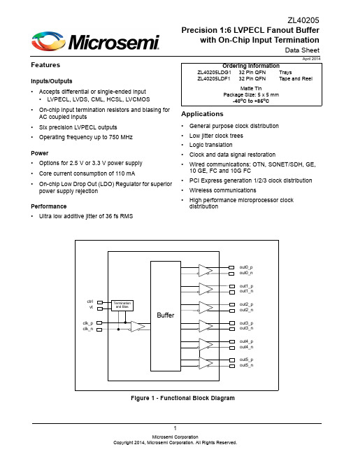
1FeaturesInputs/Outputs •Accepts differential or single-ended input •LVPECL, LVDS, CML, HCSL, LVCMOS •On-chip input termination resistors and biasing for AC coupled inputs•Six precision LVPECL outputs •Operating frequency up to 750 MHzPower •Options for 2.5 V or 3.3 V power supply •Core current consumption of 110 mA•On-chip Low Drop Out (LDO) Regulator for superior power supply rejectionPerformance •Ultra low additive jitter of 36 fs RMSApplications•General purpose clock distribution •Low jitter clock trees •Logic translation•Clock and data signal restoration•Wired communications: OTN, SONET/SDH, GE,10 GE, FC and 10G FC•PCI Express generation 1/2/3 clock distribution •Wireless communications•High performance microprocessor clock distributionApril 2014Figure 1 - Functional Block DiagramZL40205Precision 1:6 LVPECL Fanout Bufferwith On-Chip Input TerminationData SheetOrdering InformationZL40205LDG1 32 Pin QFN TraysZL40205LDF132 Pin QFNTape and ReelMatte TinPackage Size: 5 x 5 mm-40o C to +85o CTable of ContentsFeatures . . . . . . . . . . . . . . . . . . . . . . . . . . . . . . . . . . . . . . . . . . . . . . . . . . . . . . . . . . . . . . . . . . . . . . . . . . . . . . . . . 1 Inputs/Outputs . . . . . . . . . . . . . . . . . . . . . . . . . . . . . . . . . . . . . . . . . . . . . . . . . . . . . . . . . . . . . . . . . . . . . . . . .1 Power . . . . . . . . . . . . . . . . . . . . . . . . . . . . . . . . . . . . . . . . . . . . . . . . . . . . . . . . . . . . . . . . . . . . . . . . . . . . . . . .1 Performance . . . . . . . . . . . . . . . . . . . . . . . . . . . . . . . . . . . . . . . . . . . . . . . . . . . . . . . . . . . . . . . . . . . . . . . . . . .1 Applications . . . . . . . . . . . . . . . . . . . . . . . . . . . . . . . . . . . . . . . . . . . . . . . . . . . . . . . . . . . . . . . . . . . . . . . . . . . . . 1 Change Summary . . . . . . . . . . . . . . . . . . . . . . . . . . . . . . . . . . . . . . . . . . . . . . . . . . . . . . . . . . . . . . . . . . . . . . . . . 41.0 Package Description . . . . . . . . . . . . . . . . . . . . . . . . . . . . . . . . . . . . . . . . . . . . . . . . . . . . . . . . . . . . . . . . . . . .52.0 Pin Description. . . . . . . . . . . . . . . . . . . . . . . . . . . . . . . . . . . . . . . . . . . . . . . . . . . . . . . . . . . . . . . . . . . . . . . . .63.0 Functional Description . . . . . . . . . . . . . . . . . . . . . . . . . . . . . . . . . . . . . . . . . . . . . . . . . . . . . . . . . . . . . . . . . .73.1 Clock Inputs. . . . . . . . . . . . . . . . . . . . . . . . . . . . . . . . . . . . . . . . . . . . . . . . . . . . . . . . . . . . . . . . . . . . . . . . .73.2 Clock Outputs . . . . . . . . . . . . . . . . . . . . . . . . . . . . . . . . . . . . . . . . . . . . . . . . . . . . . . . . . . . . . . . . . . . . . .123.3 Device Additive Jitter. . . . . . . . . . . . . . . . . . . . . . . . . . . . . . . . . . . . . . . . . . . . . . . . . . . . . . . . . . . . . . . . .153.4 Power Supply . . . . . . . . . . . . . . . . . . . . . . . . . . . . . . . . . . . . . . . . . . . . . . . . . . . . . . . . . . . . . . . . . . . . . .163.4.1 Sensitivity to power supply noise. . . . . . . . . . . . . . . . . . . . . . . . . . . . . . . . . . . . . . . . . . . . . . . . . . .163.4.2 Power supply filtering. . . . . . . . . . . . . . . . . . . . . . . . . . . . . . . . . . . . . . . . . . . . . . . . . . . . . . . . . . . .163.4.3 PCB layout considerations. . . . . . . . . . . . . . . . . . . . . . . . . . . . . . . . . . . . . . . . . . . . . . . . . . . . . . . .164.0 AC and DC Electrical Characteristics . . . . . . . . . . . . . . . . . . . . . . . . . . . . . . . . . . . . . . . . . . . . . . . . . . . . .175.0 Performance Characterization . . . . . . . . . . . . . . . . . . . . . . . . . . . . . . . . . . . . . . . . . . . . . . . . . . . . . . . . . . .206.0 Typical Behavior . . . . . . . . . . . . . . . . . . . . . . . . . . . . . . . . . . . . . . . . . . . . . . . . . . . . . . . . . . . . . . . . . . . . . .217.0 Package Characteristics . . . . . . . . . . . . . . . . . . . . . . . . . . . . . . . . . . . . . . . . . . . . . . . . . . . . . . . . . . . . . . .238.0 Mechanical Drawing . . . . . . . . . . . . . . . . . . . . . . . . . . . . . . . . . . . . . . . . . . . . . . . . . . . . . . . . . . . . . . . . . . .24List of FiguresFigure 1 - Functional Block Diagram . . . . . . . . . . . . . . . . . . . . . . . . . . . . . . . . . . . . . . . . . . . . . . . . . . . . . . . . . . . . 1 Figure 2 - Pin Connections . . . . . . . . . . . . . . . . . . . . . . . . . . . . . . . . . . . . . . . . . . . . . . . . . . . . . . . . . . . . . . . . . . . 5 Figure 3 - Simplified Diagram of Input Stage. . . . . . . . . . . . . . . . . . . . . . . . . . . . . . . . . . . . . . . . . . . . . . . . . . . . . . 7 Figure 4 - Clock Input - LVPECL - DC Coupled. . . . . . . . . . . . . . . . . . . . . . . . . . . . . . . . . . . . . . . . . . . . . . . . . . . . 8 Figure 5 - Clock Input - LVPECL - AC Coupled. . . . . . . . . . . . . . . . . . . . . . . . . . . . . . . . . . . . . . . . . . . . . . . . . . . . 8 Figure 6 - Clock Input - LVDS - DC Coupled . . . . . . . . . . . . . . . . . . . . . . . . . . . . . . . . . . . . . . . . . . . . . . . . . . . . . . 9 Figure 7 - Clock Input - LVDS - AC Coupled . . . . . . . . . . . . . . . . . . . . . . . . . . . . . . . . . . . . . . . . . . . . . . . . . . . . . . 9 Figure 8 - Clock Input - CML- AC Coupled . . . . . . . . . . . . . . . . . . . . . . . . . . . . . . . . . . . . . . . . . . . . . . . . . . . . . . 10 Figure 9 - Clock Input - HCSL- AC Coupled . . . . . . . . . . . . . . . . . . . . . . . . . . . . . . . . . . . . . . . . . . . . . . . . . . . . . 10 Figure 10 - Clock Input - AC-coupled Single-Ended . . . . . . . . . . . . . . . . . . . . . . . . . . . . . . . . . . . . . . . . . . . . . . . 11 Figure 11 - Clock Input - DC-coupled 3.3V CMOS. . . . . . . . . . . . . . . . . . . . . . . . . . . . . . . . . . . . . . . . . . . . . . . . . 11 Figure 12 - Simplified Output Driver. . . . . . . . . . . . . . . . . . . . . . . . . . . . . . . . . . . . . . . . . . . . . . . . . . . . . . . . . . . . 12 Figure 13 - LVPECL Basic Output Termination . . . . . . . . . . . . . . . . . . . . . . . . . . . . . . . . . . . . . . . . . . . . . . . . . . . 12 Figure 14 - LVPECL Parallel Output Termination. . . . . . . . . . . . . . . . . . . . . . . . . . . . . . . . . . . . . . . . . . . . . . . . . . 13 Figure 15 - LVPECL Parallel Thevenin-Equivalent Output Termination. . . . . . . . . . . . . . . . . . . . . . . . . . . . . . . . . 13 Figure 16 - LVPECL AC Output Termination . . . . . . . . . . . . . . . . . . . . . . . . . . . . . . . . . . . . . . . . . . . . . . . . . . . . . 14 Figure 17 - LVPECL AC Output Termination for CML Inputs. . . . . . . . . . . . . . . . . . . . . . . . . . . . . . . . . . . . . . . . . 14 Figure 18 - Additive Jitter. . . . . . . . . . . . . . . . . . . . . . . . . . . . . . . . . . . . . . . . . . . . . . . . . . . . . . . . . . . . . . . . . . . . 15 Figure 19 - Decoupling Connections for Power Pins. . . . . . . . . . . . . . . . . . . . . . . . . . . . . . . . . . . . . . . . . . . . . . . 16 Figure 20 - Differential and Single-Ended Output Voltages Parameter Definitions . . . . . . . . . . . . . . . . . . . . . . . . 18 Figure 21 - Input To Output Timing . . . . . . . . . . . . . . . . . . . . . . . . . . . . . . . . . . . . . . . . . . . . . . . . . . . . . . . . . . . . 19Change SummaryPage Item Change1Applications Added PCI Express clock distribution.6Pin Description Added exposed pad to Pin Description.8Figure 4 and Figure 5Removed 22 ohm series resistors from Figure 4 and 5. These resistor are not required; however there is no impact to performance if the resistors are included.16Power supply filtering 18Figure 20Clarification of V ID and V OD .Below are the changes from the February 2013 issue to the April 2014 issue:Page Item Change8Figure 4Changed text to indicate the circuit is not recommended for VDD_driver=2.5V.Below are the changes from the November 2012 issue to the February 2013 issue:Corrected typo of 0.3 Ohm to 0.15 Ohm.1.0 Package DescriptionThe device is packaged in a 32 pin QFNFigure 2 - Pin Connections2.0 Pin DescriptionPin # Name Description3, 6clk_p, clk_n,Differential Input (Analog Input). Differential (or single ended) input signals.For all input configurations see “Clock Inputs” on page 728, 27, 26, 25, 24, 23, 18, 17, 16, 15, 14, 13out0_p, out0_nout1_p, out1_nout2_p, out2_nout3_p, out3_nout4_p, out4_nout5_p, out5_nDifferential Output (Analog Output). Differential outputs.9, 19,22, 32vdd Positive Supply Voltage. 2.5 V DC or 3.3 V DC nominal.1, 8vdd_core Positive Supply Voltage. 2.5 V DC or 3.3 V DC nominal.2, 7,20, 21gnd Ground. 0 V.4vt On-Chip Input Termination Node (Analog). Center tap between internal 50 Ohmtermination resistors.The use of this pin is detailed in section 3.1, “Clock Inputs“, for various input signal types.5ctrl Digital Control for On-Chip Input Termination (Input). Selects differential input mode;0: DC coupled LVPECL or LVDS modes1: AC coupled differential modesThis pin are internally pulled down to GND. The use of this pin is detailed in section 3.1,“Clock Inputs“, for various input signal types.10, 11,12, 29,30, 31NC No Connection. Leave unconnected.Exposed Pad Device GND.3.0 Functional DescriptionThe ZL40205 is an LVPECL clock fan out buffer with six output clock drivers capable of operating at frequencies up to 750MHz.The ZL40205 provides an internal input termination network for DC and AC coupled inputs; optional input biasing for AC coupled inputs is also provided. The ZL40205 can accept DC or AC coupled LVPECL and LVDS input signals, AC coupled CML or HCSL input signals, and single ended signals. A pin compatible device with external termination is also available.The ZL40205 is designed to fan out low-jitter reference clocks for wired or optical communications applications while adding minimal jitter to the clock signal. An internal linear power supply regulator and bulk capacitors minimize additive jitter due to power supply noise. The device operates from 2.5V+/-5% or 3.3V+/-5% supply. Its operation is guaranteed over the industrial temperature range -40°C to +85°C.The device block diagram is shown in Figure 1; its operation is described in the following sections.3.1 Clock InputsThe device has a differential input equipped with two on-chip 50 Ohm termination resistors arranged in series with a center tap. The input can accept many differential and single-ended signals with AC or DC coupling as appropriate. A control pin is available to enable internal biasing for AC coupled inputs. A block diagram of the input stage is in Figure 3.Receiverclk_n 50clk_pVt 50BiasctrlFigure 3 - Simplified Diagram of Input StageThis following figures give the components values and configuration for the various circuits compatible with the input stage and the use of the Vt and ctrl pins in each case.In the following diagrams where the ctrl pin is logically one and the Vt pin is not connected, the Vt pin can be instead connected to VDD with a capacitor. A capacitor can also help in Figure 4 between Vt and VDD. This capacitor will minimize the noise at the point between the two internal termination resistors and improve the overall performance of the device.Figure 4 - Clock Input - LVPECL - DC CoupledFigure 5 - Clock Input - LVPECL - AC CoupledFigure 6 - Clock Input - LVDS - DC CoupledFigure 7 - Clock Input - LVDS - AC CoupledFigure 8 - Clock Input - CML- AC CoupledFigure 9 - Clock Input - HCSL- AC CoupledFigure 10 - Clock Input - AC-coupled Single-EndedFigure 11 - Clock Input - DC-coupled 3.3V CMOS3.2 Clock OutputsLVPECL has a very low output impedance and a differential signal swing between 1V and 1.6 V. A simplified diagram for the output stage is shown in Figure 12.The LVPECL to LVDS output termination is not shown since there is a different device with the same inputs and LVDS outputs.out_pout_nFigure 12 - Simplified Output DriverThe methods to terminate the ZL40205 LVPECL drivers are shown in the following figures.Figure 15 - LVPECL Parallel Thevenin-Equivalent Output TerminationFigure 16 - LVPECL AC Output TerminationFigure 17 - LVPECL AC Output Termination for CML Inputs3.3 Device Additive JitterThe ZL40205 clock fanout buffer is not intended to filter clock jitter. The jitter performance of this type of device is characterized by its additive jitter. Additive jitter is the jitter the device would add to a hypothetical jitter-free clock as it passes through the device. The additive jitter of the ZL40205 is random and as such it is not correlated to the jitter of the input clock signal.The square of the resultant random RMS jitter at the output of the ZL40205 is equal to the sum of the squares of the various random RMS jitter sources including: input clock jitter; additive jitter of the buffer; and additive random jitter due to power supply noise. There may be additional deterministic jitter sources, but they are not shown in Figure 18.Figure 18 - Additive Jitter3.4 Power SupplyThis device operates employing either a 2.5V supply or 3.3V supply.3.4.1 Sensitivity to power supply noisePower supply noise from sources such as switching power supplies and high-power digital components such as FPGAs can induce additive jitter on clock buffer outputs. The ZL40205 is equipped with a low drop out (LDO) regulator and on-chip bulk capacitors to minimize additive jitter due to power supply noise. The on-chip regulation, recommended power supply filtering, and good PCB layout all work together to minimize the additive jitter from power supply noise.3.4.2 Power supply filteringJitter levels may increase when noise is present on the power pins. For optimal jitter performance, the device should be isolated from the power planes connected to its power supply pins as shown in Figure 19. •10 µF capacitors should be size 0603 or size 0805 X5R or X7R ceramic, 6.3 V minimum rating •0.1 µF capacitors should be size 0402 X5R ceramic, 6.3 V minimum rating •Capacitors should be placed next to the connected device power pins •A 0.15 Ohm resistor is recommended3.4.3 PCB layout considerationsThe power nets in Figure 19 can be implemented either as a plane island or routed power topology without changing the overall jitter performance of the device.ZL402051891922320.1 µF 0.1 µFvdd_core10 µF 0.1 µF0.15 Ωvdd0.1 µF 10 µFFigure 19 - Decoupling Connections for Power PinsAbsolute Maximum Ratings*Parameter Sym.Min.Max.Units 1Supply voltage V DD_R-0.5 4.6V 2Voltage on any digital pin V PIN-0.5VDD V 4LVPECL output current I out30mA 5Soldering temperature T260 °C 6Storage temperature T ST-55125 °C 7Junction temperature T j125 °C 8Voltage on input pin V input VDD V 9Input capacitance each pin C p500fF 4.0 AC and DC Electrical Characteristics* Exceeding these values may cause permanent damage. Functional operation under these conditions is not implied.* Voltages are with respect to ground (GND) unless otherwise statedRecommended Operating Conditions*Characteristics Sym.Min.Typ.Max.Units1Supply voltage 2.5 V mode V DD25 2.375 2.5 2.625V2Supply voltage 3.3 V mode V DD33 3.135 3.3 3.465V3Operating temperature T A-402585°C* Voltages are with respect to ground (GND) unless otherwise statedDC Electrical Characteristics - Current ConsumptionCharacteristics Sym.Min.Typ.Max.Units Notes 1Supply current LVPECL drivers -unloadedI dd_unload110mA Unloaded2Supply current LVPECL drivers - loaded (all outputs are active)I dd_load209mA Including powerto R L = 50DC Electrical Characteristics - Inputs and Outputs - for 3.3 V SupplyCharacteristics Sym.Min.Typ.Max.Units Notes1CMOS control logic high-level inputvoltageV CIH0.7*V DD V2CMOS control logic low-level inputvoltageV CIL0.3*V DD V3CMOS control logic Input leakagecurrentI IL1µA V I = V DD or 0 V4Differential input common modevoltageV CM 1.1 2.0V5Differential input voltage difference V ID0.251V6Differential input resistance V IR80100120ohm* This parameter was measured from 125 MHz to 750 MHz.* This parameter was measured from 125 MHz to 750 MHz.Figure 20 - Differential and Single-Ended Output Voltages Parameter Definitions7LVPECL output high voltage V OH V DD -1.40V 8LVPECL output low voltage V OL V DD - 1.62V 9LVPECL output differential voltage*V OD0.50.9VDC Electrical Characteristics - Inputs and Outputs - for 2.5 V SupplyCharacteristicsSym.Min.Typ.Max.Units Notes1Differential input common mode voltageV CM 1.1 1.6V 2Differential input voltage difference V ID 0.251V 3Differential input resistance V IR 80100120ohm 4LVPECL output high voltage V OH V DD -1.40V 5LVPECL output low voltage V OL V DD - 1.62V 6LVPECL output differential voltage*V OD0.40.9VDC Electrical Characteristics - Inputs and Outputs - for 3.3 V SupplyCharacteristicsSym.Min.Typ.Max.Units NotesAC Electrical Characteristics* - Inputs and Outputs (see Figure 21) - for 2.5/3.3 V supply.Characteristics Sym.Min.Typ.Max.Units Notes 1Maximum Operating Frequency1/t p750MHz2Input to output clock propagation delay t pd012ns3Output to output skew t out2out50100ps4Part to part output skew t part2part80300ps5Output clock Duty Cycle degradation t PWH/ t PWL-202Percent6LVPECL Output clock slew rate r SL0.75 1.2V/ns* Supply voltage and operating temperature are as per Recommended Operating ConditionsInputt Pt PWL t pdt PWHOutputFigure 21 - Input To Output TimingAdditive Jitter at 2.5 V*Output Frequency (MHz)Jitter MeasurementFilterTypical RMS (fs)Notes112512 kHz - 20 MHz 1392212.512 kHz - 20 MHz 1093311.0412 kHz - 20 MHz 85442512 kHz - 20 MHz 57550012 kHz - 20 MHz 506622.0812 kHz - 20 MHz 40775012 kHz - 20 MHz36Additive Jitter at 3.3 V*Output Frequency (MHz)Jitter MeasurementFilterTypical RMS (fs)Notes112512 kHz - 20 MHz 1152212.512 kHz - 20 MHz 853311.0412 kHz - 20 MHz 72442512 kHz - 20 MHz 55550012 kHz - 20 MHz 486622.0812 kHz - 20 MHz 41775012 kHz - 20 MHz395.0 Performance Characterization*The values in this table were taken with an approximate slew rate of 0.8 V/ns.*The values in this table were taken with an approximate slew rate of 0.8 V/ns.Additive Jitter from a Power Supply Tone*Carrier frequencyParameterTypicalUnitsNotes125MHz 25 mV at 100 kHz 115fs RMS 750MHz25 mV at 100 kHz59fs RMS* The values in this table are the additive periodic jitter caused by an interfering tone typically caused by a switching power supply. For this test, measurements were taken over the full temperature and voltage range for V DD = 2.5 V. The magnitude of the interfering tone is measured at the DUT.6.0 Typical BehaviorTypical Phase Noise at 622.08 MHzTypical Waveformat 155.52 MHzV OD versus FrequencyPropagation Delay versus TemperatureNote:This is for a single device. For more details see thePower Supply Tone Frequency (at 25 mV) versus PSRR at 125 MHz Power Supply Tone Frequency (at 25 mV) versus Additive Jitter at 125 MHzPower Supply Tone Magnitude (at 100 kHz) versus PSRR at 125 MHz Power Supply Tone Magnitude (at 100 kHz) versus Additive Jitter at 125 MHz7.0 Package CharacteristicsThermal DataParameter Symbol Test Condition Value UnitJunction to Ambient Thermal Resistance ΘJA Still Air1 m/s2 m/s 37.433.131.5o C/WJunction to Case Thermal Resistance ΘJC24.4o C/W Junction to Board Thermal Resistance ΘJB19.5o C/W Maximum Junction Temperature*T jmax125o C Maximum Ambient Temperature T A85o C© 2014 Microsemi Corporation. All rights reserved. Microsemi and the Microsemi logo are trademarks of Microsemi Corporation. All other trademarks and service marks are the property of their respective owners.Microsemi Corporation (NASDAQ: MSCC) offers a comprehensive portfolio of semiconductor and system solutions for communications, defense and security, aerospace and industrial markets. Products include high-performance and radiation-hardened analog mixed-signal integrated circuits, FPGAs, SoCs and ASICs; power management products; timing and synchronization devices and precise time solutions, setting the world’s standard for time; voice processing devices; RF solutions; discrete components; security technologies and scalable anti-tamper products; Power-over-Ethernet ICs and midspans; as well as custom design capabilities and services. Microsemi is headquartered in Aliso Viejo, Calif. and has approximately 3,400 employees globally. Learn more at .Microsemi Corporate Headquarters One One Enterprise, Aliso Viejo CA 92656 USA Within the USA: +1 (800) 713-4113Outside the USA: +1 (949) 380-6100Sales: +1 (949) 380-6136Fax: +1 (949) 215-4996E-mail: ***************************Information relating to products and services furnished herein by Microsemi Corporation or its subsidiaries (collectively “Microsemi”) is believed to be reliable. However, Microsemi assumes no liability for errors that may appear in this publication, or for liability otherwise arising from the application or use of any such information, product or service or for any infringement of patents or other intellectual property rights owned by third parties which may result from such application or use. Neither the supply of such information or purchase of product or service conveys any license, either express or implied, under patents or other intellectual property rights owned by Microsemi or licensed from third parties by Microsemi, whatsoever. Purchasers of products are also hereby notified that the use of product in certain ways or in combination with Microsemi, or non-Microsemi furnished goods or services may infringe patents or other intellectual property rights owned by Microsemi.This publication is issued to provide information only and (unless agreed by Microsemi in writing) may not be used, applied or reproduced for any purpose nor form part of any order or contract nor to be regarded as a representation relating to the products or services concerned. The products, their specifications, services and other information appearing in this publication are subject to change by Microsemi without notice. No warranty or guarantee express or implied is made regarding the capability, performance or suitability of any product or service. Information concerning possible methods of use is provided as a guide only and does not constitute any guarantee that such methods of use will be satisfactory in a specific piece of equipment. It is the user’s responsibility to fully determine the performance and suitability of any equipment using such information and to ensure that any publication or data used is up to date and has not been superseded. Manufacturing does not necessarily include testing of all functions or parameters. These products are not suitable for use in any medical and other products whose failure to perform may result in significant injury or death to the user. All products and materials are sold and services provided subject to Microsemi’s conditions of sale which are available on request.For more information about all Microsemi productsvisit our website at TECHNICAL DOCUMENTATION – NOT FOR RESALE。
华上芯片介绍
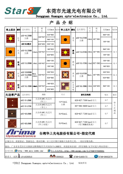
Dongguan Guangsu opto-electronics Co., Ltd.
产 品 介 绍
华上芯片 颜色 芯片型号:
尺 寸 波 长 亮度mcd 电压v
华上芯片 颜色 芯片型号:
尺 寸
波 长
亮度mcd 360-400
电压v
320-360 AOC-612RMM 620-627 红 主推 12miL 360-400 <2.4 光
<2.4
大功率产品
芯片型号:
规格
波长及亮度
电压
<2.7
备注
AOC-541RMM AOC-541YSM
大功率1W红光芯片 (华上) 大功率1W黄光芯片 (华上) 大功率1W红光芯片 (华上) 大功率1W红光芯片 (华上双线)
41*41miL 主推
620-627/7800(mcd)以上 587-592/6600(mcd)以上
公司主页: / 华上光电网址:/电话+886-3-3803801
联系人 :赵凯
13410238513
3500023
0769-81603478 版权所有
0769-89032879
©2012 Dongguan Guangsu.opto-electronics Co., Ltd.
AOC-S09RMM 主推
<2.4
320-360 460-520 <2.4 520-600
黄 光
AOC-S10YSM 9miL 587-592 主推
<2.4
320-360
红 AOC-614RMM 14miL 620-627 光
红 光 双 线 尺寸
AOC-H14RMM 14miL 620-630
850nm VCSEL—TOSA及其在高速通信中的应用

关键词 : 大数 据 ; 8 5 0 n m 垂 直腔 面发 射 激 光 器 一 传 输 光 组 件 ; 实 用化 ; 可靠性 ; 高 温 加速 寿命 试 验 中 图分 类 号 : T N2 5 3 文献标志码 : A 文章 编 号 : 1 0 0 5 - 8 7 8 8 ( 2 0 1 3 ) 0 4 - 0 0 4 9 - 0 4
r a t e s h o r t — wa v e l e n g t h s u b a s s e mb l y u s e d i n Et h e r n e t a n d l a r g e d a t a p r o c e s s i n g c e n t e r s . Th i s p a p e r i n t r o d u c e s t h e s t r u c t u r e , c h i p c h a r a c t e r i s t i c s ,t e c h n i c a l i n d e x e s a n d r e l e v a n t s t a n d a r d s f o r t h e p r a c t i c a l s u b a s s e mb l y,r e p o r t s t h e h i g h t e mp e r a t u r e a c c e l — e r a t e d l i f e t e s t c o n d i t i o n s f o r a n d r e s u l t s o f i t s c h i p s ,d i s c u s s e s t h e e f f e c t s o f v a r i a t i o n s i n s t r u c t u r e 。t e c h n o l o g y a n d e n v i r o n — me n t a l t e mp e r a t u r e o n i t s p e r f o r ma n c e s a n d p o i n t s o u t i t s a p p l i c a t i o n s i n t h e s h o r t - r a n g e E t h e r n e t a n d l a r g e d a t a p r o c e s s i n g
VIS Infinera 12x1 4x1 VCSEL芯片数据表说明书

No. 120314-Rev 1.0March 2012Product CParameter Typical NotesEmission Wavelength 850 nmavailable from 835 – 860 nm Data RateUp 28 Gbit/s per channel Rise time (20% to 80%) < 15 ps Threshold Current 1.0 mA Peak Output Power7 mWProduct Description Product DescriptionThese compact and very high modulation rate top-emitting GaAs-based vertical cavity surface emitting laser (VCSEL) chips and 1xN (N=1, 2, 4, 12, etc.) arrays are available as engineering samples for use in the development and evaluation of opticalinterconnections, optical backplanes and integrated waveguides, and next-generation optical data communications systems. The VCSELs are contacted on the top-surface individually using ground-source (GS) microprobes, wire bonds, or flip-chip bonds.DatasheetFeatures· available in 4x1 and 12x1configuration · up to 28 Gbit/s per channel · high temperature stability · standard pitch size 250 µm · high device-to-device uniformity Applications· 40/100 Gbit/s Ethernet · Infiniband FDR · OTU4 100 Gbit/s· Proprietary optical interconnects · Active Optical Cables (AOC)VI Systems GmbH Hardenbergstrasse 7 D-10623 Berlin28 Gbit/s VCSELs and VCSEL Arrays (850 nm)Product Code:V25B-850C 1x1 V25B -850C4 4x1 arrayV25B -850C12 12x1 arrayPreliminarySample image only. Actual product may vary.DatasheetV25B-850CPreliminary Electro Optical SpecificationsAbsolute Maximum RatingsAll product specifications and descriptions are subject to change without notice. VI Systems GmbH Hardenbergstrasse 7 D-10623 Berlin No. 120314-Rev 1.0 March 2012No. 120314-Rev 1.0March 2012DatasheetV15-850CPreliminaryVI Systems GmbH Hardenbergstrasse 7 D-10623 BerlinNo. 120314-Rev 1.0March 2012All product specifications and descriptions are subject to change without notice.Pleasecontactoursalesdepartmentforadditionalinformationandtoreceiveaquotation:*********************VI Systems GmbH Hardenbergstrasse 7 D-10623 BerlinThe V25B-850C has been tested to meet specifications outlined in this data sheet at room temperature. However, it has not undergone full qualification testing or characterization and therefore may not meet the performance specifications over all extremes.Limited Qualification NotificationVI Systems GmbH Hardenbergstrasse 7 10623 BerlinTel.: +49 30 3083143 30 Fax: +49 30 3083143 59 *********************DatasheetV25B-850C。
850nm VCSEL-TOSA及其在高速通信中的应用

850nm VCSEL-TOSA及其在高速通信中的应用丁国庆;孟海杰;胡长飞【摘要】高速、大数据容量传输和处理是光通信中的热点.10 Gbit/s 850 nm VCSEL-TOSA(垂直腔面发射激光器—传输光组件)是以太网和大数据处理中心所用的高速、短波长关键组件.文章介绍了实用化组件结构、芯片特点、技术指标及相关标准;报道了10 Gbit/s 850 nm VCSEL管芯高温加速寿命试验条件和结果;讨论了组件结构、工艺和环境温度变化对其性能的影响,指出了10 Gbit/s 850 nm VCSEL-TOSA在短途以太网和大数据收发、处理中心中的应用.【期刊名称】《光通信研究》【年(卷),期】2013(000)004【总页数】4页(P49-52)【关键词】大数据;850 nm垂直腔面发射激光器—传输光组件;实用化;可靠性;高温加速寿命试验【作者】丁国庆;孟海杰;胡长飞【作者单位】武汉华工正源光子技术有限公司,湖北武汉430223;武汉华工正源光子技术有限公司,湖北武汉430223;武汉华工正源光子技术有限公司,湖北武汉430223【正文语种】中文【中图分类】TN2530 引言随着视频和高速数据业务的不断发展,大数据容量传输、存储和处理的时代即将到来。
所谓大数据,是指无法在容许的时间内用常规软件工具对其内容进行抓取、管理和处理的数据集合,且大数据规模是不断变化的。
当前这种单一数据集的大小在几十TB和数PB之间。
现在有越来越多的网络终端,其收发数据的存储与管理不在终端完成,而是转移到数据中心去完成。
以云计算为标志的数据中心将是今后发展的重点之一。
对于短途、高速光网络(又称高速光以太网),国际上2010年6月正式发布了40 G/100 G以太网标准——IEEE 802.3ba[1],这里说的40 G/100 G, 不是单信道40 Gbit/s或100 Gbit/s,而是4个并行的10 Gbit/s 或10个并行的10 Gbit/s (或4个25 Gbit/s)。
微芯片技术(Microchip Technology) VSC8504-01数据手册说明书

VSC8504-01 Datasheet Quad-Port 10/100/1000BASE-T PHY with SynchronousEthernet and QSGMII/SGMII MACMicrosemi HeadquartersOne Enterprise, Aliso Viejo,CA 92656 USAWithin the USA: +1 (800) 713-4113 Outside the USA: +1 (949) 380-6100 Sales: +1 (949) 380-6136Fax: +1 (949) 215-4996Email: *************************** ©2018 Microsemi, a wholly owned subsidiary of Microchip Technology Inc. All rights reserved. Microsemi and the Microsemi logo are registered trademarks of Microsemi Corporation. All other trademarks and service marks are the property of their respective owners. Microsemi makes no warranty, representation, or guarantee regarding the information contained herein or the suitability of its products and services for any particular purpose, nor does Microsemi assume any liability whatsoever arising out of the application or use of any product or circuit. The products sold hereunder and any other products sold by Microsemi have been subject to limited testing and should not be used in conjunction with mission-critical equipment or applications. Any performance specifications are believed to be reliable but are not verified, and Buyer must conduct and complete all performance and other testing of the products, alone and together with, or installed in, any end-products. Buyer shall not rely on any data and performance specifications or parameters provided by Microsemi. It is the Buyer’s responsibility to independently determine suitability of any products and to test and verify the same. The information provided by Microsemi hereunder is provided “as is, where is” and with all faults, and the entire risk associated with such information is entirely with the Buyer. Microsemi does not grant, explicitly or implicitly, to any party any patent rights, licenses, or any other IP rights, whether with regard to such information itself or anything described by such information. Information provided in this document is proprietary to Microsemi, and Microsemi reserves the right to make any changes to the information in this document or to any products and services at any time without notice.About MicrosemiMicrosemi, a wholly owned subsidiary of Microchip Technology Inc. (Nasdaq: MCHP), offers a comprehensive portfolio of semiconductor and system solutions for aerospace & defense, communications, data center and industrial markets. Products include high-performance and radiation-hardened analog mixed-signal integrated circuits, FPGAs, SoCs and ASICs; power management products; timing and synchronization devices and precise time solutions, setting the world's standard for time; voice processing devices; RF solutions; discrete components; enterprise storage and communication solutions, security technologies and scalable anti-tamper products; Ethernet solutions; Power-over-Ethernet ICs andmidspans; as well as custom design capabilities and services. Learn more at .Contents1Revision History . . . . . . . . . . . . . . . . . . . . . . . . . . . . . . . . . . . . . . . . . . . . . . . . . . . . .11.1Revision4.3 . . . . . . . . . . . . . . . . . . . . . . . . . . . . . . . . . . . . . . . . . . . . . . . . . . . . . . . . . . . . . . . . . . . . . . . 11.2Revision4.2 . . . . . . . . . . . . . . . . . . . . . . . . . . . . . . . . . . . . . . . . . . . . . . . . . . . . . . . . . . . . . . . . . . . . . . . 11.3Revision 4.1 . . . . . . . . . . . . . . . . . . . . . . . . . . . . . . . . . . . . . . . . . . . . . . . . . . . . . . . . . . . . . . . . . . . . . . . 11.4Revision 4.0 . . . . . . . . . . . . . . . . . . . . . . . . . . . . . . . . . . . . . . . . . . . . . . . . . . . . . . . . . . . . . . . . . . . . . . . 11.5Revision2.0 . . . . . . . . . . . . . . . . . . . . . . . . . . . . . . . . . . . . . . . . . . . . . . . . . . . . . . . . . . . . . . . . . . . . . . . 12Product Overview . . . . . . . . . . . . . . . . . . . . . . . . . . . . . . . . . . . . . . . . . . . . . . . . . . .22.1Key Features . . . . . . . . . . . . . . . . . . . . . . . . . . . . . . . . . . . . . . . . . . . . . . . . . . . . . . . . . . . . . . . . . . . . . . 32.1.1Low Power . . . . . . . . . . . . . . . . . . . . . . . . . . . . . . . . . . . . . . . . . . . . . . . . . . . . . . . . . . . . . . . . . 32.1.2Advanced Carrier Ethernet Support . . . . . . . . . . . . . . . . . . . . . . . . . . . . . . . . . . . . . . . . . . . . . 32.1.3Wide Range of Support . . . . . . . . . . . . . . . . . . . . . . . . . . . . . . . . . . . . . . . . . . . . . . . . . . . . . . . 32.1.4Flexibility . . . . . . . . . . . . . . . . . . . . . . . . . . . . . . . . . . . . . . . . . . . . . . . . . . . . . . . . . . . . . . . . . . 32.2Block Diagram . . . . . . . . . . . . . . . . . . . . . . . . . . . . . . . . . . . . . . . . . . . . . . . . . . . . . . . . . . . . . . . . . . . . . 43Functional Descriptions . . . . . . . . . . . . . . . . . . . . . . . . . . . . . . . . . . . . . . . . . . . . . . .53.1Operating Modes . . . . . . . . . . . . . . . . . . . . . . . . . . . . . . . . . . . . . . . . . . . . . . . . . . . . . . . . . . . . . . . . . . . 53.1.1QSGMII/SGMII MAC-to-1000BASE-X Link Partner . . . . . . . . . . . . . . . . . . . . . . . . . . . . . . . . . 53.1.2QSGMII/SGMII MAC-to-100BASE-FX Link Partner . . . . . . . . . . . . . . . . . . . . . . . . . . . . . . . . . 73.1.3QSGMII/SGMII MAC-to-AMS and 1000BASE-X Media SerDes . . . . . . . . . . . . . . . . . . . . . . . . 73.1.4QSGMII/SGMII MAC-to-AMS and 100BASE-FX Media SerDes . . . . . . . . . . . . . . . . . . . . . . . . 83.1.5QSGMII/SGMII MAC-to-AMS and Protocol Transfer Mode . . . . . . . . . . . . . . . . . . . . . . . . . . . . 93.1.6QSGMII/SGMII MAC-to-Cat5 Link Partner . . . . . . . . . . . . . . . . . . . . . . . . . . . . . . . . . . . . . . . 103.1.7QSGMII/SGMII MAC-to-Protocol Transfer Mode . . . . . . . . . . . . . . . . . . . . . . . . . . . . . . . . . . . 103.1.81000BASE-X MAC-to-Cat5 Link Partner . . . . . . . . . . . . . . . . . . . . . . . . . . . . . . . . . . . . . . . . . 113.2SerDes MAC Interface . . . . . . . . . . . . . . . . . . . . . . . . . . . . . . . . . . . . . . . . . . . . . . . . . . . . . . . . . . . . . . 113.2.1SerDes MAC . . . . . . . . . . . . . . . . . . . . . . . . . . . . . . . . . . . . . . . . . . . . . . . . . . . . . . . . . . . . . . 123.2.2SGMII MAC . . . . . . . . . . . . . . . . . . . . . . . . . . . . . . . . . . . . . . . . . . . . . . . . . . . . . . . . . . . . . . . 123.2.3QSGMII MAC . . . . . . . . . . . . . . . . . . . . . . . . . . . . . . . . . . . . . . . . . . . . . . . . . . . . . . . . . . . . . . 123.3SerDes Media Interface . . . . . . . . . . . . . . . . . . . . . . . . . . . . . . . . . . . . . . . . . . . . . . . . . . . . . . . . . . . . . 133.3.1QSGMII/SGMII to 1000BASE-X . . . . . . . . . . . . . . . . . . . . . . . . . . . . . . . . . . . . . . . . . . . . . . . 133.3.2QSGMII/SGMII to 100BASE-FX . . . . . . . . . . . . . . . . . . . . . . . . . . . . . . . . . . . . . . . . . . . . . . . 133.3.3QSGMII to SGMII Protocol Conversion . . . . . . . . . . . . . . . . . . . . . . . . . . . . . . . . . . . . . . . . . . 143.3.4Unidirectional Transport for Fiber Media . . . . . . . . . . . . . . . . . . . . . . . . . . . . . . . . . . . . . . . . . 143.4PHY Addressing and Port Mapping . . . . . . . . . . . . . . . . . . . . . . . . . . . . . . . . . . . . . . . . . . . . . . . . . . . . 143.4.1PHY Addressing . . . . . . . . . . . . . . . . . . . . . . . . . . . . . . . . . . . . . . . . . . . . . . . . . . . . . . . . . . . 143.4.2SerDes Port Mapping . . . . . . . . . . . . . . . . . . . . . . . . . . . . . . . . . . . . . . . . . . . . . . . . . . . . . . . 143.5Cat5 Twisted Pair Media Interface . . . . . . . . . . . . . . . . . . . . . . . . . . . . . . . . . . . . . . . . . . . . . . . . . . . . . 143.5.1Voltage Mode Line Driver . . . . . . . . . . . . . . . . . . . . . . . . . . . . . . . . . . . . . . . . . . . . . . . . . . . . 153.5.2Cat5 Autonegotiation and Parallel Detection . . . . . . . . . . . . . . . . . . . . . . . . . . . . . . . . . . . . . . 153.5.3Automatic Crossover and Polarity Detection . . . . . . . . . . . . . . . . . . . . . . . . . . . . . . . . . . . . . . 153.5.4Manual HP Auto-MDIX Setting . . . . . . . . . . . . . . . . . . . . . . . . . . . . . . . . . . . . . . . . . . . . . . . . 163.5.5Link Speed Downshift . . . . . . . . . . . . . . . . . . . . . . . . . . . . . . . . . . . . . . . . . . . . . . . . . . . . . . . 163.5.6Energy Efficient Ethernet . . . . . . . . . . . . . . . . . . . . . . . . . . . . . . . . . . . . . . . . . . . . . . . . . . . . . 163.5.7Ring Resiliency . . . . . . . . . . . . . . . . . . . . . . . . . . . . . . . . . . . . . . . . . . . . . . . . . . . . . . . . . . . . 173.6Automatic Media Sense Interface Mode . . . . . . . . . . . . . . . . . . . . . . . . . . . . . . . . . . . . . . . . . . . . . . . . 173.7Reference Clock . . . . . . . . . . . . . . . . . . . . . . . . . . . . . . . . . . . . . . . . . . . . . . . . . . . . . . . . . . . . . . . . . . 183.7.1Configuring the Reference Clock . . . . . . . . . . . . . . . . . . . . . . . . . . . . . . . . . . . . . . . . . . . . . . . 183.7.2Single-Ended REFCLK Input . . . . . . . . . . . . . . . . . . . . . . . . . . . . . . . . . . . . . . . . . . . . . . . . . . 183.7.3Differential REFCLK Input . . . . . . . . . . . . . . . . . . . . . . . . . . . . . . . . . . . . . . . . . . . . . . . . . . . . 193.8Ethernet Inline Powered Devices . . . . . . . . . . . . . . . . . . . . . . . . . . . . . . . . . . . . . . . . . . . . . . . . . . . . . . 193.9IEEE 802.3af PoE Support . . . . . . . . . . . . . . . . . . . . . . . . . . . . . . . . . . . . . . . . . . . . . . . . . . . . . . . . . . 213.10ActiPHY Power Management . . . . . . . . . . . . . . . . . . . . . . . . . . . . . . . . . . . . . . . . . . . . . . . . . . . . . . . . 213.10.1Low Power State . . . . . . . . . . . . . . . . . . . . . . . . . . . . . . . . . . . . . . . . . . . . . . . . . . . . . . . . . . . 223.10.2Link Partner Wake-Up State . . . . . . . . . . . . . . . . . . . . . . . . . . . . . . . . . . . . . . . . . . . . . . . . . . 223.10.3Normal Operating State . . . . . . . . . . . . . . . . . . . . . . . . . . . . . . . . . . . . . . . . . . . . . . . . . . . . . . 223.11Media Recovered Clock Outputs . . . . . . . . . . . . . . . . . . . . . . . . . . . . . . . . . . . . . . . . . . . . . . . . . . . . . . 223.11.1Clock Selection Settings . . . . . . . . . . . . . . . . . . . . . . . . . . . . . . . . . . . . . . . . . . . . . . . . . . . . . 223.11.2Clock Output Squelch . . . . . . . . . . . . . . . . . . . . . . . . . . . . . . . . . . . . . . . . . . . . . . . . . . . . . . . 233.12Serial Management Interface . . . . . . . . . . . . . . . . . . . . . . . . . . . . . . . . . . . . . . . . . . . . . . . . . . . . . . . . . 233.12.1SMI Frames . . . . . . . . . . . . . . . . . . . . . . . . . . . . . . . . . . . . . . . . . . . . . . . . . . . . . . . . . . . . . . . 233.12.2SMI Interrupt . . . . . . . . . . . . . . . . . . . . . . . . . . . . . . . . . . . . . . . . . . . . . . . . . . . . . . . . . . . . . . 243.13LED Interface . . . . . . . . . . . . . . . . . . . . . . . . . . . . . . . . . . . . . . . . . . . . . . . . . . . . . . . . . . . . . . . . . . . . . 253.13.1LED Modes . . . . . . . . . . . . . . . . . . . . . . . . . . . . . . . . . . . . . . . . . . . . . . . . . . . . . . . . . . . . . . . 253.13.2Extended LED Modes . . . . . . . . . . . . . . . . . . . . . . . . . . . . . . . . . . . . . . . . . . . . . . . . . . . . . . . 273.13.3LED Behavior . . . . . . . . . . . . . . . . . . . . . . . . . . . . . . . . . . . . . . . . . . . . . . . . . . . . . . . . . . . . . 273.13.4Basic Serial LED Mode . . . . . . . . . . . . . . . . . . . . . . . . . . . . . . . . . . . . . . . . . . . . . . . . . . . . . . 283.13.5Enhanced Serial LED Mode . . . . . . . . . . . . . . . . . . . . . . . . . . . . . . . . . . . . . . . . . . . . . . . . . . 283.13.6LED Port Swapping . . . . . . . . . . . . . . . . . . . . . . . . . . . . . . . . . . . . . . . . . . . . . . . . . . . . . . . . . 293.14Fast Link Failure Indication . . . . . . . . . . . . . . . . . . . . . . . . . . . . . . . . . . . . . . . . . . . . . . . . . . . . . . . . . . 293.15Integrated Two-Wire Serial Multiplexer . . . . . . . . . . . . . . . . . . . . . . . . . . . . . . . . . . . . . . . . . . . . . . . . . 293.15.1Read/Write Access Using the Two-Wire Serial MUX . . . . . . . . . . . . . . . . . . . . . . . . . . . . . . . 303.16GPIO Pins . . . . . . . . . . . . . . . . . . . . . . . . . . . . . . . . . . . . . . . . . . . . . . . . . . . . . . . . . . . . . . . . . . . . . . . 313.17Testing Features . . . . . . . . . . . . . . . . . . . . . . . . . . . . . . . . . . . . . . . . . . . . . . . . . . . . . . . . . . . . . . . . . . 313.17.1Ethernet Packet Generator . . . . . . . . . . . . . . . . . . . . . . . . . . . . . . . . . . . . . . . . . . . . . . . . . . . 313.17.2CRC Counters . . . . . . . . . . . . . . . . . . . . . . . . . . . . . . . . . . . . . . . . . . . . . . . . . . . . . . . . . . . . . 323.17.3Far-End Loopback . . . . . . . . . . . . . . . . . . . . . . . . . . . . . . . . . . . . . . . . . . . . . . . . . . . . . . . . . . 323.17.4Near-End Loopback . . . . . . . . . . . . . . . . . . . . . . . . . . . . . . . . . . . . . . . . . . . . . . . . . . . . . . . . . 323.17.5Connector Loopback . . . . . . . . . . . . . . . . . . . . . . . . . . . . . . . . . . . . . . . . . . . . . . . . . . . . . . . . 333.17.6SerDes Loopbacks . . . . . . . . . . . . . . . . . . . . . . . . . . . . . . . . . . . . . . . . . . . . . . . . . . . . . . . . . 333.17.7VeriPHY Cable Diagnostics . . . . . . . . . . . . . . . . . . . . . . . . . . . . . . . . . . . . . . . . . . . . . . . . . . . 373.17.8JTAG Boundary Scan . . . . . . . . . . . . . . . . . . . . . . . . . . . . . . . . . . . . . . . . . . . . . . . . . . . . . . . 373.17.9JTAG Instruction Codes . . . . . . . . . . . . . . . . . . . . . . . . . . . . . . . . . . . . . . . . . . . . . . . . . . . . . 383.17.10Boundary Scan Register Cell Order . . . . . . . . . . . . . . . . . . . . . . . . . . . . . . . . . . . . . . . . . . . . 403.18100BASE-FX Halt Code Transmission and Reception . . . . . . . . . . . . . . . . . . . . . . . . . . . . . . . . . . . . . 403.19Configuration . . . . . . . . . . . . . . . . . . . . . . . . . . . . . . . . . . . . . . . . . . . . . . . . . . . . . . . . . . . . . . . . . . . . . 413.19.1Initialization . . . . . . . . . . . . . . . . . . . . . . . . . . . . . . . . . . . . . . . . . . . . . . . . . . . . . . . . . . . . . . . 424Registers . . . . . . . . . . . . . . . . . . . . . . . . . . . . . . . . . . . . . . . . . . . . . . . . . . . . . . . . .434.1Register and Bit Conventions . . . . . . . . . . . . . . . . . . . . . . . . . . . . . . . . . . . . . . . . . . . . . . . . . . . . . . . . 434.2IEEE802.3 and Main Registers . . . . . . . . . . . . . . . . . . . . . . . . . . . . . . . . . . . . . . . . . . . . . . . . . . . . . . . 444.2.1Mode Control . . . . . . . . . . . . . . . . . . . . . . . . . . . . . . . . . . . . . . . . . . . . . . . . . . . . . . . . . . . . . . 454.2.2Mode Status . . . . . . . . . . . . . . . . . . . . . . . . . . . . . . . . . . . . . . . . . . . . . . . . . . . . . . . . . . . . . . 464.2.3Device Identification . . . . . . . . . . . . . . . . . . . . . . . . . . . . . . . . . . . . . . . . . . . . . . . . . . . . . . . . 474.2.4Autonegotiation Advertisement . . . . . . . . . . . . . . . . . . . . . . . . . . . . . . . . . . . . . . . . . . . . . . . . 474.2.5Link Partner Autonegotiation Capability . . . . . . . . . . . . . . . . . . . . . . . . . . . . . . . . . . . . . . . . . 484.2.6Autonegotiation Expansion . . . . . . . . . . . . . . . . . . . . . . . . . . . . . . . . . . . . . . . . . . . . . . . . . . . 484.2.7Transmit Autonegotiation Next Page . . . . . . . . . . . . . . . . . . . . . . . . . . . . . . . . . . . . . . . . . . . . 494.2.8Autonegotiation Link Partner Next Page Receive . . . . . . . . . . . . . . . . . . . . . . . . . . . . . . . . . . 494.2.91000BASE-T Control . . . . . . . . . . . . . . . . . . . . . . . . . . . . . . . . . . . . . . . . . . . . . . . . . . . . . . . . 494.2.101000BASE-T Status . . . . . . . . . . . . . . . . . . . . . . . . . . . . . . . . . . . . . . . . . . . . . . . . . . . . . . . . 504.2.11MMD Access Control Register . . . . . . . . . . . . . . . . . . . . . . . . . . . . . . . . . . . . . . . . . . . . . . . . 514.2.12MMD Address or Data Register . . . . . . . . . . . . . . . . . . . . . . . . . . . . . . . . . . . . . . . . . . . . . . . . 514.2.131000BASE-T Status Extension 1 . . . . . . . . . . . . . . . . . . . . . . . . . . . . . . . . . . . . . . . . . . . . . . . 514.2.14100BASE-TX/FX Status Extension . . . . . . . . . . . . . . . . . . . . . . . . . . . . . . . . . . . . . . . . . . . . . 514.2.151000BASE-T Status Extension 2 . . . . . . . . . . . . . . . . . . . . . . . . . . . . . . . . . . . . . . . . . . . . . . . 524.2.16Bypass Control . . . . . . . . . . . . . . . . . . . . . . . . . . . . . . . . . . . . . . . . . . . . . . . . . . . . . . . . . . . . 534.2.18Error Counter 2 . . . . . . . . . . . . . . . . . . . . . . . . . . . . . . . . . . . . . . . . . . . . . . . . . . . . . . . . . . . . 544.2.19Error Counter 3 . . . . . . . . . . . . . . . . . . . . . . . . . . . . . . . . . . . . . . . . . . . . . . . . . . . . . . . . . . . . 544.2.20Extended Control and Status . . . . . . . . . . . . . . . . . . . . . . . . . . . . . . . . . . . . . . . . . . . . . . . . . . 544.2.21Extended PHY Control Set 1 . . . . . . . . . . . . . . . . . . . . . . . . . . . . . . . . . . . . . . . . . . . . . . . . . . 554.2.22Extended PHY Control Set 2 . . . . . . . . . . . . . . . . . . . . . . . . . . . . . . . . . . . . . . . . . . . . . . . . . . 564.2.23Interrupt Mask . . . . . . . . . . . . . . . . . . . . . . . . . . . . . . . . . . . . . . . . . . . . . . . . . . . . . . . . . . . . . 574.2.24Interrupt Status . . . . . . . . . . . . . . . . . . . . . . . . . . . . . . . . . . . . . . . . . . . . . . . . . . . . . . . . . . . . 584.2.25Device Auxiliary Control and Status . . . . . . . . . . . . . . . . . . . . . . . . . . . . . . . . . . . . . . . . . . . . 584.2.26LED Mode Select . . . . . . . . . . . . . . . . . . . . . . . . . . . . . . . . . . . . . . . . . . . . . . . . . . . . . . . . . . . 594.2.27LED Behavior . . . . . . . . . . . . . . . . . . . . . . . . . . . . . . . . . . . . . . . . . . . . . . . . . . . . . . . . . . . . . 604.2.28Extended Page Access . . . . . . . . . . . . . . . . . . . . . . . . . . . . . . . . . . . . . . . . . . . . . . . . . . . . . . 61 4.3Extended Page 1 Registers . . . . . . . . . . . . . . . . . . . . . . . . . . . . . . . . . . . . . . . . . . . . . . . . . . . . . . . . . . 614.3.1SerDes Media Control . . . . . . . . . . . . . . . . . . . . . . . . . . . . . . . . . . . . . . . . . . . . . . . . . . . . . . . 624.3.2Cu Media CRC Good Counter . . . . . . . . . . . . . . . . . . . . . . . . . . . . . . . . . . . . . . . . . . . . . . . . . 624.3.3Extended Mode Control . . . . . . . . . . . . . . . . . . . . . . . . . . . . . . . . . . . . . . . . . . . . . . . . . . . . . . 634.3.4ActiPHY Control . . . . . . . . . . . . . . . . . . . . . . . . . . . . . . . . . . . . . . . . . . . . . . . . . . . . . . . . . . . . 634.3.5PoE and Miscellaneous Functionality . . . . . . . . . . . . . . . . . . . . . . . . . . . . . . . . . . . . . . . . . . . 654.3.6Ethernet Packet Generator Control 1 . . . . . . . . . . . . . . . . . . . . . . . . . . . . . . . . . . . . . . . . . . . 654.3.7Ethernet Packet Generator Control 2 . . . . . . . . . . . . . . . . . . . . . . . . . . . . . . . . . . . . . . . . . . . 66 4.4Extended Page 2 Registers . . . . . . . . . . . . . . . . . . . . . . . . . . . . . . . . . . . . . . . . . . . . . . . . . . . . . . . . . . 664.4.1Cu PMD Transmit Control . . . . . . . . . . . . . . . . . . . . . . . . . . . . . . . . . . . . . . . . . . . . . . . . . . . . 664.4.2EEE Control . . . . . . . . . . . . . . . . . . . . . . . . . . . . . . . . . . . . . . . . . . . . . . . . . . . . . . . . . . . . . . . 684.4.3Ring Resiliency Control . . . . . . . . . . . . . . . . . . . . . . . . . . . . . . . . . . . . . . . . . . . . . . . . . . . . . . 69 4.5Extended Page 3 Registers . . . . . . . . . . . . . . . . . . . . . . . . . . . . . . . . . . . . . . . . . . . . . . . . . . . . . . . . . . 704.5.1MAC SerDes PCS Control . . . . . . . . . . . . . . . . . . . . . . . . . . . . . . . . . . . . . . . . . . . . . . . . . . . . 704.5.2MAC SerDes PCS Status . . . . . . . . . . . . . . . . . . . . . . . . . . . . . . . . . . . . . . . . . . . . . . . . . . . . 714.5.3MAC SerDes Clause 37 Advertised Ability . . . . . . . . . . . . . . . . . . . . . . . . . . . . . . . . . . . . . . . 724.5.4MAC SerDes Clause 37 Link Partner Ability . . . . . . . . . . . . . . . . . . . . . . . . . . . . . . . . . . . . . . 724.5.5MAC SerDes Status . . . . . . . . . . . . . . . . . . . . . . . . . . . . . . . . . . . . . . . . . . . . . . . . . . . . . . . . 724.5.6Media SerDes Transmit Good Packet Counter . . . . . . . . . . . . . . . . . . . . . . . . . . . . . . . . . . . . 734.5.7Media SerDes Transmit CRC Error Counter . . . . . . . . . . . . . . . . . . . . . . . . . . . . . . . . . . . . . . 734.5.8Media SerDes PCS Control . . . . . . . . . . . . . . . . . . . . . . . . . . . . . . . . . . . . . . . . . . . . . . . . . . . 734.5.9Media SerDes PCS Status . . . . . . . . . . . . . . . . . . . . . . . . . . . . . . . . . . . . . . . . . . . . . . . . . . . 744.5.10Media SerDes Clause 37 Advertised Ability . . . . . . . . . . . . . . . . . . . . . . . . . . . . . . . . . . . . . . 744.5.11Media SerDes Clause 37 Link Partner Ability . . . . . . . . . . . . . . . . . . . . . . . . . . . . . . . . . . . . . 744.5.12Media SerDes Status . . . . . . . . . . . . . . . . . . . . . . . . . . . . . . . . . . . . . . . . . . . . . . . . . . . . . . . . 754.5.13Fiber Media CRC Good Counter . . . . . . . . . . . . . . . . . . . . . . . . . . . . . . . . . . . . . . . . . . . . . . . 754.5.14Fiber Media CRC Error Counter . . . . . . . . . . . . . . . . . . . . . . . . . . . . . . . . . . . . . . . . . . . . . . . 75 4.6General Purpose Registers . . . . . . . . . . . . . . . . . . . . . . . . . . . . . . . . . . . . . . . . . . . . . . . . . . . . . . . . . . 754.6.1Reserved General Purpose Address Space . . . . . . . . . . . . . . . . . . . . . . . . . . . . . . . . . . . . . . 764.6.2SIGDET/GPIO Control . . . . . . . . . . . . . . . . . . . . . . . . . . . . . . . . . . . . . . . . . . . . . . . . . . . . . . . 764.6.3GPIO Control 2 . . . . . . . . . . . . . . . . . . . . . . . . . . . . . . . . . . . . . . . . . . . . . . . . . . . . . . . . . . . . 774.6.4GPIO Input . . . . . . . . . . . . . . . . . . . . . . . . . . . . . . . . . . . . . . . . . . . . . . . . . . . . . . . . . . . . . . . . 784.6.5GPIO Output . . . . . . . . . . . . . . . . . . . . . . . . . . . . . . . . . . . . . . . . . . . . . . . . . . . . . . . . . . . . . . 794.6.6GPIO Pin Configuration . . . . . . . . . . . . . . . . . . . . . . . . . . . . . . . . . . . . . . . . . . . . . . . . . . . . . . 794.6.7Microprocessor Command . . . . . . . . . . . . . . . . . . . . . . . . . . . . . . . . . . . . . . . . . . . . . . . . . . . 804.6.8MAC Configuration and Fast Link . . . . . . . . . . . . . . . . . . . . . . . . . . . . . . . . . . . . . . . . . . . . . . 804.6.9Two-Wire Serial MUX Control 1 . . . . . . . . . . . . . . . . . . . . . . . . . . . . . . . . . . . . . . . . . . . . . . . 814.6.10Two-Wire Serial MUX Control 2 . . . . . . . . . . . . . . . . . . . . . . . . . . . . . . . . . . . . . . . . . . . . . . . 814.6.11Two-Wire Serial MUX Data Read/Write . . . . . . . . . . . . . . . . . . . . . . . . . . . . . . . . . . . . . . . . . . 824.6.12Recovered Clock 1 Control . . . . . . . . . . . . . . . . . . . . . . . . . . . . . . . . . . . . . . . . . . . . . . . . . . . 824.6.13Recovered Clock 2 Control . . . . . . . . . . . . . . . . . . . . . . . . . . . . . . . . . . . . . . . . . . . . . . . . . . . 834.6.14Enhanced LED Control . . . . . . . . . . . . . . . . . . . . . . . . . . . . . . . . . . . . . . . . . . . . . . . . . . . . . . 844.6.15Global Interrupt Status . . . . . . . . . . . . . . . . . . . . . . . . . . . . . . . . . . . . . . . . . . . . . . . . . . . . . . . 85 4.7Clause 45 Registers to Support Energy Efficient Ethernet and 802.3bf . . . . . . . . . . . . . . . . . . . . . . . . 864.7.1PCS Status 1 . . . . . . . . . . . . . . . . . . . . . . . . . . . . . . . . . . . . . . . . . . . . . . . . . . . . . . . . . . . . . . 864.7.2EEE Capability . . . . . . . . . . . . . . . . . . . . . . . . . . . . . . . . . . . . . . . . . . . . . . . . . . . . . . . . . . . . . 874.7.4EEE Advertisement . . . . . . . . . . . . . . . . . . . . . . . . . . . . . . . . . . . . . . . . . . . . . . . . . . . . . . . . . 874.7.5EEE Link Partner Advertisement . . . . . . . . . . . . . . . . . . . . . . . . . . . . . . . . . . . . . . . . . . . . . . . 875Electrical Specifications . . . . . . . . . . . . . . . . . . . . . . . . . . . . . . . . . . . . . . . . . . . . . .895.1DC Characteristics . . . . . . . . . . . . . . . . . . . . . . . . . . . . . . . . . . . . . . . . . . . . . . . . . . . . . . . . . . . . . . . . . 895.1.1VDD25 . . . . . . . . . . . . . . . . . . . . . . . . . . . . . . . . . . . . . . . . . . . . . . . . . . . . . . . . . . . . . . . . . . . 895.1.2LED and GPIO . . . . . . . . . . . . . . . . . . . . . . . . . . . . . . . . . . . . . . . . . . . . . . . . . . . . . . . . . . . . . 895.1.3Internal Pull-Up or Pull-Down Resistors . . . . . . . . . . . . . . . . . . . . . . . . . . . . . . . . . . . . . . . . . 895.1.4Reference Clock . . . . . . . . . . . . . . . . . . . . . . . . . . . . . . . . . . . . . . . . . . . . . . . . . . . . . . . . . . . 905.1.5SerDes Interface (SGMII) . . . . . . . . . . . . . . . . . . . . . . . . . . . . . . . . . . . . . . . . . . . . . . . . . . . . 905.1.6Enhanced SerDes Interface (QSGMII) . . . . . . . . . . . . . . . . . . . . . . . . . . . . . . . . . . . . . . . . . . 925.1.7Current Consumption . . . . . . . . . . . . . . . . . . . . . . . . . . . . . . . . . . . . . . . . . . . . . . . . . . . . . . . 935.1.8Thermal Diode . . . . . . . . . . . . . . . . . . . . . . . . . . . . . . . . . . . . . . . . . . . . . . . . . . . . . . . . . . . . . 945.2AC Characteristics . . . . . . . . . . . . . . . . . . . . . . . . . . . . . . . . . . . . . . . . . . . . . . . . . . . . . . . . . . . . . . . . . 945.2.1Reference Clock . . . . . . . . . . . . . . . . . . . . . . . . . . . . . . . . . . . . . . . . . . . . . . . . . . . . . . . . . . . 945.2.2Recovered Clock . . . . . . . . . . . . . . . . . . . . . . . . . . . . . . . . . . . . . . . . . . . . . . . . . . . . . . . . . . . 955.2.3SerDes Outputs . . . . . . . . . . . . . . . . . . . . . . . . . . . . . . . . . . . . . . . . . . . . . . . . . . . . . . . . . . . . 965.2.4SerDes Driver Jitter . . . . . . . . . . . . . . . . . . . . . . . . . . . . . . . . . . . . . . . . . . . . . . . . . . . . . . . . . 975.2.5SerDes Inputs . . . . . . . . . . . . . . . . . . . . . . . . . . . . . . . . . . . . . . . . . . . . . . . . . . . . . . . . . . . . . 975.2.6SerDes Receiver Jitter Tolerance . . . . . . . . . . . . . . . . . . . . . . . . . . . . . . . . . . . . . . . . . . . . . . 975.2.7Enhanced SerDes Interface . . . . . . . . . . . . . . . . . . . . . . . . . . . . . . . . . . . . . . . . . . . . . . . . . . 975.2.8Basic Serial LEDs . . . . . . . . . . . . . . . . . . . . . . . . . . . . . . . . . . . . . . . . . . . . . . . . . . . . . . . . . 1005.2.9Enhanced Serial LEDs . . . . . . . . . . . . . . . . . . . . . . . . . . . . . . . . . . . . . . . . . . . . . . . . . . . . . 1005.2.10JTAG Interface . . . . . . . . . . . . . . . . . . . . . . . . . . . . . . . . . . . . . . . . . . . . . . . . . . . . . . . . . . . 1015.2.11Serial Management Interface . . . . . . . . . . . . . . . . . . . . . . . . . . . . . . . . . . . . . . . . . . . . . . . . 1025.2.12Reset Timing . . . . . . . . . . . . . . . . . . . . . . . . . . . . . . . . . . . . . . . . . . . . . . . . . . . . . . . . . . . . . 1035.3Operating Conditions . . . . . . . . . . . . . . . . . . . . . . . . . . . . . . . . . . . . . . . . . . . . . . . . . . . . . . . . . . . . . . 1045.4Stress Ratings . . . . . . . . . . . . . . . . . . . . . . . . . . . . . . . . . . . . . . . . . . . . . . . . . . . . . . . . . . . . . . . . . . . 1046Pin Descriptions . . . . . . . . . . . . . . . . . . . . . . . . . . . . . . . . . . . . . . . . . . . . . . . . . . .1056.1Pin Identifications . . . . . . . . . . . . . . . . . . . . . . . . . . . . . . . . . . . . . . . . . . . . . . . . . . . . . . . . . . . . . . . . . 1056.2Pin Diagram . . . . . . . . . . . . . . . . . . . . . . . . . . . . . . . . . . . . . . . . . . . . . . . . . . . . . . . . . . . . . . . . . . . . . 1056.3Pins by Function . . . . . . . . . . . . . . . . . . . . . . . . . . . . . . . . . . . . . . . . . . . . . . . . . . . . . . . . . . . . . . . . . 1076.3.1GPIO and SIGDET . . . . . . . . . . . . . . . . . . . . . . . . . . . . . . . . . . . . . . . . . . . . . . . . . . . . . . . . 1086.3.2JTAG . . . . . . . . . . . . . . . . . . . . . . . . . . . . . . . . . . . . . . . . . . . . . . . . . . . . . . . . . . . . . . . . . . . 1086.3.3Miscellaneous . . . . . . . . . . . . . . . . . . . . . . . . . . . . . . . . . . . . . . . . . . . . . . . . . . . . . . . . . . . . 1086.3.4Power Supply . . . . . . . . . . . . . . . . . . . . . . . . . . . . . . . . . . . . . . . . . . . . . . . . . . . . . . . . . . . . 1096.3.5SGMII/SerDes/QSGMII MAC Interface . . . . . . . . . . . . . . . . . . . . . . . . . . . . . . . . . . . . . . . . . 1106.3.6SerDes Media Interface . . . . . . . . . . . . . . . . . . . . . . . . . . . . . . . . . . . . . . . . . . . . . . . . . . . . . 1116.3.7Serial Management Interface . . . . . . . . . . . . . . . . . . . . . . . . . . . . . . . . . . . . . . . . . . . . . . . . 1116.3.8Twisted Pair Interface . . . . . . . . . . . . . . . . . . . . . . . . . . . . . . . . . . . . . . . . . . . . . . . . . . . . . . 1126.4Pins by Number . . . . . . . . . . . . . . . . . . . . . . . . . . . . . . . . . . . . . . . . . . . . . . . . . . . . . . . . . . . . . . . . . . 1136.5Pins by Name . . . . . . . . . . . . . . . . . . . . . . . . . . . . . . . . . . . . . . . . . . . . . . . . . . . . . . . . . . . . . . . . . . . . 1167Package Information . . . . . . . . . . . . . . . . . . . . . . . . . . . . . . . . . . . . . . . . . . . . . . .1197.1Package Drawing . . . . . . . . . . . . . . . . . . . . . . . . . . . . . . . . . . . . . . . . . . . . . . . . . . . . . . . . . . . . . . . . . 1197.2Thermal Specifications . . . . . . . . . . . . . . . . . . . . . . . . . . . . . . . . . . . . . . . . . . . . . . . . . . . . . . . . . . . . . 1207.3Moisture Sensitivity . . . . . . . . . . . . . . . . . . . . . . . . . . . . . . . . . . . . . . . . . . . . . . . . . . . . . . . . . . . . . . . 1218Design Considerations . . . . . . . . . . . . . . . . . . . . . . . . . . . . . . . . . . . . . . . . . . . . .1228.1AMS and 100BASE-FX . . . . . . . . . . . . . . . . . . . . . . . . . . . . . . . . . . . . . . . . . . . . . . . . . . . . . . . . . . . . 1228.210BASE-T signal amplitude . . . . . . . . . . . . . . . . . . . . . . . . . . . . . . . . . . . . . . . . . . . . . . . . . . . . . . . . . 1228.3SNR degradation and link drops . . . . . . . . . . . . . . . . . . . . . . . . . . . . . . . . . . . . . . . . . . . . . . . . . . . . . 1228.4Clause 45 register 3.22 . . . . . . . . . . . . . . . . . . . . . . . . . . . . . . . . . . . . . . . . . . . . . . . . . . . . . . . . . . . . 122。
OPV300 OPV310 OPV314系列850nm垂直光吸收激光器(VCSEL)产品说明书

Vertical Cavity Surface Emitting Laser OPV300, OPV310, OPV310Y, OPV314, OPV314YDescription:The OPV300 / OPV310 / OPV314 series are high performance 850nm Vertical Cavity Surface Emitting Laser (VCSEL). The OPV300 and OPV310 are designed to be utilized for sensing applications as well as air transmission of data. The OPV314 is designed for high speed communication links. The OPV310 / OPV314 combine all the performance advantages of a VCSEL with the addition of a power monitor diode for precise control of optical power. The OPV310 and OPV314 have a back monitor photodiode used for optical power management or optical reception for data communication applications.The OPV300 / OPV310 have a flat lens while the OPV314 has a microbead lens. Refer to mechanical drawings for details.The high performance 850nm VCSEL is designed for applications where low current is required with high on -axis optical power. These product ’s combine features including high speed, high output optical power and concentric beam making it an ideal transmitter for integration into all types of data communications equipment as well as for reflective and transmissive switches.Applications:• Fiber Channel • Gigabit Ethernet • ATM • VSR• Intra -System links• Optical backplane interconnects • Reflective sensing • Interruptive sensing•Long distance spot illuminationFeatures:• 850nm VCSEL Technology • Data rates up to 2.5 Gbps • High thermal stability• Low drive current / high output density • Narrow and concentric beam angle• Recommended for multimode fiber applications •Burned in for communication level reliabilityRoHSAdditional laser safety information can be found on the Optek website. See application bulletin #221.Classification is not marked on the device due to space limitations. See package outline for centerline of optical radiance. Operating devices beyond maximum rating may result in hazardous radiation exposure.OPV314YAbsolute Maximum Ratings (T A = 25° C unless otherwise noted)Electrical SpecificationsNotes:(1) Threshold Current is based on the two line intersection method specified in Telcordia GR -468-Core. Line 1 from 4 mA to 6 mA. Line 2 from 0 mA to 0.5 mA.(2) Series Resistance is the slope of the Voltage -Current line from 5 to 8 mA.(3) Slope efficiency is the slope of the best fit LI line from 5 mA to 8 mA using no larger than .25 mAtest interval points.(4) Using data points taken for slope efficiency above, delta L/delta I shall be calculated for eachadjacent pair of points.Additional laser safety information can be found on the Optek website. See application bulletin #221.Classification is not marked on the device due to space limitations. See package outline for centerline of optical radiance. Operating devices beyond maximum rating may result in hazardous radiation exposure.OPV314YElectrical SpecificationsElectrical Characteristics (T A = 25° C unless otherwise noted)(1)Threshold Current is based on the two line intersection method specified in Telcordia GR-468-Core. Line 1 from 4 mA to 6 mA. Line 2from 0 mA to 0.5 mA.(2)Series Resistance is the slope of the Voltage-Current line from 5 to 8 mA.(3)Slope efficiency, is the slope of the best fit LI line from 5 mA to 8 mA using no larger than .25 mA test interval points.(4)Using data points taken for slope efficiency above, delta L/delta I shall be calculated for each adjacent pair of points.(5)ESD Class 1OPV314YNormalized Output Power vs. Forward CurrentN o r m a l i z e d O u t p u t P o w e r (7m A , 25 °C )PerformanceForward Current (mA)OPV314Y1 2 3 VCSEL PDVCSEL PD1 2 VCSEL OPV300 & OPV310PerformanceOPV314Y1) Tolerances are ±0.005 unlessotherwise specified2) Dimensions in inches [mm]OPV3141 2 3 VCSEL PDVCSEL PD。
- 1、下载文档前请自行甄别文档内容的完整性,平台不提供额外的编辑、内容补充、找答案等附加服务。
- 2、"仅部分预览"的文档,不可在线预览部分如存在完整性等问题,可反馈申请退款(可完整预览的文档不适用该条件!)。
- 3、如文档侵犯您的权益,请联系客服反馈,我们会尽快为您处理(人工客服工作时间:9:00-18:30)。
1x1/4/12 chip
Vertical Cavity Surface-Emitting Laser Cathode on top side Unsealed 85% r.H./85° C certified 1x1, 1x4, 1x12 chips
ELECTRO-OPTICAL CHARACTERISTICS
VCSEL-ULM850-14-chips-v01
- 40 .. 125° C 0 .. 85° C 20 mW 12 mA 8V 6mW
NOTICE: Stresses greater than those listed under „Absolute Maximum Ratings“ may cause permanent damage to the device. These are stress ratings only and functional operation of the device at these or any other condition beyond those indicated for extended periods of time may effect device reliability. ATTENTION: Electrostatic Sensitive Devices Observe Precautions for Handling
Units: µm
VCSEL line arrays:
Description: Type: Wiring: Dimensions: Thickness: 1 x 12 VCSEL line array ULM850-14-TT-N0112U common cathodes 235 um x 2985 um 150 um 1 x 4 VCSEL line array ULM850-14-TT-N0104U common cathodes 235 um x 985 um 150 um
INVISIBLE LASER RADIATION AVOID BEAM EXPOSURE CLASS 3B LASER PRODUCT
Pre = 25° C unless otherwise stated. PARAMETER Emission wavelength Threshold current Threshold voltage Slope Efficiency Variation of ηs over temp. Laser forward current Differential series resistance 3dB modulation bandwidth Rise and fall time Relative intensity noise Wavelength tuning over current Wavelength tuning over temp. Thermal resistance Beam divergence Spectral bandwidth RThermal θ ∆λ 1 SYMBOL UNITS MIN λR Ith Uth ηs Iop RS_25 ν3dB t R /t F 20/80 RIN nm mA V W/A mA Ω GHz ps dB/Hz nm/mA nm/K K/mW ° nm 20 0.3 0.07 2.5 30 1/exp², Popt. = 1.5mW 0.65 Popt = 1.5 mW 3.0 1.4 0.4 -0.5 4.4 50 11 30 -128 Tchip = 0...85° C 6.0 Popt = 1.5 mW Popt = 1.5 mW Popt = 1.5 mW Popt = 1.5 mW 840 TYP MAX TEST CONDITIONS 850 0.6 1.8 860 Popt = 1.5 mW
Single VCSEL chip:
Description: Type: Mounting: Dimensions: Thickness: VCSEL chip, single channel ULM850-14-TT-N0101U anode and cathode wire bonding on front side 235 um x 235 um 150 um
∆ηs / ηs / ∆ T %/° C
ABSOLUTE MAXIMUM RATINGS
Storage temperature Operating temperature Electrical power dissipation Continous forward current Reverse voltage Optical output power