NRLM103M80V22X45F中文资料
LM103中文资料

Original Creation Date: 12/02/96Last Update Date: 12/20/96Last Major Revision Date: 12/02/96MNLM103-3.0-H REV 0A0MILITARY DATA SHEETREFERENCE DIODEGeneral DescriptionThe LM103 is a two-terminal monolithic reference diode electrically equivalent to a breakdown diode. The device makes use of the reverse punch-through of double-diffused transistors, combined with active circuitry, to produce a breakdown characteristic which is ten times sharper than single-junction zener diodes at low voltages. Breakdown voltages from 3.0V to 3.9V are available; and, although the design is optimized foroperation between 100uA and 1mA, it is completely specified from 10uA to 10mA. Noteworthy features of the device are:- Exceptionally sharp breakdown- Low dynamic impedance from 10uA to 10mA- Planar, passivated junctions for stable operation - Low capacitanceThe LM103, is useful in a wide range of circuit applications from level shifting to simple voltage regulation. It can also be employed with operational amplifiers in producingbreakpoints to generate nonlinear transfer functions. Finally, its unique characteristics recommend it as a reference element in low voltage power supplies with input voltages down to 4V.NS Part NumbersLM103H-3.0-SMD*LM103H-3.0/883Industry Part NumberLM103Prime DieLM103Controlling Document7702806XA*ProcessingMIL-STD-883, Method 5004Quality Conformance InspectionMIL-STD-883, Method 5005Subgrp Description Temp ( C)o 1Static tests at +252Static tests at +1253Static tests at -554Dynamic tests at +255Dynamic tests at +1256Dynamic tests at -557Functional tests at +258A Functional tests at +1258B Functional tests at -559Switching tests at +2510Switching tests at +12511Switching tests at-55MILITARY DATA SHEET MNLM103-3.0-H REV 0A0(Absolute Maximum Ratings)(Note 1)Power Dissipation(Note 2)250mWReverse Current20mAForward Current100mAOperating Temperature Range-55 C to 125 CStorage Temperature Range-65 C to 150 CMaximum Junction Temperature150 CLead Temperature(Soldering, 60 seconds)300 CThermal ResistanceThetaJA292 C/WMetal Can Pkg (Still Air @ 0.5W)(500LF/Min Air flow @ 0.5W)147 C/WThetaJCMetal Can Pkg58 C/WESD Tolerance(Note 3)TBDNote 1:Absolute Maximum Ratings indicate limits beyond which damage to the device may occur.Operating Ratings indicate conditions for which the device is functional, but do notguarantee specific performance limits. For guaranteed specifications and testconditions, see the Electrical Characteristics. The guaranteed specification applyonly for the test conditions listed. Some pwerformance characteristics may degradewhen the device is not operated under the listed test conditions.Note 2:The maximum power dissipation must be derated at elevated temperatures and is dictated by Tjmax (maximum junction temperature), ThetaJA (package junction toambient thermal resistance), and TA (ambient temperature). The maximum allowablepower dissipation at any temperature is Pdmax = (Tjmax - TA)/ThetaJA or the numbergiven in the Absolute Maximum Ratings, whichever is lower.Note 3:Human body model, 1.5K Ohms in series with 100pF.MNLM103-3.0-H REV 0A0MILITARY DATA SHEETElectrical CharacteristicsDC PARAMETERS:(The following conditions apply to all the following parameters, unless otherwise specified.)DC:Tolerance = +10%.SYMBOL PARAMETER CONDITIONS NOTES PIN-NAME MIN MAX UNITSUB-GROUPSVz Zener Voltage Ir = 400uA2, 3 2.70 3.30V130.87V2318V3Ir = 1mA2, 3 2.70 3.30V130.87V2318V3Ir = 2mA2, 3 2.70 3.30V130.87V2318V3Ir = 3mA2, 3 2.70 3.30V130.87V2318V3Delta Vz/ Delta Ir Zener VoltageChange10uA < Ir < 100uA120mV110uA < Ir < 100uA200mV2, 3100uA < Ir < 1mA50mV1100uA < Ir < 1mA70mV2100uA < Ir < 1mA60mV31mA < Ir < 5mA150mV11mA < Ir < 5mA200mV2, 3Ir Reverse LeakageCurrent Vr = Vz -200mV (test uses Vz readingfrom Ir = 400uA subgroup 1)5uA150uA2, 3Vf Forward VoltageDrop If = 5mA-0.7-1V1-0.5-1.5V2, 3Rr Reverse DynamicImpedanceIr = 3mA +5%25Ohms1Delta Vz/ Delta t TemperatureCoefficient ofZener Voltage100uA < Ir < 1mA, -55 C < TA < 125 C1-8mV/C1Vn Peak-to-PeakBroadband NoiseVoltage1Hz < f < 100KHz, Ir = 1mA11000uV1Rr Rev. DynamicImpedanceIr = 0.3mA160Ohms1MNLM103-3.0-H REV 0A0MILITARY DATA SHEETElectrical CharacteristicsDC PARAMETERS:(Continued)(The following conditions apply to all the following parameters, unless otherwise specified.)DC:Tolerance = +10%.SYMBOL PARAMETER CONDITIONS NOTES PIN-NAME MIN MAX UNITSUB-GROUPSDelta Vz / Delta Ir Zener VoltageChange10uA < Ir < 1mA1260mV1, 2,3DC PARAMETERS: DRIFT VALUES(The following conditions apply to all the following parameters, unless otherwise specified.)DC:Tolerance = +10%. "Deltas not required on B-Level product. Deltas required for S-Level product ONLY as specified on Internal Processing Instructions (IPI)."Vz Zener Voltage Ir = 400uA-0.070.07V1Ir = 1mA-0.070.07V1Ir = 2mA-0.070.07V1Ir = 3mA-0.070.07V1 Note 1:Guaranteed parameter not tested.Note 2:Tests 1 to 4 are set on the Teradyne based on the nominal Zener Voltage of thedevices being tested. Limits are as shown. Acceptable Deltas would be as shown.Tolerance is 10%. Nominal Zener Voltage is last two digits of device name.Note 3:Test 1 to 4 at extreme temperatures can be datalogged (for purposes of computingtemp-coefficient) but have no set limits. The limits listed in the Min and Maxcolumns are those tested in the programs (for all Zener Voltages).。
ADM1032资料

REV.0Information furnished by Analog Devices is believed to be accurate and reliable. However, no responsibility is assumed by Analog Devices for its use, nor for any infringements of patents or other rights of third parties that may result from its use. No license is granted by implication or otherwise under any patent or patent rights of Analog Devices.aADM1032*One Technology Way, P.O. Box 9106, Norwood, MA 02062-9106, U.S.A.Tel: 781/ Fax: 781/326-8703© Analog Devices, Inc., 2001؎1؇C Remote and Local System Temperature MonitorFUNCTIONAL BLOCK DIAGRAMDDTHERMD+FEATURESOn-Chip and Remote Temperature Sensing Offset Registers for System Calibration0.125؇C Resolution/1؇C Accuracy on Remote Channel 1؇C Resolution/3؇C Accuracy on Local Channel Fast (Up to 64 Measurements per Second)2-Wire SMBus Serial Interface Supports SMBus AlertProgrammable Over/Under Temperature Limits Programmable Fault QueueOver-Temperature Fail-Safe THERM Output Programmable THERM LimitsProgrammable THERM Hysteresis 170 A Operating Current 5.5 A Standby Current 3 V to 5.5 V SupplySmall 8-Lead SO and Micro_SO Package APPLICATIONSDesktop Computers Notebook Computers Smart BatteriesIndustrial Controllers Telecomms Equipment Instrumentation Embedded SystemsPentium is a registered trademark of Intel Corporation.*Patents 5,982,221, 6,097,239, 6,133,753, 6,169,442, 5,867,012.PRODUCT DESCRIPTIONThe ADM1032 is a dual-channel digital thermometer and under/over temperature alarm, intended for use in personal computers and thermal management systems. The higher 1°C accuracy offered allows systems designers to safely reduce temperature guardbanding and increase system performance.The device can measure the temperature of a microprocessor using a diode-connected NPN or PNP transistor, which may be provided on-chip or can be a low-cost discrete device such as the 2N3906. A novel measurement technique cancels out the absolute value of the transistor’s base emitter voltage, so that no calibration is required. The second measurement channel mea-sures the output of an on-chip temperature sensor, to monitor the temperature of the device and its environment.The ADM1032 communicates over a two-wire serial interface compatible with System Management Bus (SMBus) standards.Under and over temperature limits can be programmed into the device over the serial bus, and an ALERT output signals when the on-chip or remote temperature measurement is out of range.This output can be used as an interrupt, or as an SMBus alert.The THERM output is a comparator output that allows CPU clock throttling or on/off control of a cooling fan.ADM1032–SPECIFICATIONS(T A = T MIN to T MAX, V DD = V MIN to V MAX, unless otherwise noted.)Parameter Min Typ Max Unit Test Conditions/CommentsPOWER SUPPLYSupply Voltage, V DD 3.0 3.30 5.5VAverage Operating Supply Current, I CC170215µA0.0625 Conversions/Sec Rate15.510µA Standby ModeUndervoltage Lockout Threshold 2.35 2.55 2.8V V DD Input, Disables ADC, Rising Edge Power-On Reset Threshold1 2.4VTEMPERATURE-TO-DIGITAL CONVERTERLocal Sensor Accuracy±1±3°C0 ≤ T A≤ 100°C, V CC = 3 V to 3.6 V Resolution1°CRemote Diode Sensor Accuracy±1°C60°C ≤ T D≤ 100°C, V CC = 3 V to 3.6 V±3°C0°C ≤ T D≤ 120°CResolution0.125°CRemote Sensor Source Current230µA High Level, Note 213µA Low Level, Note 2Conversion Time35.7142.8ms From Stop Bit to Conversion Complete(Both Channels) One-Shot Mode withAveraging Switched On5.722.8ms One-Shot Mode with Averaging Off(i.e., Conversion Rate = 32 or 64Conversions per Second)OPEN-DRAIN DIGITAL OUTPUTS(THERM, ALERT)Output Low Voltage, V OL0.4V I OUT = –6.0 mA2High Level Output Leakage Current, I OH0.11µA V OUT = V DD2SMBus INTERFACE2Logic Input High Voltage, V IH 2.1V V DD = 3 V to 5.5 VSCLK, SDATALogic Input Low Voltage, V IL0.8V V DD = 3 V to 5.5 VHysteresis500mVSCLK, SDATASMBus Output Low Sink Current6mA SDATA Forced to 0.6 VALERT Output Low Sink Current1mA ALERT Forced to 0.4 VLogic Input Current, I IH, I IL–1+1µASMBus Input Capacitance, SCLK, SDATA5pFSMBus Clock Frequency100kHzSMBus Timeout2564ms Note 3SMBus Clock Low Time, t LOW 4.7µs t LOW between 10% PointsSMBus Clock High Time, t HIGH4µs t HIGH between 90% PointsSMBus Start Condition Setup Time, t SU:STA 4.7µsSMBus Start Condition Hold Time, t HD:STA4µs Time from 10% of SDATA to 90%of SCLKSMBus Stop Condition Setup Time, t SU:STO4µs Time from 90% of SCLK to 10%of SDATASMBus Data Valid to SCLK Rising Edge250ns Time for 10% or 90% of SDATA to Time, t SU:DAT10% of SCLKSMBus Data Hold Time, t HD:DAT300µsSMBus Bus Free Time, t BUF 4.7µs Between Start/Stop ConditionSCLK Falling Edge to SDATA1µs Master Clocking in DataValid Time, t VD,DATSCLK, SDATA Rise Time, t R1µsSCLK, SDATA Fall Time, t F300nsNOTES1See Table VI for information on other conversion rates.2Guaranteed by Design, not production tested.3The SMBus timeout is a programmable feature. By default it is not enabled. Details on how to enable it are available in the SMBus section of this data sheet. Specifications subject to change without notice.–2–REV. 0REV. 0–3–ADM1032Figure 1.Diagram for Serial Bus TimingORDERING GUIDETemperature Package Package Branding SMBus Model Range DescriptionOption Information Addr ADM1032AR0°C to 120°C 8-Lead SO PackageSO-81032AR 4C ADM1032ARM0°C to 120°C8-Lead Micro_SO PackageRM-8T2A4CPIN CONFIGURATIONPIN FUNCTION DESCRIPTIONSPin No.Mnemonic Description1V DD Positive Supply, 3 V to 5.5 V.2D+Positive Connection to Remote Temperature Sensor.3D–Negative Connection to Remote Temperature Sensor.4THERM Open-drain output that can be used to turn a fan on/off or throttle a CPU clock in the event of an over-temperature condition. Requires pull-up to V DD .5GND Supply Ground Connection6ALERT Open-Drain Logic Output Used as Interrupt or SMBus Alert.7SDATA Logic Input/Output, SMBus Serial Data. Open-Drain Output. Requires pull-up resistor.8SCLKLogic Input, SMBus Serial Clock. Requires pull-up resistor.ABSOLUTE MAXIMUM RATINGS *Positive Supply Voltage (V DD ) to GND . . . . . . –0.3 V, +5.5 V D+ . . . . . . . . . . . . . . . . . . . . . . . . . . . . –0.3 V to V DD + 0.3 V D– to GND . . . . . . . . . . . . . . . . . . . . . . . . . –0.3 V to +0.6 V SCLK, SDATA, ALERT . . . . . . . . . . . . . . . . –0.3 V to +5.5 V THERM . . . . . . . . . . . . . . . . . . . . . . . –0.3 V to V DD + 0.3 V Input Current, SDATA, THERM . . . . . . . . . . . –1, +50 mA Input Current, D– . . . . . . . . . . . . . . . . . . . . . . . . . . . . ±1 mA ESD Rating, All Pins (Human Body Model) . . . . . . >1000 V Maximum Junction Temperature (T J max) . . . . . . . . . 150°C Storage Temperature Range . . . . . . . . . . . . –65°C to +150°C IR Reflow Peak Temp . . . . . . . . . . . . . . . . . . . . . . . . . 220°C Lead Temp (Soldering 10 sec) . . . . . . . . . . . . . . . . . . . 300°C*Stresses above those listed under Absolute Maximum Ratings may cause permanent damage to the device. This is a stress rating only; functional operation of the device at these or any other conditions above those indicated in the operational section of this specification is not implied. Exposure to absolute maximum rating conditions for extended periods may affect device reliability.THERMAL CHARACTERISTICS8-Lead SO Package θJA = 121°C/W8-Lead Micro_SO Package θJA = 142°C/WREV. 0ADM1032–Typical Performance Characteristics–4–LEAKAGE RESIST ANCE – M ⍀T E M P E R A T U R E E R R O R – ؇C101002016–160–4–8–128412TPC 1. Temperature Error vs.Leakage Resistance FREQUENCY – HzT E M P E R A T U R E E R R O R – ؇C101M24681012TPC 4.Temperature Error vs. Power Supply Noise FrequencyFREQUENCY – HzT E M P E R A T U R E E R R O R – ؇C024681012100k1M 10M 100MTPC 7.Temperature Error mon-Mode Noise Frequency T E M P E R A T U R E E R R O R – ؇C–0.50.51.0TEMPERA TURE – ؇C20406080100120TPC 2.Temperature Error vs. Actual Temperature Using 2N390616111621263118160T E M P E R A T U R E E R R O R – C864212101436CAP ACIT ANCE – nFTPC 5.Temperature Error vs.Capacitance between D+ and D–SCLK FREQUENCY – kHz1510255075100S U P P L Y C U R R E N T – A2505007501000TPC 8.Standby Supply Current vs.Clock Frequency FREQUENCY – Hz1311–1100k100M1MT E M P E R A T U R E E R R O R – C10M 75319TPC 3.Temperature Error vs.Differential Mode Noise FrequencyCONVERSION RA TE – Hz0.01S U P P L Y C U R R E N T – A0.1110100TPC 6.Operating Supply Current vs. Conversion RateSUPPL Y VOL T AGE – V400S T A N D B Y S U P P L Y C U R R E N T – A1.52.50.5 1.03.0 5.03.54.0 4.52.03530252015105TPC 9.Standby Supply Current vs.Supply VoltageREV. 0ADM1032–5–FUNCTIONAL DESCRIPTIONThe ADM1032 is a local and remote temperature sensor and over-temperature alarm. When the ADM1032 is operating normally, the on-board A-to-D converter operates in a free-running mode. The analog input multiplexer alternately selects either the on-chip temperature sensor to measure its local tem-perature, or the remote temperature sensor. These signals are digitized by the ADC and the results stored in the Local and Remote Temperature Value Registers.The measurement results are compared with local and remote,high, low and THERM temperature limits, stored in nine on-chip registers. Out-of-limit comparisons generate flags that are stored in the Status Register, and one or more out-of limit results will cause the ALERT output to pull low. Exceeding THERM temperature limits cause the THERM output to assert low.The limit registers can be programmed, and the device con-trolled and configured, via the serial System Management Bus (SMBus). The contents of any register can also be read back via the SMBus.Control and configuration functions consist of:•Switching the device between normal operation and standby mode.•Masking or enabling the ALERT output.•Selecting the conversion rate.MEASUREMENT METHODA simple method of measuring temperature is to exploit the negative temperature coefficient of a diode, or the base-emitter voltage of a transistor, operated at constant current. Unfortu-nately, this technique requires calibration to null out the effect of the absolute value of V BE , which varies from device to device.The technique used in the ADM1032 is to measure the change in V BE when the device is operated at two different currents.This is given by:where:K is Boltzmann’s constant (1.38 × 10⁻²³).q is charge on the electron (1.6 × 10⁻¹⁹ Coulombs).T is absolute temperature in Kelvins.N is ratio of the two currents.n f is the ideality factor of the thermal diode.The ADM1032 is trimmed for an ideality factor of 1.008.Figure 2 shows the input signal conditioning used to measure the output of an external temperature sensor. This figure shows the external sensor as a substrate transistor, provided for tem-perature monitoring on some microprocessors, but it could equally well be a discrete transistor. If a discrete transistor is used, the collector will not be grounded, and should be linked to the base. To prevent ground noise interfering with the measure-ment, the more negative terminal of the sensor is not referenced to ground, but is biased above ground by an internal diode at the D– input. If the sensor is operating in a noisy environment,C1 may optionally be added as a noise filter. Its value is typi-cally 2200 pF, but should be no more than 3000 pF. See the section on Layout Considerations for more information on C1.To measure ∆V BE , the sensor is switched between operating cur-rents of I and N × I. The resulting waveform is passed through a 65 kHz low-pass filter to remove noise, thence to a chopper-stabilized amplifier that performs the functions of amplification and rectification of the waveform to produce a dc voltage pro-portional to ∆V BE . This voltage is measured by the ADC to give a temperature output in two’s complement format. To further reduce the effects of noise, digital filtering is performed by aver-aging the results of 16 measurement cycles.Signal conditioning and measurement of the internal tempera-ture sensor is performed in a similar manner.TEMPERATURE DATA FORMATOne LSB of the ADC corresponds to 0.125°C, so the ADC canmeasure from 0°C to 127.875°C. The temperature data format is shown in Tables I and II.The results of the local and remote temperature measurements are stored in the Local and Remote Temperature Value Registers,and are compared with limits programmed into the Local and Remote High and Low Limit Registers.Table I.Temperature Data Format (Local Temperature and Remote Temperature High Byte)Temperature Digital Output 0°C 000000001°C 0000000110°C 0000101025°C 0001100150°C 0011001075°C 010********°C 01100100125°C 01111101127°C01111111REMOTE SENSING V OUT+TO ADC V OUT –C1 = 2.2nF TYPICAL, 3nF MAX.Figure 2.Input Signal Conditioning∆V n KT q In N BE f =()×()ADM1032–6–Status RegisterBit 7 of the Status Register indicates that the ADC is busy con-verting when it is high. Bits 6 to 3, 1, and 0 are flags that indicate the results of the limit comparisons. Bit 2 is set when the remote sensor is open circuit.If the local and/or remote temperature measurement is above the corresponding high temperature limit, or below or equal to, the corresponding low temperature limit, one or more of these flags will be set. These five flags (Bits 6 to 2) NOR’d together, so that if any of them is high, the ALERT interrupt latch will be set and the ALERT output will go low. Reading the Status Register will clear the five flag bits, provided the error conditions that caused the flags to be set have gone away. While a limit comparator is tripped due to a value register containing an out-of-limit measure-ment, or the sensor is open circuit, the corresponding flag bit cannot be reset. A flag bit can only be reset if the corresponding value register contains an in-limit measurement or the sensor is good. The ALERT interrupt latch is not reset by reading the Status Register, but will be reset when the ALERT output has been serviced by the master reading the device address, provided the error condition has gone away and the Status Register flag bits have been reset.When Flags 1 and 0 are set, the THERM output goes low to indicate that the temperature measurements are outside the programmed limits. THERM output does not need to be reset, unlike the ALERT output. Once the measurements are within the limits, the corresponding Status register bits are reset and the THERM output goes high.Table IV. Status Register Bit AssignmentsBit Name Function7BUSY 1 When ADC Converting6LHIGH* 1 When Local High-Temp Limit Tripped5LLOW* 1 When Local Low-Temp Limit Tripped4RHIGH* 1 When Remote High-Temp Limit Tripped3RLOW* 1 When Remote Low-Temp Limit Tripped2OPEN* 1 When Remote Sensor Open-Circuit1RTHRM 1 When Remote Therm Limit Tripped0LTHRM 1 When Local Therm Limit Tripped*These flags stay high until the status register is read or they are reset by POR. Configuration RegisterTwo bits of the Configuration Register are used. If Bit 6 is 0, which is the power-on default, the device is in operating mode with the ADC converting. If Bit 6 is set to 1, the device is in standby mode and the ADC does not convert. The SMBus does, however, remain active in Standby Mode so values can be read from or written to the SMBus. The ALERT and THERM O/Ps are also active in Standby Mode.Bit 7 of the configuration register is used to mask the alert output. If Bit 7 is 0, which is the power-on default, the output is enabled. If Bit 7 is set to 1, the output is disabled.Table II.Extended Temperature Resolution (RemoteTemperature Low Byte)Extended Remote TemperatureResolution Low Byte0.000°C000000000.125°C001000000.250°C010000000.375°C011000000.500°C100000000.625°C101000000.750°C110000000.875°C11100000ADM1032 REGISTERSThe ADM1032 contains registers that are used to store theresults of remote and local temperature measurements, high andlow temperature limits, and to configure and control the device.A description of these registers follows, and further details aregiven in Tables III to VII.Address Pointer RegisterThe Address Pointer Register itself does not have, or require, anaddress, as it is the register to which the first data byte of everyWrite operation is written automatically. This data byte is anaddress pointer that sets up one of the other registers for thesecond byte of the Write operation, or for a subsequent readoperation.The power-on default value of the Address Pointer Register is00h, so if a read operation is performed immediately after power-on without first writing to the Address Pointer, the value of thelocal temperature will be returned, since its register address is 00h.Value RegistersThe ADM1032 has three registers to store the results of Localand Remote temperature measurements. These registers arewritten to by the ADC only and can be read over the SMBus.Offset RegisterSeries resistance on the D+ and D– lines in processor packagesand clock noise can introduce offset errors into the remote tem-perature measurement. To achieve the specified accuracy onthis channel these offsets must be removed.The offset value is stored as an 11-bit, two’s complement valuein registers 11h (high byte) and 12h (low byte, left justified).The value of the offset is negative if the MSB of register 11h is 1and it is positive if the MSB of register 12h is 0. The value isadded to the measured value of remote temperature.The offset register powers up with a default value of 0°C, andwill have no effect if nothing is written to them.Table III.Sample Offset Register CodesOffset Value11h12h–4°C1111110000000000–1°C1111111100000000–0.125°C1111 1111111000000°C0000000000000000+0.125°C0000000000100000+1°C0000000100000000+4°C0000010000000000REV. 0REV. 0ADM1032–7–Consecutive ALERT RegisterThis value written to this register determines how many out-of-limit measurements must occur before an ALERT is generated.The default value is that one out-of-limit measurement gener-ates an ALERT . The max value that can be chosen is 4. The purpose of this register is to allow the user to perform some filter-ing of the output. This is particularly useful at the faster two conversion rates where no averaging takes place.Table VII.Number of “Out-of-Limit”Register Value Measurements Required yxxx 000x 1yxxx 001x 2yxxx 011x 3yxxx 111x4NOTESx = Don’t care bit.y = SMBus timeout bit. Default = 0. See SMBus section for more information.SERIAL BUS INTERFACEControl of the ADM1032 is carried out via the serial bus. The ADM1032 is connected to this bus as a slave device, under the control of a master device.There is a programmable SMBus timeout. When this is enabled the SMBus will timeout after typically 25 ms of no activity. How-ever, this feature is not enabled by default. To enable it, set Bit 7of the Consecutive Alert Register (Addr = 22h).The ADM1032 supports Packet Error Checking (PEC) and its use is optional. It is triggered by supplying the extra clock for the PEC byte. The PEC byte is calculated using CRC-8. The Frame Check Sequence (FCS) conforms to CRC-8 by the polynomial:C (x ) = x 8 + x 2 + x 1 + 1Consult SMBus 1.1 specification for more information ().ADDRESSING THE DEVICEIn general, every SMBus device has a 7-bit device address (except for some devices that have extended, 10-bit addresses). When the master device sends a device address over the bus, the slave device with that address will respond. The ADM1032 is avail-able with one device address, which is Hex 4C (1001 100).The serial bus protocol operates as follows:1.The master initiates data transfer by establishing a START condition, defined as a high-to-low transition on the serial data line SDATA, while the serial clock line SCLK remains high. This indicates that an address/data stream will follow.All slave peripherals connected to the serial bus respond to the START condition, and shift in the next eight bits, con-sisting of a 7-bit address (MSB first) plus an R/W bit, which determines the direction of the data transfer, i.e., whether data will be written to or read from the slave device.The peripheral whose address corresponds to the transmitted address responds by pulling the data line low during the low period before the ninth clock pulse, known as the Acknowl-edge Bit. All other devices on the bus now remain idle while the selected device waits for data to be read from or written Table V. Configuration Register Bit AssignmentsPower-On Bit Name FunctionDefault 7MASK10 = ALERT Enabled 01 = ALERT Masked 6RUN/STOP0 = Run 01 = Standby 5–0ReservedConversion Rate RegisterThe lowest four bits of this register are used to program the conversion rate by dividing the internal oscillator clock by 1, 2,4, 8, 16, 32, 64, 128, 256, 512, or 1024 to give conversion times from 15.5 ms (code 0Ah) to 16 seconds (code 00h). This register can be written to and read back over the SMBus. The higher four bits of this register are unused and must be set to zero. Use of slower conversion times greatly reduces the device power consumption, as shown in Table VI.Table VI.Conversion Rate Register CodesAverage Supply Current Data Conversion/sec mA Typ at V DD = 5.5 V 00h 0.06250.1701h 0.1250.2002h 0.250.2103h 0.50.2404h 10.2905h 20.4006h 40.6107h 8 1.108h 16 1.909h 320.730Ah641.230B to FFhReservedLimit RegistersThe ADM1032 has nine Limit Registers to store local and remote,high, low, and THERM temperature limits. These registers can be written to and read back over the SMBus.The high limit registers perform a > comparison while the low limit registers perform a < comparison. For example, if the high limit register is programmed with 80°C, then measuring 81o C will result in an alarm condition. If the Low Limit Register is programmed with 0°C, measuring 0°C or lower will result in Alarm condition. Exceeding either the Local or Remote THERM limit asserts THERM low. A default hysteresis value of 10°C is provided, which applies to both channels. This hysteresis may be reprogrammed to any value after power up (Reg 0x21h).One-Shot RegisterThe One-Shot Register is used to initiate a single conversion and comparison cycle when the ADM1032 is in standby mode,after which the device returns to standby. This is not a data register as such, and it is the write operation that causes the one-shot conversion. The data written to this address is irrel-evant and is not stored. The conversion time on a single shot is 96 ms when the conversion rate is 16 conversions per second or less. At 32 conversions per second the conversion time is 15.3 ms.This is because averaging is disabled at the faster conversion rates (32 and 64 conversions per second).REV. 0ADM1032–8–to it. If the R/W bit is a 0, the master will write to the slave device. If the R/W bit is a 1, the master will read from the slave device.2.Data is sent over the serial bus in sequences of nine clock pulses, eight bits of data followed by an Acknowledge Bit from the slave device. Transitions on the data line must occur during the low period of the clock signal and remain stable during the high period, as a low-to-high transition when the clock is high may be interpreted as a STOP signal.The number of data bytes that can be transmitted over the serial bus in a single Read or Write operation is limited only by what the master and slave devices can handle.3.When all data bytes have been read or written, stop condi-tions are established. In Write mode, the master will pull the data line high during the tenth clock pulse to assert a STOP condition. In Read mode, the master device will override the acknowledge bit by pulling the data line high during the low period before the ninth clock pulse. This is known as No Acknowledge. The master will then take the data line low during the low period before the tenth clock pulse, then high during the tenth clock pulse to assert a STOP condition.Any number of bytes of data may be transferred over the serial bus in one operation, but it is not possible to mix read and write in one operation because the type of operation is determined at the beginning and cannot subsequently be changed without starting a new operation.In the case of the ADM1032, write operations contain either one or two bytes, while read operations contain one byte, and per-form the following functions:To write data to one of the device data registers or read data from it, the Address Pointer Register must be set so that the correct data register is addressed, then data can be written into that register or read from it. The first byte of a write operation always contains a valid address that is stored in the Address Pointer Register. If data is to be written to the device, the write operation contains a second data byte that is written to the register selected by the address pointer register.This is illustrated in Figure 3a. The device address is sent over the bus followed by R/W set to 0. This is followed by two data bytes. The first data byte is the address of the internal data register to be written to, which is stored in the Address Pointer Register. The second data byte is the data to be written to the internal data register.When reading data from a register there are two possibilities:1.If the ADM1032’s Address Pointer Register value is unknown or not the desired value, it is first necessary to set it to the correct value before data can be read from the desired data register. This is done by performing a write to the ADM1032as before, but only the data byte containing the register read address is sent, as data is not to be written to the register.This is shown in Figure 3b.A read operation is then performed consisting of the serial bus address, R/W bit set to 1, followed by the data byte read from the data register. This is shown in Figure 3c.2.If the Address Pointer Register is known to be already at the desired address, data can be read from the corresponding data register without first writing to the Address Pointer Register and Figure 3b can be omitted.Table VIII.List of ADM1032 RegistersRead Address (Hex)Write Address (Hex)NamePower-On Default Not Applicable Not Applicable Address PointerUndefined00Not Applicable Local Temperature Value0000 0000 (00h)01Not Applicable External Temperature Value High Byte 0000 0000 (00h)02Not Applicable StatusUndefined0309Configuration 0000 0000 (00h)040A Conversion Rate0000 1000 (08h)050B Local Temperature High Limit 0101 0101 (55h) (85°C)060C Local Temperature Low Limit0000 0000 (00h) (0°C)070D External Temperature High Limit High Byte 0101 0101 (55h) (85°C)080E External Temperature Low Limit High Byte 0000 0000 (00h) (0°C)Not Applicable 0FOne-Shot10Not Applicable External Temperature Value Low Byte 0000 00001111External Temperature Offset High Byte 0000 00001212External Temperature Offset Low Byte0000 00001313External Temperature High Limit Low Byte 0000 00001414External Temperature Low Limit Low Byte 0000 00001919External THERM Limit 0101 0101 (55h) (85°C)2020Local THERM Limit 0101 0101 (55h) (85°C)2121THERM Hysteresis 0000 1010 (0Ah) (10°C)2222Consecutive ALERT 0000 0001 (01h)FE Not Applicable Manufacturer ID 0100 0001 (41h)FFNot ApplicableDie Revision CodeUndefinedWriting to address 0F causes the ADM1032 to perform a single measurement. It is not a data register as such and it does not matter what data is written to it.。
MG103-452-繁体中文
YXLON 用戶手冊1概要用戶手冊可以使用戶安全的使用MG103 ... MG452系列X 射線系統該用戶手冊包含了安全操作此系統的所有的重要資訊。
該系統必須在這些安全規定之下操作。
用戶有必要仔細閱讀本用戶手冊並遵守手冊中的安全規定。
序號和部件可能由於供貨版本不同而改變。
MGC41控制面板圖1控制面板1.1 正常使用禁止將MG103 ... MG452 X 射線系統用於非指定材料檢測用途控制系統的監視器控制指令和控制功能是系統安全操作必不可少的正常使用包括:- 嚴格遵守手冊中規定的所有的條例- 履行操作中的檢查維護工作1.2 誤用將X 射線系統用於非指定材料檢測用途(例如用於藥品檢測) 如果誤用則可能 導致危險誤用同時也包括安裝沒有明確規定的部件。
1.3 安全符號本操作手冊中以及設備上使用下列符號:連接有高壓連接點或者指明的其他連接點帶有超過1000V 應用電壓X 射線輻射存在X 射線輻射危險的場地使用次標誌警告指明可能發生的危險避免人員的傷害要求有正確的事故處理程式警告:禁止進入。
禁止將手或身體的其他部位伸入設備。
小心此標誌是用來吸引進行正確操作的操作和維護人員的注意力防止發生系統設備的損壞如下工作斷開開關在設備維護檢修時候或者打開防護門的時候不能開啟系統系統必須關閉例如按下急停開關使得系統不能夠開啟保護性接地端子。
地線連接點電線的連接點必須使用此符號1.4 符號以及意義在用戶手冊中的符號有利於用戶更快有效的查找相關資訊符號的意義如下: 需要用戶執行的是_用點來標記 (), 通常有一個手形圖示在一側或者下邊。
重要的資訊用黑體字標注。
_回饋資訊在左邊使用箭頭標注 (¨).-列舉資訊在左邊使用橫杠來表示(-).注釋:這個符號是用來提供特別資訊的。
預警指示燈閃光報警燈黃色或者紅色安全回路指示燈X射線開X射線關) 圖2 控制主電源開關1.6 安全建議安全無故障的操作的前提是對系統安全建議和地方安全法規有著深刻的認識。
北京人民GM8系列塑壳断路器(电气和机械为20000和8000次)

GM8-400H/3Zs SHT+AX TIs In=400A 含义:GM8系列断路器,壳架等级额定电流400A,分断能力等级为50kA,3极,带智能本体控制器,
装备辅助开关和分励脱扣器,并选配了脱扣指示模块,额定电流400A。
北京人民电器厂有限公司 6
第一章 GM8系列概览
1
操作方式 无 本体 Z 手操 P 电操
I
北京人民电器厂有限公司 9
1
第一章 GM8系列概览
4、智能式脱扣器(配电保护) GM8-Zn 额定电流范围:16~800A
脱扣方式
脱扣器代号
保护功能
过载长延时保护(智能)
(可调)
短路短延时保护(智能)
(可调)
智能式脱扣器 (本体式)
配电保护:Zn 矿用断路器:ZUn
短路瞬时保护(智能) (可调)
第一章 GM8系列概览
1
6种可选脱扣器
1、热电磁式脱扣器 GM8-TM 额定电流范围:10~800A
脱扣方式
脱扣器代号
保护功能
热电磁式脱扣器
配电保护:TM、M 变压器保护:TMB 发电机保护:TMF 电动机保护:TMD、MD 矿用断路器:TMU
过载长延时保护(热动) (内置固定)
短路瞬时保护(电磁) (内置固定)
4ֵ̖КጆѴ˝ᆀᮺऺ NJNJŁ ̨ၸ̅GM8-Zsఄᑞறᡸ٧ NJNJł Dž ᛪᇧథҩᑞὋú ᛪᇧҩᑞ
Ń AὙڙᆀᡸௐ̠˝ᆀढௐὋBὙڙᆀᡸௐథ̠˝ᆀढௐnj
ӑ̠̚ඞႂ٧ԇథᬌМՂ
4
ኃʶብ GM8ጆѴഏ
1
GM8-400
400
250Ὃ315Ὃ350Ὃ400
400200~400Ὀ
【 产品说明书】2.45G远距离有源射频卡使用说明书
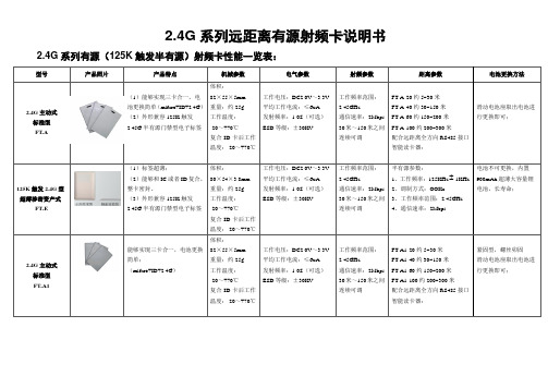
2.4G系列远距离有源射频卡说明书2.4G系列有源(125K触发半有源)射频卡性能一览表:型号产品照片产品特点机械参数电气参数射频参数距离参数电池更换方法2.4G主动式标准型FT-A (1)能够实现三卡合一,电池更换简单(mifare+ID+2.4G)(2)外形兼容125K触发2.45G半有源门禁型电子标签体积:82×55×5mm重量:约25g工作温度:-20~+70℃复合ID卡后工作温度:-20~+70℃工作电压:DC2.0V~3.3V平均工作电流:≤6uA发射频率:1.0S(可选)ESD等级:±30KV工作频率范围:2.45GHz通信速率:2Mbps30米~150米之间连续可调FT-A-20约5~30米FT-A-40约30~150米FT-A-60约150~200米FT-A-100约200~300米配合远距离全方向RS485接口智能读卡器:滑动电池座取出电池进行更换即可;125K触发2.4G型超薄涉密资产式FT-E (1)标签超薄;(2)能够和IC或者ID复合,整卡密封。
(3)外形兼容125K触发2.45G半有源门禁型电子标签体积:80×54×3.8mm重量:约25g工作温度:-20~+70℃复合ID卡后工作温度:-20~+70℃工作电压:DC2.0V~3.3V平均工作电流:≤6uA发射频率:1.0S(可选)ESD等级:±30KV工作频率范围:2.45GHz通信速率:2Mbps30米~150米之间连续可调半有源参数:1、工作频率:125KHz 1KHz2、调制方式:OOKc3、工作频率范围:2.45GHz4、通信速率:2Mbps电池不可更换,内置900mAh超薄大容量锂电池,长寿命;2.4G主动式标准型FT-A1 能够实现三卡合一,电池更换简单;(mifare+ID+2.4G)体积:82×55×5mm重量:约25g工作温度:-20~+70℃复合ID卡后工作温度:-20~+70℃工作电压:DC2.0V~3.3V平均工作电流:≤6uA发射频率:1.0S(可选)ESD等级:±30KV工作频率范围:2.45GHz通信速率:2Mbps30米~150米之间连续可调FT-A1-20约5~30米FT-A1-40约30~150米FT-A1-60约150~200米FT-A1-100约200~300米配合远距离全方向RS485接口智能读卡器:紧固型,螺丝卯固滑动电池座取出电池进行更换即可;2.4G主动式煤矿人员卡FT-M125K被动触发标签体积小,质量轻,方便粘贴在物体表面,更换电池简单1节CR2032纽扣电池体积:φ33×8.5mm重量:约18g工作温度:-20~+70℃工作电压:DC2.0V~3.3V平均工作电流:≤8uA发射频率:1.0SESD等级:±8 KV工作频率范围:2.4~2.5GHz通信速率:1Mbps配合全向读卡器:85米配合定向读卡器:在20~200米之间连续可调使用螺丝刀拆除上盖,可直接更换电池,再重新安装上外壳即可2.4G主动式钥匙扣型FT-J 外形美观,钥匙扣式挂带设计,电池更换简单1节CR2032纽扣电池体积:57.5×32×11mm重量:约26g工作温度:-20~+70℃工作电压:DC2.0V~3.3V平均工作电流:≤8uA发射频率:1.0SESD等级:±8 KV工作频率范围:2.4~2.5GHz通信速率:1Mbps配合全向读卡器:85米配合定向读卡器:在20~150米之间连续可调使用螺丝刀拆除上盖,可直接更换电池,再重新安装上外壳即可2.4G主动式按键报警型FT-B可升级为125K被动触发标签能够实现三卡合一,电池更换简单,有太阳能功能功能(mifare+ID+2.4G)与读卡器配套使用能够实现按键报警功能体积:86×55×8.0mm重量:约32g工作温度:-20~+70℃工作电压:DC2.0V~3.3V平均工作电流:≤8uA发射频率:1.0SESD等级:±8 KV工作频率范围:2.4~2.5GHz通信速率:1Mbps配合全向读卡器:85米配合定向读卡器:在20~150米之间连续可调。
G代码一览表

CNC代码一览表M代码一览表注)不能同时处理的M代码M32中虽然在1程序程序段中能加入4个M代码,但不能同时处理的M代码加入程序时,会发出“227不能同时处理的M代码”的警示.此警示的组合如下:M03﹑M04、M05、M19中的2个以上在同一程序段中M15﹑M16在同一程序段中M23﹑M24在同一程序段中M33﹑M34在同一程序段中M48﹑M49在同一程序段中M15﹑M33在同一程序段中M06﹑M149在同一程序段中M70~M72中两个以上在同一程序段中(只在带有换托盘功能中)M195~M198不能同时单独发指令不合规格的M代码当发出M代码表中没有的M代码或不合规格的M代码指令时,会提示“228不合规格的M代码”,并终止程序,这一点请注意.但是,M36~M39指令什么也不进行,便到达完了状态.G代码一览表表1.1从表中我们可以看到,G代码被分为了不同的组,这是由于大多数的G代码是模态的,所谓模态G代码,是指这些G代码不只在当前的程序段中起作用,而且在以后的程序段中一直起作用,直到程序中出现另一个同组的G代码为止,同组的模态G代码控制同一个目标但起不同的作用,它们之间是不相容的。
00组的G代码是非模态的,这些G代码只在它们所在的程序段中起作用。
标有*号的G代码是上电时的初始状态。
对于G01和G00、G90和G91上电时的初始状态由参数决定。
如果程序中出现了未列在上表中的G代码,CNC会显示10号报警。
同一程序段中可以有几个G代码出现,但当两个或两个以上的同组G代码出现时,最后出现的一个(同组的)G代码有效。
在固定循环模态下,任何一个01组的G代码都将使固定循环模态自动取消,成为G80模态。
电缆敷设方式

SR:沿钢线槽敷设BE:沿屋架或跨屋架敷设CLE:沿柱或跨柱敷设WE:沿墙面敷设CE:沿天棚面或顶棚面敷设ACE:在能进入人的吊顶内敷设BC:暗敷设在梁内CLC:暗敷设在柱内WC:暗敷设在墙内CC:暗敷设在顶棚内ACC:暗敷设在不能进入的顶棚内FC:暗敷设在地面内SCE:吊顶内敷设,要穿金属管一,导线穿管表示SC-焊接钢管MT-电线管PC-PVC塑料硬管FPC-阻燃塑料硬管CT-桥架MR-金属线槽M-钢索CP-金属软管PR-塑料线槽RC-镀锌钢管二,导线敷设方式的表示DB-直埋TC-电缆沟BC-暗敷在梁内CLC-暗敷在柱内WC-暗敷在墙内CE-沿天棚顶敷设CC-暗敷在天棚顶内SCE-吊顶内敷设F-地板及地坪下SR-沿钢索BE-沿屋架,梁WE-沿墙明敷三,灯具安装方式的表示CS-链吊DS-管吊W-墙壁安装C-吸顶R-嵌入S-支架CL-柱上沿钢线槽:SR沿屋架或跨屋架:BE沿柱或跨柱:CLE穿焊接钢管敷设:SC穿电线管敷设:MT穿硬塑料管敷设:PC穿阻燃半硬聚氯乙烯管敷设:FPC 电缆桥架敷设:CT金属线槽敷设:MR塑料线槽敷设:PR用钢索敷设:M穿聚氯乙烯塑料波纹电线管敷设:KPC穿金属软管敷设:CP直接埋设:DB电缆沟敷设:TC导线敷设部位的标注沿或跨梁(屋架)敷设:AB暗敷在梁内:BC沿或跨柱敷设:AC暗敷设在柱内:CLC沿墙面敷设:WS暗敷设在墙内:WC沿天棚或顶板面敷设:CE暗敷设在屋面或顶板内:CC吊顶内敷设:SCE地板或地面下敷设:FCHSM8-63C/3PDTQ30-32/2P 这两个应该是两种塑壳断路器的型号,HSM8-63C/3P 适用于照明回路中,为3极开关,额定电流为63A(3联开关)DTQ30-32/2P 也是塑壳断路器的一种,额定电流32A,2极开关其他那些符号都是关于导线穿管和敷设方式的一些表示方法,你对照着查一下矿用铠装控制电缆;MKVV22,MKVV32 2*0.5,3*0.75,4*4,------37*1.5mm铠装控制电缆;KVV22,KVV32,KVVR22 2*0.5,3*0.75,4*4,------37*1.5mm 铠装屏蔽控制电缆KVVP-22,RVVP-22,KVVRP-22,KVVP2-22,KVVRP2-222*0.5,3*0.75,4*4,------37*1.5mm铠装阻燃控制电缆;ZR-KVV22,ZR-KVV32,ZR-KVVR222*0.5,3*0.75,4*4,------37*1.5mm铠装阻燃屏蔽控制电缆;ZR-KVVP22,ZR-KVVRP22,ZR-KVVP2-22,ZR-KVVRP2-222*0.5,3*0.75,4*4,------37*1.5mm铠装通信电缆;HYA22,HYA23,HYA53,HYV22,HYV23 5对,10对------2400 对,0.4-0.5-0.6-0.7-0.8-0.9线径铠装充油通信电缆;HYAT22,HYAT23,NYAT53 5对,10对------800对0.4-0.5-0.6-0.7-0.8-0.9线径铠装阻燃通信电缆;ZR-HYA22,ZR-HYA23,ZR-HYA53,WDZ-HYA23,WDZ-HYA535对,10对------2400对,0.4-0.5-0.6-0.7-0.8-0.9线径矿用铠装阻燃通信电缆;MHYA22,MHYV22,MHYA32,MHYV325对,10对------200对,0.5-0.6-0.7-0.8-0.9-1.0线径铠装计算机电缆;DJYVP22,ZR-DJYVP22,DJYVRP22,DJYPV22,ZR-DJYPV22DJYPVR22 DJYPVP22,DJYPVRP22,ZR-DJYPVP22,ZR-DJYPVPR221*2*0.75 2*2*1.0 3*2*1.5 ------30*2*1.5mm铠装铁路信号电缆;PZY23,PTY23,PZY22,PTY22,PZYH23,PTYH23 PZYA23,PZYA22,PZYAH22,PTYAH22,PTYAH32,PZY324芯-6芯-8芯-9芯------6型号含义:R-连接用软电缆(电线),软结构。
APT-M803M中文说明书

ANPRO-TECH无线控制系统ANPRo-TECH REMOTE无线遥控系统-产品介绍-安装和操作手册KEHAO23B1201AJ.docMay27,2015AP目录概述 (3)发射机和接收机同步 (3)指示灯LED (5)输出 (5)输入 (5)安装 (5)上电之前 (6)使用PALM™接口 (6)诊断 (6)内部状态图形显示 (7)文件传输 (8)查找问题 (9)输出使能 (10)发射器内部线路 (10)接收机接线 (11)日常维护 (11)保养注意事项 (12)检修 (13)故障排除图示 (14)错误代码 (15)发射机外形尺寸 (16)接收机外形尺寸 (17)系统参数 (18)温馨提示 (19)详细说明参数北美无线电型号核准FCC ID:P4U-VRTS加拿大工业部认证号:4534A-VRTS设备类别:PART15SPREAD SPECTRUM TRANSMITTER发射机电源...........................................................................................Customer supplied 工作温度......................................................................................-40˚C to+85˚C 保存温度.....................................................................................-40˚C to+100˚C 射频频率...............................................................................................223-235MHz 发射功率............................................................................................................33mW 抗震频率..................................................................................................3G to200Hz 冲击............................................................................................................................50G NEMA (12)接收器电源电压........................................................................................................9-30VDC 工作温度........................................................................................-40˚C to+85˚C 保存温度.....................................................................................-40˚C to+100˚C 输出电流........................................................................5.0A max each,sourcing 数字输入(装备后).........................................................................................电源电压模拟输入.........................................................................................0-5VDC/4-20mA 射频频率...............................................................................................223-235MHz 震动..........................................................................................................3G to200Hz 冲击.........................................................................................................................100G NEMA (4X)概述APT-M803无线控制系统是一种基于微处理器的无线控制系统。
- 1、下载文档前请自行甄别文档内容的完整性,平台不提供额外的编辑、内容补充、找答案等附加服务。
- 2、"仅部分预览"的文档,不可在线预览部分如存在完整性等问题,可反馈申请退款(可完整预览的文档不适用该条件!)。
- 3、如文档侵犯您的权益,请联系客服反馈,我们会尽快为您处理(人工客服工作时间:9:00-18:30)。
Large Can Aluminum Electrolytic Capacitors
FEATURES
• NEW SIZES FOR LOW PROFILE AND HIGH DENSITY DESIGN OPTIONS • EXPANDED CV VALUE RANGE
• HIGH RIPPLE CURRENT
• LONG LIFE • CAN-TOP SAFETY VENT
• DESIGNED AS INPUT FILTER OF SMPS • STANDARD 10mm (.400") SNAP-IN SPACING NRLM Series
SPECIFICATIONS
(* 47,000µF add 0.14, 68,000µF add 0.35.)Notice for Mounting
The space from the top of the can shall be more than (3mm) from chassis or other construction materials so that safety vent has room to expand in case of emer g en c y.
Sleeve Color: Dark
Blue
Can Top Safety Vent
Insulation Sleeve and Minus Polarity Marking
(4.0mm Leads Available As Option)
D+1Max.
L ± 2
6.3 ± 10.8
10
(-)
(+)
MAXIMUM EX P AN S ION
FOR SAFETY VENT Approx. 3.0mm
Recommended PC Board Mounting Holes:
10 ± .1
∅= 2 ± 0.1
D ∅ ± 0.5
Chassis
PC Board
PRECAUTIONS
Please review the notes on correct use, safety and precautions found on pages T10 & T11
of NIC’s Electrolytic Capacitor catalog . Operating Temperature Range
-40 ~ +85°C
-25 ~ +85°C Rated Voltage Range 16 ~ 250Vdc 350 ~ 450Vdc Rated Capacitance Range 180 ~ 68,000µF
56 ~ 680µF
Capacitance Tolerance ±20% (M)Max. Leakage Current (µA)After 5 minutes (20°C)
3 x C(µF)V
Max. Tan δ
at 120Hz/20°C W.V. (Vdc)162535506380100160~450Tan δ max.
0.50*0.40*0.350.300.250.200.200.15Surge Voltage
W.V. (Vdc)162535506380100160S.V. (Vdc)
2032446379100125200W.V. (Vdc)180200250350400450--S.V. (Vdc)220250300400450500--Ripple Current
Correction Factors Frequency (Hz)50601001205001K 10K ~ 50K -Multiplier at 85°C
0.750.800.95 1.00 1.05 1.08 1.15-Low Temperature
Stability (10 to 250Vdc)
Temperature (°C)
0-25-40-----Capacitance Change
-5%-15%-30%-----Impedance Ratio 1.5
39-----Load Life Test
2,000 hours at +85°C
Capacitance Change
Within ±20% of initial measured value Tan δ
Less than 200% of specifi ed maximum value
Leakage Current Less than specifi ed maximum value Shelf Life Test
1,000 hours at +85°C (no load)Capacitance Change Within ±20% of initial measured value Tan δ
Less than 200% of specifi ed maximum value
Leakage Current Less than specifi ed maximum value Surge Voltage Test Per JIS-C-5141 (table #6, #4)Surge voltage applied: 30 seconds
"On" and 5.5 minutes no voltage "Off"
Capacitance Change Within ±20% of initial measured value Tan δLess than 200% of specifi ed maximum value
Leakage Current Less than specifi ed maximum value Soldering Effect
Refer to MIL-STD-202F Method 210A Capacitance Change Within ±10% of initial measured value
Tan δ
Less than specifi ed maximum value Leakage Current
Less than specifi ed maximum value
RoHS Compliant
includes all homogeneous materials
*See Part Number System for Details
Large Can Aluminum Electrolytic Capacitors
NRLM Series
NRLM 222 M 50V 20X25 F
RoHS compliant Case Size (mm) Voltage Rating Tolerance Code PART NUMBER SYSTEM
Large Can Aluminum Electrolytic Capacitors NRLM Series STANDARD PRODUCT LIST, CASE SIZE AND SPECIFICATIONS。