
Memory Compiler
SEC ASIC
5-1
STDL80
MEMORY COMPILERS SELECTION GUIDE
MEMORY COMPILERS
In 0.5µm CMOS standard cell memory compilers, the y-mux type selecting option was added to give the customers freedom selecting aspect ratio of the memory layout. Many of the characteristics of a memory cell are depend on its y-mux type. So, when you change the y-mux type from one to the other to change the aspect ratio, you have to know that it will change many major characteristics, such as access time, area and power consumption, of the memory. < Figure 1. Example of Y-mux Types and Aspect Ratio >
y-mux ቤተ መጻሕፍቲ ባይዱ 4
y-mux = 8
y-mux = 16
Dual Banks
In some of 0.5µm CMOS standard cell memory compilers is a generator option which defines the number of bit array banks. This dual bank scheme doubles the maximum capacity of the memory compilers.
MEMORY COMPILERS
OVERVIEW
OVERVIEW
This chapter contains information for memory compilers available in STDL80 cell library. These are complete compilers that consist of various generators to satisfy the requirements of the circuit at hand. Each of the final building block, the physical layout, will be implemented as a stand-alone, densely packed, pitch-matched array. Using this complex layout generator and adopting state-of-the-art logic and circuit design technique, these memory cells can realize extreme density and performance. In each layout generator, we added an option which makes the aspect ratio of the physical layout selectable so that the ASIC designers can choose the aspect ratio according to the convenience of the chip level layout. In the STDL80 cell library, there are 4 groups of memory compilers — ROMs; Static RAMs; Register File; FIFO.
Advanced Design Technique
All of 0.5µm CMOS standard cell memory compilers adopt very advanced design technique to obtain extremely high performance in terms of both speed and power consumption. Below are major techniques. For reducing power consumption • Minimized bit-line precharge/discharge voltage swing • Zero static current consuming sense amplifier • Automatic power down after an access For optimizing and minimizing the read access time • Size sensitive self-timer delay • Extremely simple tri-state output circuit
MEMORY COMPILERS SELECTION GUIDE
Memory Group ROM Cell Name CROM Gen DROM Gen Static RAM SPSRAM Gen SPSRAMA Gen Function Description Contact Programmable Synchronous ROM Generator Diffusion Programmable Synchronous ROM Generator Single-Port Synchronous RAM Generator – Reads and writes at the same edge of clock Single-Port Synchronous RAM Generator – Alternative – Reads and writes at different edges of clock Single-Port Asynchronous RAM Generator – Fully asynchronous read, WEN synchronized write Dual-Port Synchronous RAM Generator – Reads and writes at the same edge of clock Dual-Port Asynchronous RAM Generator – Fully asynchronous read, WEN synchronized write Dual-Port Synchronous RAM Generator – Alternative – Reads and writes at different edges of clock 1 Read Port, 1 Write Port Synchronous Register File Synchronous FIFO
Flexible Aspect Ratio
The size of a memory cell is defined by its number of words (WORDS) and number of bits per word (BPW). But, this size is only a logical size. The physical size of a memory is defined by the number of rows (ROWS) and the number of columns (COLS) of its bit cell array. Usually, we can't make the bit cell array with WORDS and BPW because the range of WORDS is much larger than the range of BPW. If we make the bit cell array with WORDS and BPW, most of memory layouts will have too tall and too thin aspect ratio. Therefore, column decoder and y-mux circuit are included in most of memory cells to adjust the aspect ratio.
Memory Compilers
5
Contents
Overview .............................................................................................................................. 5-1 Memory Compilers Selection Guide..................................................................................... 5-2 CROM Gen........................................................................................................................... 5-3 DROM Gen........................................................................................................................... 5-9 SPSRAM Gen ...................................................................................................................... 5-15 SPSRAMA Gen .................................................................................................................... 5-22 SPARAM Gen....................................................................................................................... 5-31 DPSRAM Gen ...................................................................................................................... 5-38 DPSRAMA Gen.................................................................................................................... 5-47
编译原理第四版课后答案
编译原理第四版课后答案1. What are the three basic phases of a compiler and what are their main functions?- The three basic phases of a compiler are lexical analysis, syntax analysis, and code generation.- The main function of lexical analysis is to read the source code and break it into individual tokens, such as keywords, identifiers, numbers, and symbols.- The main function of the syntax analysis is to parse the tokens and verify that they form valid syntax according to the grammar rules of the programming language.- The main function of code generation is to convert the parsed tokens into executable code in a target programming language or machine code.2. What is lexical analysis and what are its main tasks?- Lexical analysis is the first phase of a compiler, which reads the source code and breaks it into individual tokens.- The main tasks of lexical analysis include tokenization, where the source code is divided into meaningful units called tokens, such as keywords, identifiers, numbers, and symbols; removal of comments, where any comments in the source code are ignored; and removal of white spaces, where unnecessary spaces, tabs, and line breaks are eliminated.3. What is a parser and what is its main function?- A parser is a component of the compiler that performs syntax analysis, also known as parsing.- Its main function is to analyze the structure of the tokens generated by the lexical analysis phase and verify that they form avalid syntax according to the grammar rules of the programming language.- The parser constructs a derivation tree or a parse tree to represent the structure of the code and checks for syntax errors, such as missing or misplaced tokens.4. What is the difference between a compiler and an interpreter?- A compiler is a program that translates the entire source code of a programming language into an equivalent target code or machine code before execution.- An interpreter, on the other hand, does not translate the entire source code into machine code before execution. Instead, it reads and executes the source code line by line, translating and executing each line as it encounters it.- In terms of efficiency, a compiled program tends to run faster than an interpreted program because the compiled code is already in machine language, whereas the interpreted code needs to be translated and executed at runtime.5. What are the advantages and disadvantages of using an interpreted language?- Advantages of using an interpreted language include faster development time, as there is no need to compile the entire code before execution; easier debugging, as errors can be detected and fixed immediately; and platform independence, as the interpreter can run on different operating systems without the need to compile separate binaries.- Disadvantages of using an interpreted language include slower execution speed compared to compiled languages; lower performance, as the interpreter needs to translate and execute eachline at runtime; and potential security risks, as the interpreted code can be easily accessed and modified.6. What is meant by bytecode and what is its role in interpreter-based execution?- Bytecode is a low-level representation of the source code that is generated by a compiler or an interpreter. It is a set of instructions that can be executed by a virtual machine.- In interpreter-based execution, the source code is first compiled into bytecode, which is a platform-independent representation of the code. The interpreter then reads and executes the bytecode on the virtual machine, providing a compromise between compilation and interpretation.- Bytecode allows for faster execution compared to interpreting the source code directly, as the bytecode is already in a form that can be executed by the virtual machine.7. What is code optimization and why is it important?- Code optimization is the process of improving the efficiency and performance of the generated code by the compiler.- It is important because optimized code can run faster and consume less memory, resulting in improved overall performance of the program.- Code optimization techniques include constant folding, loop unrolling, dead code elimination, and register allocation, among others.8. What is a symbol table and what is its purpose?- A symbol table is a data structure that is used by a compiler to store information about the variable and function namesencountered in the source code.- Its purpose is to keep track of the properties and attributes of each symbol, such as its data type, memory location, scope, and visibility.- The symbol table is used by various phases of the compiler, such as the lexical analyzer, parser, and code generator, to perform tasks such as name resolution, type checking, and memory management.9. What is the role of an assembler in the compilation process?- An assembler is a program that converts assembly language code into machine code.- In the compilation process, the assembler is responsible for translating the assembly language code written by the programmer into machine code that can be executed directly by the computer hardware.- The assembler performs a one-to-one mapping of assembly instructions to their corresponding machine code instructions, and also resolves symbolic addresses and labels used by the programmer.10. What is the difference between a single-pass compiler and a multi-pass compiler?- A single-pass compiler is a compiler that reads the source code of a program once and generates the corresponding executable code in a single pass or iteration.- A multi-pass compiler, on the other hand, requires multiple passes or iterations over the source code in order to generate the executable code.- Single-pass compilers are generally simpler and require less memory, but they are unable to perform certain optimizations orglobal analysis that requires information from the entire source code. Multi-pass compilers are more powerful and can perform more complex optimizations and analysis, but they are typically slower and require more memory.。
synopsys iC Compiler II 数据手册说明书

DATASHEETOverview IC Compiler™ II is the industry leading place and route solution that delivers best-in-class quality-of-results (QoR) for next-generation designs across all market verticals and process technologies while enabling unprecedented productivity. IC Compiler II includes innovative for flat and hierarchical design planning, early design exploration, congestion aware placement and optimization, clock tree synthesis, advanced node routing convergence, manufacturing compliance, and signoff closure.IC Compiler II is specifically architected to address aggressive performance, power, area (PPA), and time-to-market pressures of leading-edge designs. Key technologies include a pervasively parallel optimization framework, multi-objective global placement, routing driven placement optimization, full flow Arc based concurrent clock and data optimization, total power optimization, multi-pattern and FinFET aware flow and machine learning (ML) driven optimization for fast and predictive design closure. Advanced Fusion technologies offer signoff IR drop driven optimization, PrimeTime ® delay calculation within IC Compiler II, exhaustive path-based analysis (PBA) and signoff ECO within place and route for unmatched QoR and design convergence. F U S I O N D E S I G N P L A T F O R M PrimeTime, StarRC, PrimePower,IC Validator, RedHawk Analysis Fusion Fusion Compiler IC Compiler II Design Compiler NXT TestMAX F o r m a l i t y ECO Fusion S i g n o f f F u s i o n S i g n o f f F u s i o n Test Fusion Figure 1: IC Compiler II Anchor in Synopsys Design PlatformAccelerating DesignClosure on AdvancedDesignsIC Compiler II Industry Leading Place and Route SystemKey BenefitsProductivity• The highest capacity solution that supports 500M+ instances with a scalable and compact data model• A full suite of design planning features including transparent hierarchical optimization• Out-of-the-box simple reference methodology for easy setup• Multi-threaded and distributed computing for all major flow steps• Golden signoff accuracy with direct access to PrimeTime delay calculationPPA• Unified TNS driven optimization framework• Congestion, timing, and power-driven logic re-synthesis• IEEE 1801 UPF/multi-voltage support• Arc-based concurrent clock and data optimization• Global minima driven total power optimizationAdvanced Nodes• Multi-pattern and FinFET aware design flow• Next generation advanced 2D placement and legalization• Routing layer driven optimization, auto NDR, and via pillar optimization• Machine learning driven congestion prediction and DRC closure• Highest level of foundry support and certification for advanced process nodes• IC Validator in the loop signoff driven DRC validation and fixingAdvanced Fusion Technology• Physically aware logic re-synthesis• IR drop driven optimization during all major flow steps• PrimeTime delay calculation based routing optimization for golden accuracy• Integrated PrimeTime ECO flow during routing optimization for fastest turnaround timeEmpowering Design Across Diversified ApplicationsThe dizzying pace of innovation and highly diversified applications across the design spectrum is forcing a complete rethink of the place and route systems to design and implement differentiated designs in a highly competitive semiconductor market on schedule. Designers on emerging process nodes must meet aggressive PPA and productivity goals. It essentially means efficient and intelligent handling of 100s of millions of place-able instances, multiple levels of hierarchy, 1000s of hard macros, 100s of clocks, wide busses, and 10s of modes and corners power domains and complex design constraints and process technology mandates. Emphasis on Designer ProductivityIC Compiler II is architected from the ground up for speed and scalability. Its hierarchical data model consumes 2-3X less memory than conventional tools, boosting the limits of capacity to 500M placeable instances and beyond. Adaptive abstraction and on-the-fly data management minimize memory requirements and enable fast responsive data manipulation. Near-linear multi-core threading of key infrastructural components and core algorithms such as database access and timing analysis speed up optimization at all phases of design. Patented, lossless compact modeling and independent R and C extraction allow handling more modes and corners (MCMM scenarios) with minimal runtime impact.IC Compiler II has built-in Reference Methodology(RM) that ensures fast flow bring up. This RM Flow is Foundry Process/Design Type specific to ensure a robust starting point and seamless bring up. IC Compiler II has direct access to the Golden PrimeTime delay calculation engine to minimize ECO iterations.IC Compiler II’s new data model enables designers to perform fast exploration and floorplanning with complex layout requirements. IC Compiler II can create bus structures, handle designs with n-levels of physical hierarchy, and support Multiply Instantiated Blocks (MIBs) in addition to global route driven pin assignment/feedthrough flow, timing driven macro placement, MV area design planning.A design data mismatch inferencing engine analyzes the quality of inputs and drives construct creation on the fly, delivering design insights even with “incomplete” data early in the design cycle. Concurrent traversal of logical and physical data models enables hierarchical Data-Flow Analysis (DFA) and fast interactive analysis through multi-level design hierarchies and MIBs. Data flow and feedthrough paths highlighted in Figure 2 allow analysis and manipulation through n-levels of hierarchy to complete early design exploration and prototyping.Figure 2: Fast interactive analysis through multiple-levels of physical hierarchy and MIBPipeline-register-planning shown in Figure 3, provides guidance for optimal placement to meet the stringent timing requirementsof high-performance designs. Interactive route editor integrated which is advanced node aware shown in Figure 4, allows intricate editing and routing functions, including the creation of special signal routes, buses, etc.Figure 3: Pipeline register placement enables superior QoR for designs with complex busesAchieving Best Performance, Power, Area, and TATIC Compiler II features a new optimization framework built on global analytics. This Unified TNS Driven Optimization framework is shared with Design Compiler NXT synthesis to enable physically-aware synthesis, layer assignment, and route-based optimization for improved PPA and TAT. Multi-Corner Multi-Mode (MCMM) and Multi-Voltage (MV) aware, level-based analytical algorithms continuously optimize using parallel heuristic algorithms. Multi-factor costing functions deliver faster results on both broad and targeted design goals. Concurrent PPA driven logic remapping, rewiring, and legalization interleaved with placement minimizes congested logic, resulting in simple localized logic cones that maximize routability and QoR.IC Compiler II minimizes leakage with fast and efficient cell-by-cell power selection across HVT, SVT and LVT cells and varying channel lengths. Activity-driven power optimization uses VCD/ SAIF, net toggle rates, or probability functions to drive placement decisions and minimize pin capacitances. Multi-bit register banking optimizes clock tree structures, reduces area, and net length, while automatically managing clock, data, and scan chain connections.Advanced modeling of congestion across all layers highlighted in Figure 4 provides accurate feedback throughput the flow from design planning to post- route optimization.Figure 4: Intelligent and accurate analysis for congestion and powerIC Compiler II introduces a new Concurrent Clock and Data (CCD) analysis and optimization engine that is built-in to every flow step resulting in meeting both aggressive performance and minimizing total power footprint. ARC-based CCD optimization performs clock tree traversal across all modes/corners in path-based fashion to ensure optimal delay budgeting.Robust support for clock distribution enables virtually any clock style, including mesh, multi-source, or H-tree topologies. Advanced analysis and debugging features perform accurate clock QoR analysis and debugging as highlighted in Figure 5.Figure 5: Accurate clock QoR analysis and debugging (a & b) Abstracted clock graph and schematic.(c) Latency clock graph. (d) Colored clock tree in layout.IC Compiler II features many innovative technologies that make it the ideal choice for high-performance, energy-efficient Arm®processor core implementation, resulting in industry-best milliwatts/megahertz (mW/MHz) for mobile and other applications across the board. Synopsys and Arm work closely together to offer optimized implementation of popular Arm cores for IC Compiler II,with reference flows available for Arm Cortex®-A high-performance processors and Mali GPUs. In addition, Arm offers off-the-shelf Artisan® standard cell and memory models that have been optimally tuned and tested for fast deployment in an IC Compiler II environment. Continuous technology innovation and close collaboration makes IC Compiler II the leading choice for Arm-based high- performance design.Highest Level of Advanced Node Certification and SupportIC Compiler II provides advanced node design enablement across major foundries and technology nodes—including 16/14nm,12/10nm, 7/5nm, and sub-5nm geometries. Zroute digital router technology ensures early and full compliance with the latest design rules required for these advanced node technologies. Synopsys collaborates closely with all the leading foundries to ensure that IC Compiler II is the first to deliver support for early prototype design rules and support for the final production design rules. IC Compiler II design technologies maximize the benefits of new process technologies and offer optimal return on investment for cutting-edge silicon applications.IC Compiler II advanced node design support includes multi-pattern/FinFET aware placement and routing, Next-generation advanced 2D placement and legalization, routing layer driven optimization, auto NDR, and via pillar optimization. IC Validator in the loop provides signoff DRC feedback during Implementation.Foundry fill Track based fillFigure 6: IC Validator In-Design metal fill color aware metal fill, optimized for density and foundry requirementsMachine learning driven congestion prediction and DRC closure allow for fastest routing convergence with best PPA. Multiple sets of training data are used to extract key predictive elements that guide the pre-route flow.Advanced Fusion TechnologyThe Fusion Design Platform™ delivers unprecedented full-flow QoR and time-to-results (TTR) to accelerate the next wave of semiconductor industry innovation. The industry’s first AI-enhanced, cloud-ready Design Platform with Fusion Technology™ isbuilt from Synopsys’ market-leading, massively-parallel digital design tools, and augmented with innovative capabilities to tacklethe escalating challenges in cloud computing, automotive, mobile, and IoT market segments and accelerate the next wave of industry innovation.Fusion Technology redefines conventional EDA tool boundaries across synthesis, place-and-route, and signoff, sharing integrated engines across the industry’s premier digital design products. It enables designers to accelerate the delivery of their next-generation designs with the industry-best QoR and the TTR.©2019 Synopsys, Inc. All rights reserved. Synopsys is a trademark of Synopsys, Inc. in the United States and other countries. A list of Synopsys trademarks isavailable at /copyright.html . All other names mentioned herein are trademarks or registered trademarks of their respective owners.。
Memory-Compiler使用入门介绍
Memory Compiler使用介绍在使用Memory Compiler时,请务必确保你的RAM从头到尾的规格与设定都相同,否则会造成一些不可避免的错误。
首先在RTL代码阶段,要用到RAM就要用Artisan公司提供的Memory Compile产生的verilog代码,此时不需要着急产生其他后阶段的必要数据,因为RTL代码阶段,只需要行为级模型即可。
当进入门级代码后,RAM compiler就要产生其他的相关数据了,同时要考虑RAM版图的位置与方向。
由于一个大的设计不会设计一次就会完成,所以有两个重点,第一个是每次使用RAM compiler时都一定要让它产生特性设置文档,避免忘记自己做过的设定。
第二件事是对应的文件名要定义好,否则RAM的方向不同但是又用到了相同的文件名,就会把原始数据覆盖掉。
下图为SRAM在流程中需要产生的文档RTL阶段在RTL阶段主要只是产生verilog行为级和设置文件。
因为在RTL阶段不需要考虑RAM 的位置信息。
Memory Compiler提供4种选择,分别为ra1sh,ra2sh,rf1sh,rf2sh。
前面的ra与rf分别指的是SRAM与register file,其中rf在同样的情况下比ra占的面积小,但是rf的大小有限制,其限制大小位4096bits。
而后面1sh与2sh表示位单端口还是双端口,如果SRAM 的容量比较大的话,相同设置下,1sh比2sh面积要小,速度也要快,功耗要低。
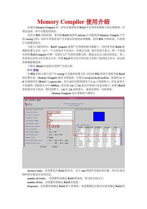
Memory Compiler运行界面如下图所示instance name:该设置是对RAM的命名,由于ram的特性有地址和位数,所以在命名的时候尽量包含这些信息。
number of words:该设置用来确定RAM的深度,即寻址空间大小。
number of bits:该设置用来确定RAM的宽度。
frequency:该设置用来确定RAM的工作频率,该设置确定后就可以基本确定RAM的功耗,估计的结果位平均电流,通过该数据来设定电源环的宽度。
主板上的英文字母都代表什么

1.主板上的英文字母都代表什么1.L----电感.电感线圈2.C----电容.3.BC---贴片电容4.R----电阻5.9231 芯片-----脉宽6.74 门电路-----它在主板南桥旁边7.PQ----场效应管8.VT、Q、V----三级管9.VD、D---二级管10.RN----排阻11. ZD----稳压二极管12.W-----电位器13.IC---稳压块14.IC、N、U----集成电路15.X、Y、G、Z----晶振16.S-----开关17.CM----频率发生器(一般在晶振14.31818 旁边)2. 计算机开机原理开机原理:插上ATX 电源后,有一个静态5V电压送到南桥,为南桥里面的ATX 开机电路提供工作条件(ATX 电源的开机电路是集成南桥里面的),南桥里面的ATX 开机电路将开始工作,会送一个电压给晶体,晶体起振工作,产生振荡,发出波形。
同时ATX 开机电路会送出一个开机电压到主板的开机针帽的一个脚,针帽的另一个脚接地。
当打开开机开关时,开机针帽的两个脚接通,而使南桥送出开机电压对地短路,拉低南桥送出的开机电压,而使南桥里的开机电路导通,拉低静态5V电压,使其变为0 电位。
使电源开始工作,从而达到开机目的。
(ATX 电源里还有一个稳压部分,它需要静态5V变为0 电位才能工作)。
3. 主板时钟电路工作原理时钟电路工作原理:3.5 电源经过二极管和电感进入分频器后,分频器开始工作,和晶体一起产生振荡,在晶体的两脚均可以看到波形。
晶体的两脚之间的阻值在450---700 欧之间。
在它的两脚各有1V左右的电压,由分频器提供。
晶体两脚常生的频率总和是14.318M。
总频(OSC)在分频器出来后送到PCI槽的B16 脚和ISA的B30 脚。
这两脚叫OSC测试脚。
也有的还送到南桥,目的是使南桥的频率更加稳定。
在总频OSC 线上还电容。
总频线的对地阻值在450---700 欧之间,总频时钟波形幅度一定要大于2V 电平。
Memory Compiler使用介绍

Memory Compiler使用介绍在使用Memory Compiler时,请务必确保你的RAM从头到位的规格与设定都相同,否则会造成一些不可避免的错误。
首先在RTL代码阶段,要用到RAM就要用Artisan公司提供的Memory Compile产生的verilog代码,此时不需要着急产生其他后阶段的必要数据,因为RTL代码阶段只需要行为级模型即可。
当进入门级代码后,RAM compiler就要产生其他的相关数据了,同时要考虑RAM版图的位置与方向。
由于一个大的设计不会设计一次就会完成,所以有两个重点,第一个是每次使用RAM compiler时都一定要让它产生特性设置文档,避免忘记自己做过的设定。
第二件事是对应的文件名要定义好,否则RAM的方向不同但是又用到了相同的文件名,就会把原始数据覆盖掉。
下图为SRAM在流程中需要产生的文档RTL阶段在RTL阶段主要只是产生verilog行为级和设置文件。
因为在RTL阶段不需要考虑RAM的位置信息。
Memory Compiler提供4种选择,分别为ra1sh,ra2sh,rf1sh,rf2sh。
前面的ra与rf分别指的是SRAM与registerfile,其中rf在同样的情况下比ra占的面积小,但是rf的大小有限制,其限制大小位4096bits。
而后面1sh与2sh表示位单端口还是双端口,如果SRAM的容量比较大的话,相同设置下,1sh比2sh面积要小,速度也要快,功耗要低。
Memory Compiler运行界面如下图所示instance name:该设置是对RAM的命名,由于ram的特性有地址和位数,所以在命名的时候尽量包含这些信息。
number of words:该设置用来确定RAM的深度,即寻址空间大小。
number of bits:该设置用来确定RAM的宽度。
frequency:该设置用来确定RAM的工作频率,该设置确定后就可以基本确定RAM的功耗,估计的结果位平均电流,通过该数据来设定电源环的宽度。
嵌入式英语词汇表

Monitor
临视器
Multiprocessing
多处理
Multitasking
多任务
Object file
目标文件
Operating system
操作系统
Parallel processing
并行进程
Peripheral
交叉编译器
Compiler
编译器
bootable disk
引导盘
boot failure
引导失败
optical disk
光碟[盘] (同compact disk)
terminal
终端
portable
可移植
library
(程序)库,库
share
共享
remote access
远程访问
localhost
本(主)机
DDR SDRAM
上升延和下降延都可以进行数据传输
LCD
Liquid Crystal Display (液晶显示器)简称
GPIO
(General Purpose Input Output)通用输入输出。
Output
输出
Input
输入
Keypad
小键盘
RTC
可提供时间(通常也提供日期)的时钟器件.
RAM
双的,双重的;
Void
空的,空虚的;没有…的;无效的
typedef
类型定义
struct
结构(上)的,构架(上)的
union
联盟
enum
枚举
define
定义
sizeof
...的大小
func
函数,功能(=function)
嵌入式系统常用英文词汇
D
DMA(直接内存访问)
Direct Memory Access. A technique for transferring data directly between two peripherals (usually memory and an I/O device) with only minimal intervention by the processor. DMA transfers are managed by a third peripheral called a DMA controller.
用来描述一个特定的嵌入式项目中的某一软件模块。应用软件不象可重用的交叉嵌入式平台,只是因为每一个嵌入式系统有不同的应用软件。
assembler(汇编编译器)
A software development tool that translates human-readable assembly languageprograms into machine-language instructions that the processor can understandand execute.
一种特殊版本的处理器,它有一些,内部的信号能传达到外置的针脚上。一个外合处理器绝大多数情况下只用在模拟器上,从来不会被特意用在产品系统上。
Breakpoint (断点)
A location in a program at which execution is to be stopped and control of the processor switched to the debugger. Mechanisms for creating and removing breakpoints are provided by most debugging tools.
DELL服务器错误代码汇总
RPM Fan Mod #C
Low
Same as above except for fan C of module #.
Fan RPM reading returns to a point inside of the intended operating range.
Yes
Any
E1311
RPM Fan Mod #B
Low
Same as above except for fan B of module #.
Fan RPM reading returns to a point inside of the intended operating range.
Yes
Any
Yes
Pre-Post
E1A11
PCIRsrConfig
High
PCI risers are not configured correctly; some invalid configurations prevent system power on.
Failing device is reseated/replaced/repaired.
High
1.8 VV voltage regulator has failed.
AC Cycle or SEL clear
Yes
Any
E1216
3.3VPwrGd
High
3.3 V voltage regulator has failed.
AC Cycle or SEL clear
Yes
Any
E1217
Failing device is reseated/replaced/repaired.
Memory-Compiler使用入门介绍
Memory Compiler使用介绍在使用Memory Compiler时,请务必确保你的RAM从头到尾的规格与设定都相同,否则会造成一些不可避免的错误。
首先在RTL代码阶段,要用到RAM就要用Artisan公司提供的Memory Compile产生的verilog代码,此时不需要着急产生其他后阶段的必要数据,因为RTL代码阶段,只需要行为级模型即可。
当进入门级代码后,RAM compiler就要产生其他的相关数据了,同时要考虑RAM版图的位置与方向。
由于一个大的设计不会设计一次就会完成,所以有两个重点,第一个是每次使用RAM compiler时都一定要让它产生特性设置文档,避免忘记自己做过的设定。
第二件事是对应的文件名要定义好,否则RAM的方向不同但是又用到了相同的文件名,就会把原始数据覆盖掉。
下图为SRAM在流程中需要产生的文档RTL阶段在RTL阶段主要只是产生verilog行为级和设置文件。
因为在RTL阶段不需要考虑RAM 的位置信息。
Memory Compiler提供4种选择,分别为ra1sh,ra2sh,rf1sh,rf2sh。
前面的ra与rf分别指的是SRAM与register file,其中rf在同样的情况下比ra占的面积小,但是rf的大小有限制,其限制大小位4096bits。
而后面1sh与2sh表示位单端口还是双端口,如果SRAM 的容量比较大的话,相同设置下,1sh比2sh面积要小,速度也要快,功耗要低。
Memory Compiler运行界面如下图所示instance name:该设置是对RAM的命名,由于ram的特性有地址和位数,所以在命名的时候尽量包含这些信息。
number of words:该设置用来确定RAM的深度,即寻址空间大小。
number of bits:该设置用来确定RAM的宽度。
frequency:该设置用来确定RAM的工作频率,该设置确定后就可以基本确定RAM的功耗,估计的结果位平均电流,通过该数据来设定电源环的宽度。
Synopsys STAR Memory System 测试、修复和诊断解决方案说明书
SYNOPSYS IP DATASHEET/ip The Synopsys Self-Test and Repair (STAR) Memory System™ is a comprehensive, integrated test, repair and diagnostics solution that supports repairable or nonrepairable embedded memories across any foundry, process node or memory IP vendor. Silicon-proven in over a billion chips on a range of process nodes, the STAR Memory System is a cost-effective solution for improving test quality and repair of manufacturing faults found in advanced technologies like FinFET. The STAR Memory System’s highly automated design implementation and diagnostic flow enables SoC designers to achieve quick design closure and significantly improve time-to-market and time-to-yield in volume production. The STAR Memory System has been certified for the ISO 26262 automotive functional safety standard by SGS-TUV Saar GmbH, an independent accredited assessor. In addition, the test and repair support for e-flash and embedded MRAM (eMRAM) enables the STAR Memory System to be used in IoT applications.SoC designers, silicon aggregators, and leading foundries targeting automotive, IoT, enterprise, and consumer applications license STAR Memory System with the added flexibility of consulting services for memory BIST planning, generation, insertion, and verification.STAR Memory System Yield Accelertor Figure 1: Synopsys STAR Memory System SolutionHighlights• Complete memory test, repair anddiagnostics solution supportingembedded SRAM, register files, CPU andGPU caches, CAM, multi ports, embeddedflash, MRAM as well as external memorysuch as DDR/LPDDR• Increased design productivity withhierarchical architecture and automatedsystem-on-chip (SoC) integration andverification• High-quality test to provide full memorydefect coverage with minimum test time• High yield with efficient on-chip repairacross multiple operating corners• Superior diagnostics with physical failedbitmaps and XY coordinate identificationto quickly determine root cause of failures• Increased field reliability with STARMemory System Compiler for ErrorCorrecting Codes’ (ECC) multi-bit transienterror correction• ISO 26262 certified to meet the safetyrequirements of high reliability designstargeting up to and including the moststringent ASIL D standard• Supports Internet of Things (IoT)applications with the industry’s firstcommercial built-in self-test (BIST)solution for embedded flash andembedded MRAM (eMRAM)STAR Memory System SolutionFigure 2: The Synopsys STAR Memory System helps save millions of dollars in recovered silicon,reduces test costs, and shortens time-to-volumeThe STAR Memory System Solution Consists of:• Synthesizable test and repair register transfer level (RTL) IP• STAR Memory System Design Acceleration (DA) scripts: Automates the planning, generation, insertion, and verification of test and repair RTL IP• STAR Memory System Yield Accelerator: Automates the generation of tester ready patterns in WGL/STIL/SVF, test algorithm programmability and post silicon failure diagnostics and fault classification• STAR Memory System Silicon Browser: Provides interactive silicon debug of memory using a personal computer or workstation • STAR Memory System ECC: Automatically generates ECC Verilog code, testbenches and scripts for single-port and multiport SRAM memories• STAR Memory System ext-RAM: Offers a high-coverage, cost-effective test with optional Post Package Repair (PPR) and diagnostics solution for external memories such as DDR, LPDDR and HBM via JTAG, either during production or in-field test • STAR Memory System CAM: Supports specialty content addressable memory (CAM) such as binary, ternary and XYCAMs with support for common CAM capabilities• STAR Memory System eMRAM: Optimizes manufacturing yield for eMRAM technology with inclusion of NVM specific test algorithms and support for trimming in addition to test, repair and diagnosisFlexible, Open SystemTo provide STAR Memory System access to all memory developers, Synopsys offers a specialized memory description language called MASIS. The MASIS language, together with a MASIS compiler, simplifies and automates the process of creating and verifying memory views used by the STAR Memory System. By providing an open interface to the STAR Memory System, Synopsys extends the value of the system to all users regardless of whether or not they elect to use Synopsys memories (Figure 2).High-Performance Core SupportThe STAR Memory System allows at-speed test and repair of high-performance processor cores by using a preconfigured test bus, which provides access to the memories inside the core in test mode. The STAR Memory System uses this shared Multi-Memory Bus (MMB) to test memories and add memory test and repair logic outside the IP core to avoid any impact on processor core performance (Figure 1).Test Algorithm ProgrammabilityThe STAR Memory System provides full test algorithm programmability. The STAR Memory System processor includes a BIST module to execute test algorithms. The default test algorithms in the BIST module can be replaced with new algorithms in the RTL or in silicon, and the user can program either their own custom algorithms or select from the comprehensive library of algorithms provided in the STAR Memory System.2Tester Patterns and DiagnosticsThe STAR Memory System Yield Accelerator addresses the need to identify, analyze, isolate and classify memory faults as designs are readied for transition from first silicon to volume manufacturing rapidly, cost-effectively and accurately. Leveraging the infrastructure of the STAR Memory System, the Yield Accelerator automatically generates vectors for test equipment and provides fault analysis and root-cause failure guidance based on silicon test results. Using this feature, test and product engineers can rapidly analyze failures manifested in embedded memories and inspect the physical location and class of each fault to determine the root cause without involving the IP vendor or SoC designer.On-Chip Self-RepairUnlike complex external repair flows, the STAR Memory System’s on-chip repair is fully automated. A built-in self-diagnosis module determines the location of any memory defect and provides error logging by scanning out failure data for silicon debug. When testing memories with redundancies that have failures, a built-in repair and redundancy allocation module identifies available redundant elements and determines the best possible redundancy configuration.Integrated Test and Repair with Synopsys Embedded MemoriesBy hardening the timing-critical test and repair logic within the memory hard macro, the Synopsys STAR Memory System provides unique integration with Synopsys Embedded Memory Compilers. Optimal placement of the timing-critical test and repair logic near the memory allows faster design closure, higher performance, better area and reduced power.Silicon Bring-up and CharacterizationThe STAR Memory System Silicon Browser has advanced automation capabilities to interactively communicate through a JTAG port with the STAR Memory System’s infrastructure in a chip for post-silicon bring-up, system debug, diagnosis and characterization of embedded memories. The unique features of the Silicon Browser allow full extraction of memory contents, multi-corner and multi-voltage characterization, precise physical failure localization, defect classification and redundancy utilization analysis, all from an engineer’s desktop, and without the need for expensive automatic test equipment.©2023 Synopsys, Inc. All rights reserved. Synopsys is a trademark of Synopsys, Inc. in the United States and other countries. A list of Synopsys trademarks isavailable at /copyright.html. All other names mentioned herein are trademarks or registered trademarks of their respective owners.02/27/23.CS1057939197-Update-to-STAR-Memory-System-DS.。