TLP701场管输出光藕
acplm50l 原理 -回复

acplm50l 原理-回复ACPLM50L 原理ACPLM50L是一种广泛应用于工业领域的光电隔离器件,其原理是基于光电耦合器(Optocoupler)的工作原理。
光电耦合器是一种能够将输入端的电信号转换成光信号,并通过光耦合器中的光电二极管将光信号转换成输出端的电信号的器件。
ACPLM50L主要由光电二极管(Photodiode)、光电晶体管(Phototransistor)和输出控制电路组成。
光电二极管负责将输入电信号转换成光信号,光电晶体管负责将光信号转换成输出电信号,输出控制电路则用于控制输出电路的开关状态。
在ACPLM50L中,光电二极管被放置在输入端,其内部由PN结构组成,当输入信号电压施加在PN结上时,PN结会产生电场,电场会改变PN 结内的载流子浓度,从而影响载流子的流动。
当载流子流动时,光电二极管的阴阳极之间会产生压差,导致光电二极管产生正面的制动电压,并在其连结端产生光信号。
接着,光信号通过光电晶体管中的光电二极管转换成电信号。
光电晶体管中的光电二极管和晶体管是通过共用一体结构实现的,当光信号照射到光电二极管时,光电二极管会产生正电荷。
正电荷被送到晶体管的基极,从而使晶体管的电流变化,最后通过输出接口输出。
在ACPLM50L中,输出控制电路用于控制输出端的开关状态。
输出控制电路通过对光电晶体管的驱动,来控制输出电路的开闭。
当输入信号的电压高于设定阈值时,输出电路开启,输出端产生正常的电信号;当输入信号的电压低于设定阈值时,输出电路关闭,输出端不产生电信号。
输出控制电路的设计能够提供有效的电隔离效果,使得输入端和输出端之间的电信号相互隔离,从而有效地防止干扰。
ACPLM50L具有高精度、高速度和高可靠性的特点,被广泛应用于各种测量、控制和通信系统中。
其原理简单易懂,并且具有较强的抗干扰能力,能够有效保护输入和输出端的电路。
另外,ACPLM50L还具有小尺寸、低功耗和长寿命等优点,使其成为工业领域中不可或缺的元件。
厦门华联电子股份有限公司 HPC357× 光敏晶体管输出型光耦合器 产品规格书说明书
产品规格书SPECIFICATION产品名称:光敏晶体管输出型光耦合器DESCRIPTION:Photo-transistor Output Opto-coupler产品型号:HPC357×PART NO.:HPC357×电话Tel :86-0592-*******传真Fax :86-0592-*******网址Web :地址:厦门市翔安区舫阳南路189号Add :No.189,Fangyang South Road,Xiangan District,Xiamen China.拟制Prepared 审核Verified 批准Approved厦门华联电子股份有限公司Xiamen Hualian Electronics Corp.,Ltd.1概述GeneralHPC357×是光敏晶体管输出型光耦合器,将红外LED芯片和光敏晶体管芯片封装在一起,以实现电一光一电转换。
The HPC357×is Photo-transistor Output Opto-coupler,that infrared LED chip andPhoto-transistor chip are assembled on lead frame,in order to change theelectricity-light-electricity.图1产品Figure1-Product 2特点Features●光敏晶体管输出Phototransistor output●输入、输出端之间绝缘电压高Isolation voltage between input and output VISO≥3750Vrms●双列贴片式4L塑料封装SOP4L Plastic Package●UL安全认证Safety certification of UL●VDE安全认证Safety certification of VDE●符合RoHS指令最新要求及REACH法规最新要求。
光耦反馈常见几种连接方式及其工作原理

光耦反馈常见几种连接方式及其工作原理来源:互联网•作者:佚名• 2017-11-07 14:12 • 23793次阅读在一般的隔离电源中,光耦隔离反馈是一种简单、低成本的方式。
但对于光耦反馈的各种连接方式及其区别,目前尚未见到比较深入的研究。
而且在很多场合下,由于对光耦的工作原理理解不够深入,光耦接法混乱,往往导致电路不能正常工作。
本研究将详细分析光耦工作原理,并针对光耦反馈的几种典型接法加以对比研究。
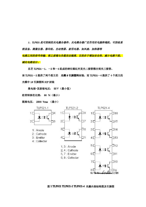
1、常见的几种连接方式及其工作原理常用于反馈的光耦型号有TLP521、PC817等。
这里以TLP521为例,介绍这类光耦的特性。
TLP521的原边相当于一个发光二极管,原边电流If越大,光强越强,副边三极管的电流Ic越大。
副边三极管电流Ic与原边二极管电流If的比值称为光耦的电流放大系数,该系数随温度变化而变化,且受温度影响较大。
作反馈用的光耦正是利用“原边电流变化将导致副边电流变化”来实现反馈,因此在环境温度变化剧烈的场合,由于放大系数的温漂比较大,应尽量不通过光耦实现反馈。
此外,使用这类光耦必须注意设计外围参数,使其工作在比较宽的线性带内,否则电路对运行参数的敏感度太强,不利于电路的稳定工作。
通常选择TL431结合TLP521进行反馈。
这时,TL431的工作原理相当于一个内部基准为2.5V的电压误差放大器,所以在其1脚与3脚之间,要接补偿网络。
常见的光耦反馈第1种接法,如图1所示。
图中,Vo为输出电压,Vd为芯片的供电电压。
com信号接芯片的误差放大器输出脚,或者把PWM芯片(如UC3525)的内部电压误差放大器接成同相放大器形式,com信号则接到其对应的同相端引脚。
注意左边的地为输出电压地,右边的地为芯片供电电压地,两者之间用光耦隔离。
图1所示接法的工作原理如下:当输出电压升高时,TL431的1脚(相当于电压误差放大器的反向输入端)电压上升,3脚(相当于电压误差放大器的输出脚)电压下降,光耦TLP521的原边电流If增大,光耦的另一端输出电流Ic增大,电阻R4上的电压降增大,com引脚电压下降,占空比减小,输出电压减小;反之,当输出电压降低时,调节过程类似。
PP701
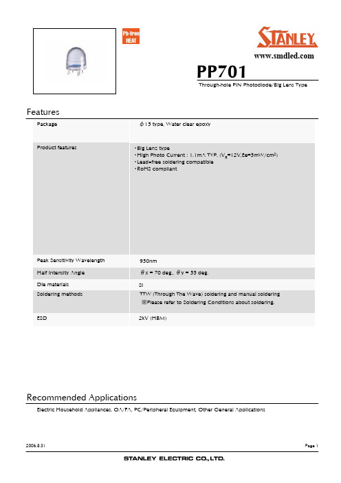
Pre-heating
100 ℃ (MAX.) Resin surface temperature
Solder Bath Temp.
265 ℃ (MAX.)
Dipping Time
5s
(MAX.)
Position
At least 3.0 mm away from the root of lead
1) The dip soldering process shall be twice maximum.
2kV (HBM)
Recommended Applications
Electric Household Appliances, OA/FA, PC/Peripheral Equipment, Other General Applications
2006.8.31
Page 1
洸子其科技是一家从事发光二极管产品研发、生产及销售公司, 致力于为国内国际市场提供高品质,低成本的各类发光管。
Dark Current Cosmetic Appearance
EE Value of each product
※The detail is described to LED and Photodetector handling precautions of home page: "Mounting through-hole Type Devices“ and "Soldering", and use it after the confirmation, please.
Testing Conditions
EIAJ ED4701/100(101)
EIAJ ED4701/300(302)
PS2801-1,TLP181,TLP121,FODM121,SFH690T迷你封装晶体管输出光耦参数应用原理

PS2801-1,TLP181,TLP121,FODM121,SFH690型号库存产商封装包装PS2801-1 77130 Toshiba SOP-4 3K/REELTLP181 95000 Toshiba SOP-4 3K/REELTLP121 77130 Toshiba SOP-4 3K/REEL FODM121 25000 Fairchild SOP-6 2.5K/REEL SFH690 17000 Vishay SOP-4 2K/REEL这几款是采用Mini型封装的晶体管输出光电耦合器,TLP181,TLP121,FODM121,SFH690采用的是SOP封装,PS2801-1采用的则是更小的SSOP封装。
SSOP SOP他们与普通4 PIN DIP封装的PC817,TLP521一样,采用红外线LED+光敏三极体的形式实现基本的隔离功能,因此,在隔离需求不是特别高达到四、五千伏的情况下,这些采用SSOP,SOP封装的光耦是可以完全替代PC817,LP521等DIP封装光耦的,因为他们的功能是完全一样的。
相比之下,他们采用的Mini型封装具有自己的优势,SOP相比DIP能节省42%的PCB面积,而SSOP相比DIP更是能节省近60%的PCB面积,为客户在成本与设计上提供能更大的空间。
基本参数PS2801-1 TLP121 TLP181 FODM121 SFH690封装SSOP SOP SOP SOP SOP隔离电压BVs 2500 Vrms 3750 Vrms 3750 Vrms 3750 Vrms 3750 Vrms崩溃电压BVce 80 V 80 V 80 V 80V 80 V需要注意的是,晶体管输出光耦一般属于线性光耦,但是其电流传输比(CTR)随输入电流的变化是很大的,而厂商给出的CTR值一般是在IF=5mA,VCE=5V的条件下的测试值,而根据下面CTR与IF的曲线,为了保证CTR的波动不会太大,建议IF在5-15mA的范围内。
TLP521-4中文资料(光电耦合器 电流不大)
Rank GB 100
600
Blank, GR, BL, GB GR, BL, GB
*1: Ex. rank GB: TLP521−1 (GB)
(Note): Application type name for certification test, please use standard product type name,
2500vrms最小1tlp521tlp5212tlp52141tlp521tlp5212tlp5214图11ttllpp552211ttllpp55221122ttllpp55221144光藕内部结构图及引脚图2tlp52122tlp5212图22ttllpp55221122光电耦合器引脚排列图absolutemaximumratingsta25absolutemaximumratingsta25aabbssoolluutteemmaaxxiimmuummrraattiinnggss绝对最大额定值ttaa2255rating数值symbolunicharacteristic参数符号?t单位?tlp521??2??tlp521??1??tlp521??4forwardcurrent正向电流if7050ma????forwardcurrentif??093ta??05ta25maderating正向电流减率50ledpulseforwardcurrent瞬间ifp1100pulse100ppsa正向脉冲电流reversevoltage反向电压vr5vjunctiontemperature结温tj125??collector??emittervoltagevceo55v集电极发射极电压??emitter??collectorvoltageveco7v发射极集电极电压接收侧collectorcurrent集电极ic50ma电流collectorpowerdissipation1circuit集pc150100mw电极功耗collectorpowerdissipationcollectorpowerdissipationccoolllleeccttoorrppoowweerrddiissssiippaattiioonnderating1circuitta25pc?15?10mwderating1circuitta25pc?15?10mwddeerraattiinngg11cciirrccuuiittttaa2255ppcc??11
(整理)TLP521中文资料.
摘要线性光耦合器是目前国际上正推广应用的一种新型光电隔离器件。
文中介绍其性能特点、产品分类,以及它在单片开关电源中的应用。
关键词光耦合器线性电流传输比通信单片开关电源光耦合器(optical coupler,英文缩写为OC)亦称光电隔离器或光电耦合器,简称光耦。
它是以光为媒介来传输电信号的器件,通常把发光器(红外线发光二极管LED)与受光器(光敏半导体管)封装在同一管壳内。
当输入端加电信号时发光器发出光线,受光器接受光线之后就产生光电流,从输出端流出,从而实现了“电—光—电”转换。
普通光耦合器只能传输数字(开关)信号,不适合传输模拟信号。
近年来问世的线性光耦合器能够传输连续变化的模拟电压或模拟电流信号,使其应用领域大为拓宽。
1 光耦合器的类型及性能特点1.1 光耦合器的类型光耦合器有双列直插式、管式、光导纤维式等多种封装形式,其种类达数十种。
光耦合器的分类及内部电路如图1所示。
图中是8种典型产品的型号:(a)通用型(无基极引线);(b)通用型(有基极引线);(c)达林顿型;(d)高速型;(e)光集成电路;(f)光纤型;(g)光敏晶闸管型;(h)光敏场效应管型。
1.2 光耦合器的性能特点光耦合器的主要优点是单向传输信号,输入端与输出端完全实现了电气隔离,抗干扰能力强,使用寿命长,传输效率高。
它广泛用于电平转换、信号隔离、级间隔离、开关电路、远距离信号传输、脉冲放大、固态继电器(SSR)、仪器仪表、通信设备及微机接口中。
在单片开关电源中,利用线性光耦合器可构成光耦反馈电路,通过调节控制端电流来改变占空比,达到精密稳压目的。
光耦合器的技术参数主要有发光二极管正向压降VF、正向电流IF、电流传输比CTR、输入级与输出级之间的绝缘电阻、集电极-发射极反向击穿电压V(BR)CEO、集电极-发射极饱和压降VCE(sat)。
此外,在传输数字信号时还需考虑上升时间、下降时间、延迟时间和存储时间等参数。
电流传输比是光耦合器的重要参数,通常用直流电流传输比来表示。
TL431及TLP521的光耦反馈电路几种连接方式及其工作原理
在一般的隔离电源中,光耦隔离反馈是一种简单、低成本的方式。
但对于光耦反馈的各种连接方式及其区别,目前尚未见到比较深入的研究。
而且在很多场合下,由于对光耦的工作原理理解不够深入,光耦接法混乱,往往导致电路不能正常工作。
本研究将详细分析光耦工作原理,并针对光耦反馈的几种典型接法加以对比研究。
1 常见的几种连接方式及其工作原理常用于反馈的光耦型号有TLP521、PC817等。
这里以TLP521为例,介绍这类光耦的特性。
TLP521的原边相当于一个发光二极管,原边电流If越大,光强越强,副边三极管的电流Ic越大。
副边三极管电流Ic与原边二极管电流If的比值称为光耦的电流放大系数,该系数随温度变化而变化,且受温度影响较大。
作反馈用的光耦正是利用“原边电流变化将导致副边电流变化”来实现反馈,因此在环境温度变化剧烈的场合,由于放大系数的温漂比较大,应尽量不通过光耦实现反馈。
此外,使用这类光耦必须注意设计外围参数,使其工作在比较宽的线性带内,否则电路对运行参数的敏感度太强,不利于电路的稳定工作。
通常选择TL431结合TLP521进行反馈。
这时,TL431的工作原理相当于一个内部基准为2.5 V的电压误差放大器,所以在其1脚与3脚之间,要接补偿网络。
常见的光耦反馈第1种接法,如图1所示。
图中,Vo为输出电压,Vd为芯片的供电电压。
信号接芯片的误差放大器输出脚,或者把PWM 芯片(如UC3525)的内部电压误差放大器接成同相放大器形式,信号则接到其对应的同相端引脚。
注意左边的地为输出电压地,右边的地为芯片供电电压地,两者之间用光耦隔离。
图1所示接法的工作原理如下:当输出电压升高时,TL431的1脚(相当于电压误差放大器的反向输入端)电压上升,3脚(相当于电压误差放大器的输出脚)电压下降,光耦TLP521的原边电流If增大,光耦的另一端输出电流Ic增大,电阻R4上的电压降增大,引脚电压下降,占空比减小,输出电压减小;反之,当输出电压降低时,调节过程类似。
HCPL-0701中文资料
Features• High current transfer ratio – 2000% typical (4500 % typical for HCNW139/138)• Low input current requirements – 0.5 mA • TTL compatible output – 0.1 V V OL typical• Performance guaranteed over temperature 0°C to 70°C• Base access allows gain bandwidth adjustment • High output current – 60 mA • SafetyapprovalUL recognized – 3750 V rms for 1 minute and 5000 V rms* for 1 minute per UL 1577 CSA approvedIEC/EN/DIN EN 60747-5-2 approved with V IORM = 1414 V peak for HCNW139 and HCNW138• Available in 8-Pin DIP or SOIC-8 footprint or widebody package• MIL-PRF-38534 hermetic version available (HCPL-5700/1)Applications• Ground isolate most logic families – TTL/TTL, CMOS/ TTL, CMOS/CMOS, LSTTL/TTL, CMOS/LSTTL • Low input current line receiver• High voltage insulation (HCNW139/138)• EIA RS-232C line receiver • Telephone ring detector• 117 V ac line voltage status indicator – low input power dissipation• Low power systems – ground isolationCAUTION: It is advised that normal static precautions be taken in handling and assembly of this component to prevent damage and/or degradation which may be induced by ESD.*5000 V rms/1 minute rating is for HCNW139/138 and Option 020(6N139/138) products only.A 0.1 µF bypass capacitor connected between pins 8 and 5 is recommended.6N139 Functional Diagram6N139, 6N138, HCPL-0701, HCPL-0700, HCNW139, HCNW-138Low Input Current, High Gain OptocouplersData SheetDescriptionThese high gain series couplers use a Light Emitting Diode and an integrated high gain photodetector to provide extremely high current transfer ratio between input and output. Separate pins for the photodiode and output stage result in TTL compatible saturation voltages and high speed operation. Where desired the V CC and V O terminals may be tied together to achieve conventional photodarlington operation. A base access terminal allows a gain bandwidth adjustment to be made.The 6N139, HCPL-0701, and CNW139 are for use in CMOS, LSTTL or other low power applications. A 400% mini-mum current transfer ratio is guaranteed over 0 to 70°C operating range for only 0.5 mA of LED current.The 6N138, HCPL-0700, and HCNW138 are designed for use mainly in TTL applications. Current Transfer Ratio (CTR) is 300% minimum over 0 to 70°C for an LED current of 1.6 mA (1 T TL Unit load ). A 300% minimum CTR enables operation with 1 T TL Load using a 2.2 kΩ pull-up resistor.Functional DiagramSelection for lower input current down to 250 µA is available upon request.The HCPL-0701 and HCPL-0700 are surface mount devices packaged in an industry standard SOIC-8 footprint.The SOIC-8 does not require “through holes” in a PCB. This package occupies approximately one-third the footprint area of the standard dual-in-line package. Thelead profile is designed to be compatible with standard surface mount processes.The HCNW139 and HCNW138 are packaged in a widebody encapsulation that provides creepage and clearance dimensions suitable for safety approval by regulatory agencies worldwide.Selection Guide Widebody 8-Pin DIP Package Hermetic (300 Mil) Small Outline SO-8 (400 mil)Single and Dual Single Dual Minimum Absolute Dual Single Channel Channel Channel Single Input ON Maxi- Channel Channel Package Package Package Channel Current Minimum mum Packages Package HCPL- HCPL- HCPL-Package(I F )CTRV CCHCPL-6N139 2731[1] 0701 0731 HCNW139 0.5 mA 400% 18 V 6N138 2730[1] 0700 0730 HCNW1381.6 mA 300% 7 V HCPL-4701[1]4731[1]070A [1]073A [1] 40 µA 800% 18 V 0.5 mA 300% 20 V 5701[1] 5700[1] 5731[1]5730[1]Note:1. Technical data are on separate Avago publications.SchematicOrdering Information6N138, 6N139, HCPL-0700 and HCPL-0701 are UL Recognized with 3750 Vrms for 1 minute per UL1577 and are approved under CSA Component Acceptance Notice #5, File CA 88324.To order, choose a part number from the part number column and combine with the desired option from the option column to form an order entry. Example 1:6N138-560E to order product of 300 mil DIP Gull Wing Surface Mount package in Tape and Reel packaging with IEC/EN/DIN EN 60747-5-2 Safety Approval and RoHS compliant.Example 2:HCPL-0700 to order product of 300 mil DIP package in Tube packaging and non RoHS compliant.Option datasheets are available. Contact your Avago sales representative or authorized distributor for information.Remarks: The notation ‘#XXX’ is used for existing products, while (new) products launched since July 15, 2001 and RoHS compliant will use ‘–XXXE.’Package Outline Drawings 8-Pin DIP Package (6N139/6N138)**8-Pin DIP Package with Gull Wing Surface Mount Option 300 (6N139/6N138)**JEDEC Registered Data.0.254+ 0.076- 0.051(0.010+ 0.003)- 0.002)DIMENSIONS IN MILLIMETERS AND (INCHES).UR * MARKING CODE LETTER FOR OPTION NUMBERS "L" = OPTION 020OPTION NUMBERS 300 AND 500 NOT MARKED.NOTE: FLOATING LEAD PROTRUSION IS 0.25 mm (10 mils) MAX.(0.100)BSCDIMENSIONS IN MILLIMETERS (INCHES).LEAD COPLANARITY = 0.10 mm (0.004 INCHES).NOTE: FLOATING LEAD PROTRUSION IS 0.25 mm (10 mils) MAX.+ 0.076- 0.051+ 0.003)- 0.002)Small Outline SO-8 Package (HCPL-0701/HCPL-0700)8-Pin Widebody DIP Package (HCNW139/HCNW138)(0.012)MIN.5.207 ± 0.254 (0.205 ± 0.010)DIMENSIONS IN MILLIMETERS (INCHES).LEAD COPLANARITY = 0.10 mm (0.004 INCHES) MAX.NOTE: FLOATING LEAD PROTRUSION IS 0.15 mm (6 mils) MAX.*1.78 ± 0.15NOTE: FLOATING LEAD PROTRUSION IS 0.25 mm (10 mils) MAX.+ 0.076- 0.0051+ 0.003)- 0.002)8-Pin Widebody DIP Package with Gull Wing Surface Mount Option 300 (HCNW139/HCNW138)Solder Reflow Temperature Profile1.78 ± 0.15MAX.BSCDIMENSIONS IN MILLIMETERS (INCHES).LEAD COPLANARITY = 0.10 mm (0.004 INCHES).NOTE: FLOATING LEAD PROTRUSION IS 0.25 mm (10 mils) MAX.TIME (SECONDS)T E M P E R A T U R E (°C )ROOM TEMPERATURENOTE:NON-HALIDE FLUX SHOULD BE USED.Regulatory InformationThe 6N139/138, HCNW139/138, and HCPL-0701/0700 have been approved by the following organizations:IEC/EN/DIN EN 60747-5-2Approved underIEC 60747-5-2:1997 + A1:2002 EN 60747-5-2:2001 + A1:2002DIN EN 60747-5-2 (VDE 0884 Teil 2):2003-01 (HCNW139/138 only)Recommended Pb-Free IR ProfileInsulation and Safety Related Specifications8-Pin DIP Widebody(300 Mil) SO-8 (400 Mil) ParameterSymbolValueValueValueUnitsConditionsMinimum External L(101) 7.1 4.9 9.6 mm Measured from input terminals Air Gap (External to output terminals, shortest Clearance) distance through air.Minimum External L(102) 7.4 4.8 10.0 mm Measured from input terminals Tracking (Externalto output terminals, shortest Creepage) distance path along body. Minimum Internal 0.08 0.08 1.0 mm Through insulation distance, Plastic Gapconductor to conductor, usually (Internal Clearance) the direct distance between the photoemitter and photodetectorinside the optocoupler cavity. Minimum Internal NA NA 4.0 mm Measured from input terminals Tracking (Internal to output terminals, along Creepage) internal cavity.Tracking Resistance CTI200200200VoltsDIN IEC 112/VDE 0303 Part 1(Comparative Tracking Index) Isolation Group IIIa IIIa IIIa Material Group(DIN VDE 0110, 1/89, Table 1)Option 300 - surface mount classification is Class A in accordance with CECC 00802.ULRecognized under UL 1577, Component Recognition Program, File E55361.CSAApproved under CSA Component Acceptance Notice#5, File CA 88324.T LT smax T smin25T p TIMET E M P E R A T U R ENOTES:THE TIME FROM 25°C to PEAK TEMPERATURE =8MINUTES MAX.T smax =200°C,T smin =150°CNOTE:NON-HALIDE FLUX SHOULD BE USED.*RECOMMENDED PEAK TEMPERATURE FOR WIDEBODY 400mils PACKAGE IS 245°CIEC/EN/DIN EN 60747-5-2 Insulation Related Characteristics (HCNW139 and HCNW138)*Refer to the front of the optocoupler section of the current catalog, under Product Safety Regulations section, IEC/EN/DIN EN 60747-5-2, for a detailed description.Note: Isolation characteristics are guaranteed only within the safety maximum ratings which must be ensured by protective circuits in applica-tion.Recommended Operating ConditionsParameter Symbol Min. Max. UnitsPower Supply Voltage VCC4.5 18 VForward Input Current (ON) IF(ON)0.5 12.0 mAForward Input Voltage (OFF) VF(OFF)0 0.8 VOperating Temperature TA 0 70 °CAbsolute Maximum Ratings* (No Derating Required up to 85°C)*JEDEC Registered Data for 6N139 and 6N138.**0°C to 70°C on JEDEC Registration.Electrical Specifications0°C ≤ T A ≤ 70°C, 4.5 V ≤ V CC ≤ 18 V, 0.5 mA ≤ I F(ON) ≤ 12 mA, 0 V ≤ V F(OFF) ≤ 0.8 V, unless otherwise specified.*JEDEC Registered Data for 6N139 and 6N138.**All typical values at TA = 25°C and VCC= 5 V, unless otherwise noted.Switching Specifications (AC)*JEDEC Registered Data for 6N139 and 6N138.**All typical values at T A = 25°C and V CC = 5 V, unless otherwise noted.Notes:1. DC CURRENT TRANSFER RATIO (CTR) is defined as the ratio of output collector current, I O , to the forward LED input current, I F , times 100%.2. Pin 7 Open.3. Device considered a two-terminal device. Pins 1, 2, 3, and 4 shorted together and Pins 5, 6, 7, and 8 shorted together.4. Use of a resistor between pin 5 and 7 will decrease gain and delay time. Significant reduction in overall gain can occur when using resistor val-ues below 47 kΩ. For more information, please contact your local Avago Components representative.5. Common mode transient immunity in a Logic High level is the maximum tolerable (positive) dV CM /dt of the common mode pulse, V CM , to assure that the output will remain in a Logic High state (i.e., V O > 2.0 V). Common mode transient immunity in a Logic Low level is the maximum toler-able (negative) dV CM /dt of the common mode pulse, V CM , to assure that the output will remain in a Logic Low state (i.e., V O < 0.8 V).6. In applications where dV/dt may exceed 50,000 V/µs (such as static discharge) a series resistor, R CC , should be included to protect the detector IC from destructively high surge currents. The recommended value is R CC = 220 Ω.7. Use of a 0.1 µF bypass capacitor connected between pins 8 and 5 adjacent to the device is recommended.8. In accordance with UL 1577, each optocoupler is proof tested by applying an insulation test voltage 4500 V rms for 1 second (leakage detec-tion current limit, I I-O < 5 µA). This test is performed before the 100% production test shown in the IEC/EN/DIN EN 60747-5-2 Insulation Related Characteristics Table, if applicable.9. In accordance with UL 1577, each optocoupler is proof tested by applying an insulation test voltage > 6000 V rms for 1 second (leakage detec-tion current limit, I I-O < 5 µA). This test is performed before the 100% production test for partial discharge (method b) shown in the IEC/EN/DIN EN 60747-5-2 Insulation Related Characteristics Table, if applicable.Package Characteristics**All typicals at T A = 25°C, unless otherwise noted.†The I nput-Output M omentary W ithstand V oltage i s a d ielectric v oltage r ating t hat s hould n ot b e i nterpreted a s a n i nput-output c ontinuous v oltage r ating. For the continuous voltage rating refer to the IEC/EN/DIN EN 60747-5-2 Insulation Characteristics Table (if applicable), your equipment level safety specification or Avago Application Note 1074 entitled “Optocoupler Input-Output Endurance Voltage.”Figure 1. 6N138/6N139 DC transfer character-isticsFigure 6. Propagation delay vs. temperatureFigure 5. Propagation delay vs. temperatureFigure 2. Current transfer ratio vs. forward current 6N138/6N139Figure 3. 6N138/6N139 output current vs. input diode forward currentFigure 4. Input diode forward current vs. forward voltageFigure 7. Propagation delay vs. temperatureFigure 8. Forward voltage vs. temperatureFigure 9. Nonsaturated rise and fall times vs. load resistance12386N139 fig 46N139 Figure 56N139 Figure 66N139 Figure 7For product information and a complete list of distributors, please go to our website: Avago, Avago Technologies, and the A logo are trademarks of Avago Technologies Limited in the United States and other countries.Data subject to change. Copyright © 2005-2008 Avago Technologies Limited. All rights reserved. Obsoletes AV01-0543EN AV02-1359EN - June 24, 2008OF= 15 pF*t V I F t V FIXTURE CAPACITANCEFigure 12. Switching test circuitFigure 11. Thermal derating curve, dependence of safety limiting valuewith case temperature per IEC/EN/DIN EN 60747-5-2Figure 10. Logic low supply current vs. forward current6N139 Figure 106N139 fig 11b Figure 13. Test circuit for transient immunity and typical waveforms6N139 Figure 13OV V SWITCH AT B: I = 1.6 mA FV。
SHARP光耦替换其它品牌型号对照表
TLP114/TLP112/TLP109 PC400J00000F
ACPL-P480-500E
Pin To Pin
PC410L0NIP0F稳定性优于TLP115A
Pin To Pin
PC457L0NIP0F稳定性优于TLP109
Pin5、4脚位和Avago 定义相反
PC400J00000F已广泛应用
1.PC925LENIP0F响应速率比TLP350要高
变频器、UPS电源
2.PC925LENIP0F绝缘电压是5KV,TLP350是3.75KV。
、电动汽车等等
1.PC925LENIP0F响应速率比TLP250要高 2.PC925LENIP0F绝缘电压是5KV,TLP350是3.75KV。
变频器、UPS电源 、电动汽车等等
变频器、各类电 源,驱动器等
变频器、各类电 源,驱动器等
变频器、各类电 源,驱动器等 变频器、各类电 源,驱动器等
变频器、各类电 源,驱动器等
伺服、驱动器等
伺服、驱动器等
SHARP一致性好
Pin To Pin
稳定性优于Toshiba
PC900V0NSZXF H11L1/H11L3-TOSHIBA
Pin To Pin
相当
PC851XJ0000F TLP628
Hale Waihona Puke Pin To Pin稳定性优于Toshiba的TLP628
应用行业
变频器、各类电 源,驱动器等
变频器、各类电 源,驱动器等 变频器、各类电 源,驱动器等
HCPL-181-00_E
TLP185_B - Toshiba
需要改板 Pin To Pin Pin To Pin
- 1、下载文档前请自行甄别文档内容的完整性,平台不提供额外的编辑、内容补充、找答案等附加服务。
- 2、"仅部分预览"的文档,不可在线预览部分如存在完整性等问题,可反馈申请退款(可完整预览的文档不适用该条件!)。
- 3、如文档侵犯您的权益,请联系客服反馈,我们会尽快为您处理(人工客服工作时间:9:00-18:30)。
查询供应商
TLP701
TOSHIBA Photocoupler GaAℓAs IRED + Photo IC
TLP701
Industrial inverters Inverter for air conditioners IGBT/Power MOS FET gate drive
TLP701 consists of a GaAℓAs light-emitting diode and an integrated photodetector.
• Supply current
: 2 mA (max)
• Power supply voltage
: 10 to 30 V
• Threshold input current
: IFLH = 5 mA (max)
• Switching time (tpLH / tpHL)
: 700 ns (max)
• Common mode transient immunity
: ±10 kV/µs (min)
• Isolation voltage
: 5000 Vrms (min)
• Construction mechanical rating
7.62-mm pitch standard type
10.16-mm pitch TLPXXXF type
V = 0 V , f = 1MHz
(Note 5) ⎯
1.25±0.25 9.7±0.3
TOSHIBA 11-5J1 Weightɿ0.26 g (t yp .)
11-5J1
Pin Configuration (Top View)
1
2
3
SHIELD
6
1: ANODE
2: NC
3: CATHODE
5
4: GND
5: VO ( OUTPUT )
Temperature coefficient of forward voltage
∆VF/∆Ta ⎯ IF = 5 mA
Input reverse current Input capacitance
Output current
“H” Level
(Note 8) “L” Level
Output voltage
This unit is 6-lead SDIP package. The TLP701 is 50% smaller than the 8-pin DIP and meets the reinforced insulation class requirements of international safety standards. Therefore the mounting area can be reduced in equipment requiring safety standard certification.
Note 5: Device considered a two-terminal device: pins 1, 2 and 3 paired with pins 4, 5 and 6 respectively.
Note 6: A ceramic capacitor (0.1 µF) should be connected from pin 6 to pin 4 to stabilize the operation of the high gain linear amplifier. Failure to provide the bypassing may impair the switching property. The total lead length between capacitor and coupler should not exceed 1 cm.
Isolation Characteristics (Ta = 25 °C)
Characteristic Capacitance input to output Isolation resistance
Isolation voltage
Symbol CS RS
BVS
Test Condition
Min. Typ. Max. Unit
(Note 7) IF (ON)
7.5
VF (OFF)
0
VCC
10
IOPH / IOPL
⎯
Topr
−40
⎯
10
mA
⎯
0.8
V
⎯
30
V
⎯ ± 0.2 A
⎯
100
°C
Note 7: Input signal rise time (fall time) < 0.5 µs.
2
2006-01-17
TLP701
“H” Level “L” Level
Supply current
Threshold input current Threshold input voltage Supply voltage
“H” Level “L” Level
L→H H→L
IR CT IOPH1 IOPH2 IOPL1 IOPL2
Electrical Characteristics (Ta = −40 to 100 °C, unless otherwise specified)
Characteristics
Symbol
Test Circuit
Test Condition
Forward voltage
VF
⎯ IF = 5 mA, Ta = 25 °C
• Option (D4)
TÜV approved
: EN60747-5-2
Certificate No. R50033433
Maximum operating insulation voltage : 890 Vpk
Highest permissible over voltage
: 8000 Vpk
Creepage Distance Clearance Insulation Thickness
7.0 mm (min) 7.0 mm (min) 0.4 mm (min)
8.0 mm (min) 8.0 mm (min) 0.4 mm (min)
• UL Recognized
: UL1577, File No. E67349
(Note 1)
(Note 2) (Note 2)
(Note 3)
(Note 4) (Note 5)
IF ∆IF/∆Ta
IFP VR Tj IOPH IOPL VO VCC Tj
f Topr Tstg Tsol BVS
20 −0.54
1 5 125 −0.6 0.6 35 35 125 25 −40 to 100 −55 to 125 260 5000
5
mA
⎯
⎯
V
⎯
30
V
( * ): All typical values are at Ta = 25°C
Note 8: Duration of Io time ≤ 50 µs, 1 pulse
Note 9: This product is more sensitive than conventional products to electrostatic discharge (ESD) owing to its low power consumption design. It is therefore all the more necessary to observe general precautions regarding ESD when handling this component.
( Note ) When a EN60747-5-2 approved type is needed, please designate the “Option(D4)”
Truth Table
Input
LED
Tr1
Tr2
Output
H
ON
ON
OFF
H
L
OFF
OFF
ON
L
1.27±0.2 0.4±0.1
Maximum Ratings (Ta = 25 °C)
TLP701
Characteristics
Symbol
Rating
Unit
Detector
LED
Forward current Forward current derating (Ta ≥ 85°C) Peak transient forward current Reverse voltage Junction temperature “H” peak output current “L” peak output current Output voltage Supply voltage Junction temperature Operating frequency Operating temperature range Storage temperature range Lead soldering temperature (10 s) Isolation voltage (AC, 1 minute, R.H. ≤ 60%)