KA7805_datasheet
7805资料PDF,7805功能介绍
dB f=120Hz, 8V≤VI≤18V
V
IO=1A, TJ=25℃
mΩ f=1kHz
mA VI=35V, TA=25℃
A
TJ=25℃
2
汕头华汕电子器件有限公司 █ 测试电路
H 7805
图 1、DC 参数测试
图 2、负载调整率测试
图 3、纹波抑制比测试
█ 应用电路
图 4、固定输出稳压器
注: 1)输出电压对应于“XX”值。输入电压,即
静态电流变化率
ΔVO/ΔT 输出电压温度系数
VN
输出噪声电压
RR
纹波抑制比
VD
下降电压
RO
输出阻抗
ISC
短路电流
IPK
峰值电流
4.8 4.75
62
5.0
5.0
4.0 1.6
9 4 5.0 0.03 0.3 -0.8 42 73 2 15 230 2.2
5.2 5.25
TJ=25℃
V
5.OmA≤IO≤1.0A, PD≤15W,
7V≤VI≤20V
100
TJ=25℃, 7V≤VI≤25V
mV
50
TJ=25℃, 8.0mA≤IO≤1.5A
mV
50
TJ=25℃, 250mA≤IO≤750mA
8
mA TJ=25℃
0.5
5mA≤IO≤1.0A
mA
1.3
7V≤VI≤25V
mV/℃ IO=5mA
μV TA=25℃, 10Hz≤f≤100kHz
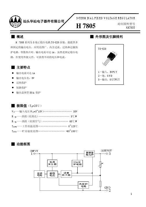
█ 外形图及引脚排列
TO-220
█ 主要特点
输出电流可达 1A 输出电压有:5V 过热保护 短路保护 输出晶体管 SOA 保护
7805三端稳压器,历代电子人青春和辉煌的见证者

7805三端稳压器,历代电子人青春和辉煌的见证者78xx系列三端集成稳压器诞生于上世纪70年代末80年代初,距今已有近40年的历史。
第一代78xx系列的使用者现在已近60岁,78xx见证了他们的青春和辉煌。
78xx系类电源芯片已经写进了大学模拟电路教材,并持续影响着大学生和电子工作者,对电源芯片的发展产生了深远的影响。
78xx系列主要的产品有7815,7812,7809和7805,分别表示输出电压为15V,12V,9V和5V。
因为八十年代初诞生的8051系列单片机是5V供电的,所以7805三端稳压器使用非常广泛。
现在电源芯片种类繁多,无论是转换效率还是封装都比7805优秀很多,但是7805依然很畅销。
7805三端稳压器应用较多的主要有三种型号,分别是7805,78M05,78L05,他们主要在输出电流上存在较大区别。
7805最大能提供1A的电流:能满足大多数5V产品对电源电流的要求。
78M05最大能提供500mA的电流:适用于中低功耗的需求;78L05最大能提供100mA的电流:适用于低功耗的需求;正确估算电路的功耗对芯片选型至关重要,笔者曾经做过一款正弦波驱动的BLDC控制板,为了尽可能的减小电路板尺寸,电源芯片选择了78L05,结果在调试的时候发现电源芯片发热严重,不得以重新选型了电源芯片。
三种类型的7805电源芯片78xx系列三端稳压器,转换效率低、发热严重,但是目前仍然被广泛应用,究其原因有如下个:1) 价格便宜,目前批量价格几毛钱,78L05价格更低;2)外围电路简单,只需要几个电容就可以稳定的工作;3)宽压输入,输入电压最大可达36V。
7805典型电路从图中可以看出,只需要两个电容,7805就可以稳定的输出5V,极大的简化了电路设计的复杂度。
7805电源模块7805电源芯片封装类型繁多,常用的封装类型有:TO-220,TO-252,SOT89。
7805芯片常用封装78xx三端稳压器是输出正电源的,与之相对的是79xx系列三端稳压器,输出的是负电压。
7805手册

LM78XX/LM78XXA 3-Terminal 1A Positive Voltage Regulator May 2006The LM78XX series of three terminal positive regulators are available in the TO-220 package and with severalfixed output voltages, making them useful in a wide range of applications. Each type employs internal current limiting, thermal shut down and safe operating area pro-tection, making it essentially indestructible. If adequate heat sinking is provided, they can deliver over 1A output current. Although designed primarily as fixed voltageLM78XX/LM78XXA 3-Terminal 1A Positive Voltage RegulatorLM78XX/LM78XXA 3-Terminal 1A Positive Voltage RegulatorElectrical Characteristics (LM7805)Refer to the test circuits. -40°C < T J < 125°C, I O = 500mA, V I = 10V , C I = 0.1 µ F , unless otherwise specified.Notes:1.Load and line regulation are specified at constant junction temperature. Changes in V O due to heating effects mustbe taken into account separately. Pulse testing with low duty is used.2.These parameters, although guaranteed, are not 100% tested in production.SymbolParameterConditionsMin.Typ.Max.UnitV OOutput VoltageT J = +25°C4.85.0 5.2V5mA ≤ I O ≤ 1A, P O ≤ 15W, V I = 7V to 20V4.755.0 5.25ReglineLine Regulation (1)T J = +25°C V O = 7V to 25V – 4.0100mV V I = 8V to 12V – 1.650.0Regload Load Regulation (1) T J = +25°C I O = 5mA to 1.5A –9.0100mV I O = 250mA to 750mA– 4.050.0I Q Quiescent CurrentT J = +25°C– 5.08.0mA ∆ I Q Quiescent Current Change I O = 5mA to 1A–0.030.5mA V I = 7V to 25V–0.3 1.3 ∆ V O / ∆ T Output Voltage Drift (2) I O = 5mA–-0.8–mV/°C V N Output Noise Voltage f = 10Hz to 100kHz, T A = +25°C –42.0– µ V/V O RR Ripple Rejection (2) f = 120Hz, V O = 8V to 18V 62.073.0–dB V DROP Dropout Voltage I O = 1A, T J = +25°C – 2.0–V r O Output Resistance (2) f = 1kHz–15.0–m Ω I SC Short Circuit Current V I = 35V , T A = +25°C –230–mA I PKPeak Current (2)T J= +25°C–2.2–ALM78XX/LM78XXA 3-Terminal 1A Positive Voltage RegulatorElectrical Characteristics (LM7806) (Continued)Refer to the test circuits. -40°C < T J < 125°C, I O = 500mA, V I = 11V , C I = 0.33 µ F , C O = 0.1 µ F , unless otherwise specified.Notes:3.Load and line regulation are specified at constant junction temperature. Changes in V O due to heating effects mustbe taken into account separately. Pulse testing with low duty is used.4.These parameters, although guaranteed, are not 100% tested in production.SymbolParameterConditionsMinTyp.Max.UnitV OOutput VoltageT J = +25°C5.756.0 6.25V5mA ≤ I O ≤ 1A, P O ≤ 15W, V I = 8.0V to 21V5.76.0 6.3Regline Line Regulation (3) T J = +25°C V I = 8V to 25V – 5.0120mV V I = 9V to 13V – 1.560.0Regload Load Regulation (3) T J = +25°C I O = 5mA to 1.5A –9.0120mV I O = 250mA to 750mA– 3.060.0I Q Quiescent Current T J = +25°C– 5.08.0mA ∆ I Q Quiescent Current ChangeI O = 5mA to 1A ––0.5mA V I = 8V to 25V –– 1.3 ∆ V O / ∆ T Output Voltage Drift (4) I O = 5mA–-0.8–mV/°C V N Output Noise Voltage f = 10Hz to 100kHz, T A = +25°C –45.0– µ V/V O RR Ripple Rejection (4) f = 120Hz, V O= 8V to 18V 62.073.0–dB V DROP Dropout Voltage I O = 1A, T J = +25°C – 2.0–V r O Output Resistance (4) f = 1kHz–19.0–m ΩI SC Short Circuit Current V I = 35V , T A = +25°C –250–mA I PKPeak Current (4)T J = +25°C–2.2–A5.Load and line regulation are specified at constant junction temperature. Changes in V O due to heating effects mustbe taken into account separately. Pulse testing with low duty is used.6.These parameters, although guaranteed, are not 100% tested in production.7.Load and line regulation are specified at constant junction temperature. Changes in V O due to heating effects mustbe taken into account separately. Pulse testing with low duty is used.8.These parameters, although guaranteed, are not 100% tested in production.I PK Peak Current(10)T J = +25°C– 2.2–ANotes:9.Load and line regulation are specified at constant junction temperature. Changes in V O due to heating effects mustbe taken into account separately. Pulse testing with low duty is used.10.These parameters, although guaranteed, are not 100% tested in production.11.Load and line regulation are specified at constant junction temperature. Changes in V O due to heating effects mustbe taken into account separately. Pulse testing with low duty is used.12.These parameters, although guaranteed, are not 100% tested in production.13.Load and line regulation are specified at constant junction temperature. Changes in V O due to heating effects mustbe taken into account separately. Pulse testing with low duty is used.14.These parameters, although guaranteed, are not 100% tested in production.15.Load and line regulation are specified at constant junction temperature. Changes in V O due to heating effects mustbe taken into account separately. Pulse testing with low duty is used.16.These parameters, although guaranteed, are not 100% tested in production.17.Load and line regulation are specified at constant junction temperature. Changes in V O due to heating effects mustbe taken into account separately. Pulse testing with low duty is used.18.These parameters, although guaranteed, are not 100% tested in production.r O Output Resistance(20) f = 1kHz–17.0–mΩI SC Short Circuit Current V I = 35V, T A = +25°C–250–mAI PK Peak Current(20)T J = +25°C– 2.2–ANotes:19.Load and line regulation are specified at constant junction temperature. Changes in V O due to heating effects mustbe taken into account separately. Pulse testing with low duty is used.20.These parameters, although guaranteed, are not 100% tested in production.r O Output Resistance(22) f = 1kHz–17.0–mΩI SC Short Circuit Current V I = 35V, T A = +25°C–250–mAI PK Peak Current(22)T J = +25°C– 2.2–ANotes:21.Load and line regulation are specified at constant junction temperature. Changes in V O due to heating effects mustbe taken into account separately. Pulse testing with low duty is used.22.These parameters, although guaranteed, are not 100% tested in production.V DROP Dropout Voltage I O = 1A, T J = +25°C– 2.0–V r O Output Resistance(24) f = 1kHz–18.0–mΩI SC Short Circuit Current V I = 35V, T A = +25°C–250–mAI PK Peak Current(24)T J = +25°C– 2.2–ANotes:23.Load and line regulation are specified at constant junction temperature. Changes in V O due to heating effects mustbe taken into account separately. Pulse testing with low duty is used.24.These parameters, although guaranteed, are not 100% tested in production.Notes:25.Load and line regulation are specified at constant junction temperature. Changes in V O due to heating effects mustbe taken into account separately. Pulse testing with low duty is used.26.These parameters, although guaranteed, are not 100% tested in production.RR Ripple Rejection (26) f = 120Hz, I O = 500mA, V I = 12V to 22V –62.0–dB V DROP Dropout Voltage I O = 1A, T J = +25°C – 2.0–V r O Output Resistance (26) f = 1kHz–17.0–m ΩI SC Short Circuit Current V I = 35V , T A = +25°C –250–mA I PKPeak Current (26)T J = +25°C–2.2–Ar O Output Resistance(28) f = 1kHz–17.0–mΩI SC Short Circuit Current V I = 35V, T A = +25°C–250–mAI PK Peak Current(28)T J = +25°C– 2.2–ANotes:27.Load and line regulation are specified at constant junction temperature. Changes in V O due to heating effects mustbe taken into account separately. Pulse testing with low duty is used.28.These parameters, although guaranteed, are not 100% tested in production.V DROP Dropout Voltage I O = 1A, T J = +25°C– 2.0–V r O Output Resistance(30) f = 1kHz–18.0–mΩI SC Short Circuit Current V I = 35V, T A = +25°C–250–mAI PK Peak Current(30)T J = +25°C– 2.2–ANote:29.Load and line regulation are specified at constant junction temperature. Changes in V O due to heating effects mustbe taken into account separately. Pulse testing with low duty is used.30.These parameters, although guaranteed, are not 100% tested in production.V DROP Dropout Voltage I O = 1A, T J = +25°C– 2.0–V r O Output Resistance(32) f = 1kHz–19.0–mΩI SC Short Circuit Current V I = 35V, T A = +25°C–250–mAI PK Peak Current(32)T J = +25°C– 2.2–ANotes:31.Load and line regulation are specified at constant junction temperature. Changes in V O due to heating effects mustbe taken into account separately. Pulse testing with low duty is used.32.These parameters, although guaranteed, are not 100% tested in production.V DROP Dropout Voltage I O = 1A, T J = +25°C– 2.0–V r O Output Resistance(34) f = 1kHz–19.0–mΩI SC Short Circuit Current V I = 35V, T A = +25°C–250–mAI PK Peak Current(34)T J = +25°C– 2.2–ANotes:33.Load and line regulation are specified at constant junction temperature. Changes in V O due to heating effects mustbe taken into account separately. Pulse testing with low duty is used.34.These parameters, although guaranteed, are not 100% tested in production.V DROP Dropout Voltage I O = 1A, T J = +25°C– 2.0–V r O Output Resistance(36) f = 1kHz–20.0–mΩI SC Short Circuit Current V I = 35V, T A = +25°C–250–mAI PK Peak Current(36)T J = +25°C– 2.2–ANotes:35.Load and line regulation are specified at constant junction temperature. Changes in V O due to heating effects mustbe taken into account separately. Pulse testing with low duty is used.36.These parameters, although guaranteed, are not 100% tested in production.LM78XX/LM78XXA 3-Terminal 1A Positive Voltage RegulatorLM78XX/LM78XXA 3-Terminal 1A Positive Voltage Regulator。
7805常用电路
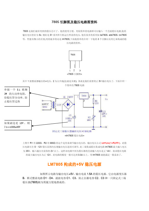
7805引脚图及稳压电路图资料7805是我们最常用到的稳压芯片了,他的使用方便,用很简单的电路即可以输入一个直流稳压电源,他的输出电压恰好为5v ,刚好是51系列单片机运行所需的电压,他有很多的系列如ka7805,ads7805,cw7805等,性能有微小的差别,用的最多的还是lm7805,下面我简单的介绍一下他的3个引脚以及用它来构成的稳压电路的资料。
<7805引脚图>其中1接整流器输出的+电压,2为公共地(也就是负极),3就是我们需要的正5V 输出电压了,下面介绍一个简单的7805电路<lm7805稳压电路>上图中R1用220Ω,R2用680Ω的这个是用来调节输出电压的。
输出电压公式Uo ≈Uxx(1+R2/R1),此稳压电路可在5~12V 稳压范围内实现输出电压连续可调节。
此三端集成稳压集成电路lm7805最大输入电压为35V ,输入输出差需保持2V 以上,这样该电路中因为稳压器的直流输入电压是正14V ,故该稳压电路的最大输出电压为正12V 。
此电路的精度一般可达到0.04以上,用lm7805就能满足一般需求了。
LM7805构成的+5V 稳压电源如图所示电路为输出电压+5V 、输出电流1.5A 的稳压电源。
它由电源变压器B ,桥式整流电路D1~D4,滤波电容C1、C3,防止自激电容C2、C3和一只固定式三端稳压器(7805)极为简捷方便地搭成的。
220V交流市电通过电源变压器变换成交流低压,再经过桥式整流电路D1~D4和滤波电容C1的整流和滤波,在固定式三端稳压器LM7805的Vin和GND两端形成一个并不十分稳定的直流电压(该电压常常会因为市电电压的波动或负载的变化等原因而发生变化)。
此直流电压经过LM7805的稳压和C3的滤波便在稳压电源的输出端产生了精度高、稳定度好的直流输出电压。
本稳压电源可作为TTL电路或单片机电路的电源。
三端稳压器是一种标准化、系列化的通用线性稳压电源集成电路,以其体积小、成本低、性能好、工作可靠性高、使用简捷方便等特点,成为目前稳压电源中应用最为广泛的一种单片式集成稳压器件。
7805稳压芯片,7805芯片介绍

7805 稳压芯片,7805 芯片介绍
7805 是我们最常用到的稳压芯片了,他的使用方便,用很简单的电
路即可以输入一个直流稳压电源,他的输出电压恰好为5v,刚好是51 系列
单片机运行所需的电压,他有很多的系列如ka7805,ads7805,cw7805 等,
性能有微小的差别,用的最多的还是lm7805。
7805 结构组成是用78/79 系列三端稳压IC 来组成稳压电源所需的外
围元件极少,7805 三端稳压集成电路电路内部还有过流、过热及调整管的保护电路,使用起来可靠、方便,而且价格便宜。
该系列集成稳压IC 型号中的78 或79 后面的数字代表该三端集成稳压电路的输出电压,如7806 表示输出
电压为正6V,7909 表示输出电压为负9V。
因为三端固定集成稳压电路的使用方便,电子制作中经常采用。
在实际应用中,应在三端集成稳压电路上安装足够大的散热器(当然小功率的条件下不用)。
当稳压管温度过高时,稳压性能将变差,甚至损坏。
当制作中需要一个能输出1.5A 以上电流的稳压电源,通常采用几块三端稳压电路并联起来,使其最大输出电流为N 个1.5A,但应用时需注意:并联使用的集成稳压电路应采用同一厂家、同一批号的产品,以保证参数的一致。
7805稳压器
7805管脚78**系列的稳压集成块的极限输入电压是36V,最低输入电压为输出电压的3-4V以上。
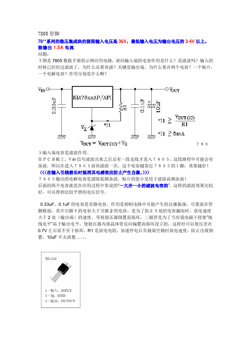
能输出1.5A电流问题:下图是7805数据手册的示例应用电路,请问输入端的电容作用是什么?是滤波吗?输入的时候已经经过滤波了,为什么还要再滤?关键是输出端,为什么要并两个电容?一个贴片,一个电解电容?作用分别是什么啊?7805输入端电容是滤波作用。
在PCB板上,Vin信号滤波出来之后总有一段走线才进入7805,这段路程中可能会有杂波,所以在进入7805前再滤波一次,这个电容越靠近7805的1脚,效果越好!(((在输入引线教长时抵消其电感效应防止产生自激,)))7805输出的电解电容是滤除低频杂波,贴片的值小是用于滤除高频杂波!后面的两个电容就是在应用过程中常说的“一大并一小的滤波电容的”。
这样的滤波效果比较好,可以得到比较平滑的电压信号。
0.33uF,0.1uF的电容是旁路电容,作用是抑制电路中可能产生的自激振荡,尽量放在管脚根部,其中引脚1的电容大于引脚2的电容,是为了防止1处的电容漏电时,放电速度大于2处(输出端)的速度,导致稳压器倒置而损坏,二极管是为了当有强电磁干扰使“地线电平”高于输出电平,使稳压器内部晶体管反向偏置而损坏设立的,这样经可以使压差在0.7V左右而不至于损坏,R1是放电电阻,加速停电后负载端空载时放电速度,防止出现倒置,10uF不太清楚。
7805典型应用电路图:78XX系列集成稳压器的典型应用电路如下图所示,这是一个输出正5V直流电压的稳压电源电路。
IC采用集成稳压器7805,C1、C2分别为输入端和输出端滤波电容,RL为负载电阻。
当输出电较大时,7805应配上散热板。
下图为提高输出电压的应用电路。
稳压二极管VD1串接在78XX稳压器2脚与地之间,可使输出电压Uo得到一定的提高,输出电压Uo为78XX稳压器输出电压与稳压二极管VC1稳压值之和。
VD2是输出保护二极管,一旦输出电压低于VD1稳压值时,VD2导通,将输出电流旁路,保护7800稳压器输出级不被损坏。
7805A_datasheet

DescriptionThe 7805A can provide local on-card regulation, eliminating thedistribution problems associated with single point regulation. Each employs internal current limiting, thermal shut-down and safe operating area protection, deliver over 1A output current. Although designed primarily as fixed voltage regulators, these devices can be used with external components to obtain adjustable voltages and currents.Features• Output Current In Excess of 1A • Output Voltage of 5V• Internal Short-Circuit Current Limiting & Thermal Overload Protection • Guaranteed In Extended Temperature RangeAbsolute Maximum Ratings (T A =25°C)Characteristic Symbol Rating Unit Input Voltage V IN 40 VPower Dissipation P D Internally limited (Note)Operating Temperature T opr -30 to 85 o C Storage Temperature T stg-55 to 150oCJunction TemperatureT j 150 o CNote: (1)T A =25oC, , TO-252: 1W, TO-220AB: 2.7W(2)T C =25oC, All package: 10WThermal DataCharacteristicSymbolTO-252TO-220ABUnitThermal Resistance Junction-Case R th(j-c) 12.5 12.5 o C/W Thermal Resistance Junction-AmbientR th(j-a) 12547oC/WSchematic Diagram & Equivalent Circuit7805A3- Terminal Positive Voltage Regulators7805A Series Electrical CharacteristicsV IN =10V, I OUT =500mA, C IN =0.33uF, C OUT =0.1uF, 0°C ≤T J ≤125°C (unless otherwise specified) 7805AJ/AE SymbolParameterConditionsMinTypMaxUnitsT J =25°C, I OUT =500mA4.85 55.155mA ≤I OUT ≤1AV O Output Voltage7V ≤V IN ≤25V, P OUT ≤15W4.85 55.15VT J =25°C, 7V ≤V IN ≤25V - 3 50ΔV O Line Regulation T J =25°C, 8V ≤V IN ≤12V - 1 25 mVT J =25°C, 5mA ≤I OUT ≤1A - 15 100ΔV OLoad RegulationT J =25°C, 250mA ≤I OUT ≤750mA - 5 50 mVI B Quiescent Current I OUT =5mA, T J =25°C- 3.9 8 mA I OUT =500mA, 7V ≤V IN ≤25V, T J =25oC - - 1.3ΔI B Quiescent Current Change5mA ≤I OUT ≤1A, V IN =10V, T J =25oC - - 0.5 mAeNOutput Noise VoltageB=10Hz~100KHz, I OUT =50mA, T J =25°C - 50 - uV/V O RR Ripple Rejection 10V ≤V IN ≤18V, f=120Hz, I OUT =50mA, T J =25oC 57 73 - dB VD Dropout Voltage T J =25°C, I OUT =1A - 2 2.5 V R O Output Resistance f =1KHz- 17 - m Ω I SC Short Circuit Current T J =25°C - 2.3 2.8 A ΔV O /ΔTOutput Voltage Drift0oC ≤T J ≤125oC- - 0.6 mV/°CTest CircuitsApplication CircuitsCharacteristics CurveTO-252 DimensionTO-220AB DimensionOrdering InformationPart Number V OUT : Package 7805AJ 5V ±0.15V TO-252 7805AE 5V ±0.15V TO-220ABNote: Green label is used for pb-free packing Pin Style: 1.Input 2.Ground 3.Output Material:• Lead solder plating: Sn60/Pb40 (Normal), Sn/3.0Ag/0.5Cu or Pure-Tin (Pb-free) • Mold Compound: Epoxy resin family,flammability solid burning class: UL94V-0Soldering Methods for Orister’s Products1. Storage environment: Temperature=10o C~35o C Humidity=65%±15%2. Reflow soldering of surface-mount devicesProfile FeatureSn-Pb Eutectic AssemblyPb-Free AssemblyAverage ramp-up rate (T L to T P ) <3o C/sec <3o C/sec Preheat- Temperature Min (Ts min ) - Temperature Max (Ts max ) - Time (min to max) (ts) 100o C 150o C 60~120 sec150o C 200o C 60~180 secTsmax to T L - Ramp-up Rate <3o C/sec<3o C/secTime maintained above: - Temperature (T L ) - Time (t L )183o C 60~150 sec217o C 60~150 secPeak Temperature (T P ) 240o C +0/-5o C 260o C +0/-5o CTime within 5o C of actual Peak Temperature (t P ) 10~30 sec20~40 secRamp-down Rate<6o C/sec <6o C/sec Time 25o C to Peak Temperature <6 minutes<8 minutes3. Flow (wave) soldering (solder dipping)ProductsPeak temperatureDipping timePb devices. 245o C ±5o C 5sec ±1sec Pb-Free devices.260o C +0/-5o C5sec ±1sec。
超详细的7805简介与使用说明
- 1、下载文档前请自行甄别文档内容的完整性,平台不提供额外的编辑、内容补充、找答案等附加服务。
- 2、"仅部分预览"的文档,不可在线预览部分如存在完整性等问题,可反馈申请退款(可完整预览的文档不适用该条件!)。
- 3、如文档侵犯您的权益,请联系客服反馈,我们会尽快为您处理(人工客服工作时间:9:00-18:30)。
Rev. 1.0.0Features•Output Current up to 1A •Output V oltages of 5, 6, 8, 9, 10, 12, 15, 18, 24V•Thermal Overload Protection •Short Circuit Protection•Output Transistor Safe Operating Area ProtectionDescriptionThe KA78XX/KA78XXA series of three-terminal positive regulator are available in the TO-220/D-PAK package and with several fixed output voltages, making them useful in a wide range of applications. Each type employs internalcurrent limiting, thermal shut down and safe operating area protection, making it essentially indestructible. If adequate heat sinking is provided, they can deliver over 1A output current. Although designed primarily as fixed voltage regulators, these devices can be used with external components to obtain adjustable voltages and currents.TO-220D-PAK1. Input2. GND3. Output11Internal Block DigramKA78XX/KA78XXA3-Terminal 1A Positive Voltage RegulatorKA78XX/KA78XXAAbsolute Maximum RatingsElectrical Characteristics (KA7805/KA7805R)(Refer to test circuit ,0°C < T J < 125°C, I O = 500mA, V I =10V, C I = 0.33µF, C O =0.1µF, unless otherwise specified)Note:1. Load and line regulation are specified at constant junction temperature. Changes in V o due to heating effects must be takeninto account separately. Pulse testing with low duty is used.ParameterSymbol Value Unit Input Voltage (for V O = 5V to 18V)(for V O = 24V)V I V I 3540V V Thermal Resistance Junction-Cases (TO-220)R θJC 5°C/WThermal Resistance Junction-Air (TO-220)R θJA 65°C/WOperating Temperature Range (KA78XX/A/R)T OPR 0 ~ +125°C Storage Temperature RangeT STG-65 ~ +150°CParameterSymbolConditionsKA7805UnitMin.Typ.Max.Output VoltageV OT J =+25 o C4.85.0 5.25.0mA ≤Io ≤1.0A, P O ≤15W V I = 7V to 20V 4.75 5.0 5.25 V Line Regulation (Note1)Regline T J =+25 o C V O = 7V to 25V - 4.0100mV V I = 8V to 12V - 1.650Load Regulation (Note1)Regload T J =+25 o C I O = 5.0mA to1.5A -9100mV I O =250mA to 750mA -450Quiescent Current I Q T J =+25 o C - 5.08.0mA Quiescent Current Change ∆I Q I O = 5mA to 1.0A -0.030.5mA V I = 7V to 25V -0.3 1.3Output Voltage Drift ∆V O /∆T I O = 5mA--0.8-mV/ o C Output Noise Voltage V N f = 10Hz to 100KHz, T A =+25 o C -42-µV/V O Ripple Rejection RR f = 120HzV O = 8V to 18V 6273-dB Dropout Voltage V Drop I O = 1A, T J =+25 o C -2-V Output Resistance r O f = 1KHz-15-m ΩShort Circuit Current I SC V I = 35V, T A =+25 o C -230-mA Peak CurrentI PKT J =+25 o C- 2.2-AKA78XX/KA78XXAElectrical Characteristics (KA7806/KA7806R)(Refer to test circuit ,0°C < T J < 125°C, I O = 500mA, V I =11V, C I = 0.33µF, C O =0.1µF, unless otherwise specified)Note:1. Load and line regulation are specified at constant junction temperature. Changes in V O due to heating effects must be takeninto account separately. Pulse testing with low duty is used.ParameterSymbolConditionsKA7806UnitMin.Typ.Max.Output VoltageV OT J =+25 o C5.756.0 6.255.0mA ≤I O ≤1.0A, P O ≤15W V I = 8.0V to 21V 5.7 6.0 6.3 V Line Regulation (Note1)Regline T J =+25 o C V I = 8V to 25V -5120mV V I = 9V to 13V - 1.560Load Regulation (Note1)Regload T J =+25 o C I O =5mA to 1.5A -9120mV I O =250mA to750mA -360Quiescent Current I Q T J =+25 o C - 5.08.0mA Quiescent Current Change ∆I Q I O = 5mA to 1A --0.5mA V I = 8V to 25V -- 1.3Output Voltage Drift ∆V O /∆T I O = 5mA--0.8-mV/ o C Output Noise Voltage V N f = 10Hz to 100KHz, T A =+25 o C -45-µV/Vo Ripple Rejection RR f = 120HzV I = 9V to 19V 5975-dB Dropout Voltage V Drop I O = 1A, T J =+25 o C -2-V Output Resistance r O f = 1KHz-19-m ΩShort Circuit Current I SC V I = 35V, T A =+25 o C -250-mA Peak CurrentI PKT J =+25 o C- 2.2-AKA78XX/KA78XXAElectrical Characteristics (KA7808/KA7808R)(Refer to test circuit ,0°C < T J < 125°C, I O = 500mA, V I =14V, C I = 0.33µF, C O =0.1µF, unless otherwise specified)Note:1. Load and line regulation are specified at constant junction temperature. Changes in V O due to heating effects must be takeninto account separately. Pulse testing with low duty is used.ParameterSymbolConditionsKA7808UnitMin.Typ.Max.Output VoltageV OT J =+25 o C7.78.08.35.0mA ≤ I O ≤1.0A, P O ≤15W V I = 10.5V to 23V 7.68.08.4 V Line Regulation (Note1)ReglineT J =+25 o C V I = 10.5V to 25V - 5.0160mV V I = 11.5V to 17V - 2.080Load Regulation (Note1)Regload T J =+25 o C I O = 5.0mA to 1.5A-10160mV I O = 250mA to 750mA - 5.080Quiescent Current I Q T J =+25 o C - 5.08.0mA Quiescent Current Change ∆I Q I O = 5mA to 1.0A -0.050.5mA V I = 10.5A to 25V -0.5 1.0Output Voltage Drift ∆V O /∆T I O = 5mA--0.8-mV/ o C Output Noise Voltage V N f = 10Hz to 100KHz, T A =+25 o C -52-µV/Vo Ripple Rejection RR f = 120Hz, V I = 11.5V to 21.5V 5673-dB Dropout Voltage V Drop I O = 1A, T J =+25 o C -2-V Output Resistance r O f = 1KHz-17-m ΩShort Circuit Current I SC V I = 35V, T A =+25 o C -230-mA Peak CurrentI PKT J =+25 o C- 2.2-AKA78XX/KA78XXAElectrical Characteristics (KA7809/KA7809R)(Refer to test circuit ,0°C < T J < 125°C, I O = 500mA, V I =15V, C I = 0.33µF, C O =0.1µF, unless otherwise specified)Note:1. Load and line regulation are specified at constant junction temperature. Changes in V O due to heating effects must be takeninto account separately. Pulse testing with low duty is used.ParameterSymbolConditionsKA7809UnitMin.Typ.Max.Output VoltageV OT J =+25 o C8.6599.355.0mA ≤ I O ≤1.0A, P O ≤15W V I = 11.5V to 24V 8.699.4 V Line Regulation (Note1)Regline T J =+25 o C V I = 11.5V to 25V -6180mV V I = 12V to 17V -290Load Regulation (Note1)Regload T J =+25 o C I O = 5mA to 1.5A -12180mV I O = 250mA to 750mA -490Quiescent Current I Q T J =+25 o C - 5.08.0mA Quiescent Current Change ∆I Q I O = 5mA to 1.0A --0.5mA V I = 11.5V to 26V -- 1.3Output Voltage Drift ∆V O /∆T I O = 5mA--1-mV/ o C Output Noise Voltage V N f = 10Hz to 100KHz, T A =+25 o C -58-µV/Vo Ripple Rejection RR f = 120HzV I = 13V to 23V 5671-dB Dropout Voltage V Drop I O = 1A, T J =+25 o C -2-V Output Resistance r O f = 1KHz-17-m ΩShort Circuit Current I SC V I = 35V, T A =+25 o C -250-mA Peak CurrentI PKT J = +25 o C- 2.2-AElectrical Characteristics (KA7810)(Refer to test circuit ,0°C < T J < 125°C, I O = 500mA, V I =16V, C I = 0.33µF, C O =0.1µF, unless otherwise specified)Note:1. Load and line regulation are specified at constant junction temperature. Changes in V O due to heating effects must be takeninto account separately. Pulse testing with low duty is used.ParameterSymbolConditionsKA7810UnitMin.Typ.Max.Output VoltageV OT J =+25 o C9.61010.45.0mA ≤ I O ≤ 1.0A, P O ≤ 15W V I = 12.5V to 25V 9.51010.5 V Line Regulation (Note1)Regline T J =+25 o C V I = 12.5V to 25V -10200mV V I = 13V to 25V -3100Load Regulation (Note1)Regload T J =+25 o C I O = 5mA to 1.5A -12200mV I O = 250mA to 750mA -4400Quiescent Current I Q T J =+25 o C - 5.18.0mA Quiescent Current Change ∆I Q I O = 5mA to 1.0A --0.5mA V I = 12.5V to 29V -- 1.0Output Voltage Drift ∆V O /∆T I O = 5mA--1-mV/ o C Output Noise Voltage V N f = 10Hz to 100KHz, T A =+25 o C -58-µV/Vo Ripple Rejection RR f = 120HzV I = 13V to 23V 5671-dB Dropout Voltage V Drop I O = 1A, T J =+25 o C -2-V Output Resistance r O f = 1KHz-17-m ΩShort Circuit Current I SC V I = 35V, T A =+25 o C -250-mA Peak CurrentI PKT J =+25 o C- 2.2-AElectrical Characteristics (KA7812/KA7812R)(Refer to test circuit ,0°C < T J < 125°C, I O = 500mA, V I =19V, C I = 0.33µF, C O =0.1µF, unless otherwise specified)Note:1. Load and line regulation are specified at constant junction temperature. Changes in V O due to heating effects must be takeninto account separately. Pulse testing with low duty is used.ParameterSymbolConditionsKA7812/KA7812R UnitMin.Typ.Max.Output VoltageV OT J =+25 o C11.51212.55.0mA ≤ I O ≤1.0A, P O ≤15W V I = 14.5V to 27V 11.41212.6 V Line Regulation (Note1)ReglineT J =+25 o CV I = 14.5V to 30V -10240mV V I = 16V to 22V - 3.0120Load Regulation (Note1)Regload T J =+25 o C I O = 5mA to 1.5A -11240mV I O = 250mA to 750mA - 5.0120Quiescent Current I Q T J =+25 o C - 5.18.0mA Quiescent Current Change ∆I Q I O = 5mA to 1.0A -0.10.5mA V I = 14.5V to 30V -0.5 1.0Output Voltage Drift ∆V O /∆T I O = 5mA--1-mV/ o C Output Noise Voltage V N f = 10Hz to 100KHz, T A =+25 o C -76-µV/Vo Ripple Rejection RR f = 120HzV I = 15V to 25V 5571-dB Dropout Voltage V Drop I O = 1A, T J =+25 o C -2-V Output Resistance r O f = 1KHz-18-m ΩShort Circuit Current I SC V I = 35V, T A =+25 o C -230-mA Peak CurrentI PKT J = +25 o C- 2.2-AKA78XX/KA78XXAElectrical Characteristics (KA7815)(Refer to test circuit ,0°C < T J < 125°C, I O = 500mA, V I =23V, C I = 0.33µF, C O =0.1µF, unless otherwise specified)Note:1. Load and line regulation are specified at constant junction temperature. Changes in V O due to heating effects must be takeninto account separately. Pulse testing with low duty is used.ParameterSymbolConditionsKA7815UnitMin.Typ.Max.Output VoltageV OT J =+25 o C14.41515.65.0mA ≤ I O ≤1.0A, P O ≤15W V I = 17.5V to 30V 14.251515.75 V Line Regulation (Note1)Regline T J =+25 o C V I = 17.5V to 30V -11300mV V I = 20V to 26V -3150Load Regulation (Note1)Regload T J =+25 o C I O = 5mA to 1.5A -12300mV I O = 250mA to 750mA -4150Quiescent Current I Q T J =+25 o C - 5.28.0mA Quiescent Current Change ∆I Q I O = 5mA to 1.0A --0.5mA V I = 17.5V to 30V -- 1.0Output Voltage Drift ∆V O /∆T I O = 5mA--1-mV/ o C Output Noise Voltage V N f = 10Hz to 100KHz, T A =+25 o C -90-µV/Vo Ripple Rejection RR f = 120HzV I = 18.5V to 28.5V 5470-dB Dropout Voltage V Drop I O = 1A, T J =+25 o C -2-V Output Resistance r O f = 1KHz-19-m ΩShort Circuit Current I SC V I = 35V, T A =+25 o C -250-mA Peak CurrentI PKT J =+25 o C- 2.2-AKA78XX/KA78XXAElectrical Characteristics (KA7818)(Refer to test circuit ,0°C < T J < 125°C, I O = 500mA, V I =27V, C I = 0.33µF, C O =0.1µF, unless otherwise specified)Note:1. Load and line regulation are specified at constant junction temperature. Changes in V O due to heating effects must be takeninto account separately. Pulse testing with low duty is used.ParameterSymbolConditionsKA7818UnitMin.Typ.Max.Output VoltageV OT J =+25 o C17.31818.75.0mA ≤ I O ≤1.0A, P O ≤15W V I = 21V to 33V 17.11818.9 V Line Regulation (Note1)Regline T J =+25 o C V I = 21V to 33V -15360mV V I = 24V to 30V -5180Load Regulation (Note1)Regload T J =+25 o C I O = 5mA to 1.5A -15360mV I O = 250mA to 750mA - 5.0180Quiescent Current I Q T J =+25 o C - 5.28.0mA Quiescent Current Change ∆I Q I O = 5mA to 1.0A --0.5mA V I = 21V to 33V --1Output Voltage Drift ∆V O /∆T I O = 5mA--1-mV/ o C Output Noise Voltage V N f = 10Hz to 100KHz, T A =+25 o C -110-µV/Vo Ripple Rejection RR f = 120HzV I = 22V to 32V 5369-dB Dropout Voltage V Drop I O = 1A, T J =+25 o C -2-V Output Resistance r O f = 1KHz-22-m ΩShort Circuit Current I SC V I = 35V, T A =+25 o C -250-mA Peak CurrentI PKT J =+25 o C-2.2-AKA78XX/KA78XXAElectrical Characteristics (KA7824)(Refer to test circuit ,0°C < T J < 125°C, I O = 500mA, V I =33V, C I = 0.33µF, C O =0.1µF, unless otherwise specified)Note:1. Load and line regulation are specified at constant junction temperature. Changes in V O due to heating effects must be takeninto account separately. Pulse testing with low duty is used.ParameterSymbolConditionsKA7824UnitMin.Typ.Max.Output VoltageV OT J =+25 o C2324255.0mA ≤ I O ≤ 1.0A, P O ≤ 15W V I = 27V to 38V 22.82425.25 V Line Regulation (Note1)ReglineT J =+25 o CV I = 27V to 38V -17480mV V I = 30V to 36V -6240Load Regulation (Note1)Regload T J =+25 o C I O = 5mA to 1.5A -15480mV I O = 250mA to 750mA - 5.0240Quiescent Current I Q T J =+25 o C - 5.28.0mA Quiescent Current Change ∆I QI O = 5mA to 1.0A -0.10.5mA V I = 27V to 38V-0.51Output Voltage Drift ∆V O /∆T I O = 5mA --1.5-mV/ o C Output Noise Voltage V N f = 10Hz to 100KHz, T A =+25 o C -60-µV/Vo Ripple Rejection RR f = 120HzV I = 28V to 38V 5067-dB Dropout Voltage V Drop I O = 1A, T J =+25 o C -2-V Output Resistance r O f = 1KHz-28-m ΩShort Circuit Current I SC V I = 35V, T A =+25 o C -230-mA Peak CurrentI PKT J =+25 o C- 2.2-AKA78XX/KA78XXAElectrical Characteristics (KA7805A)(Refer to the test circuits. 0o C < T J < +125 o C, I o =1A, V I = 10V, C I =0.33µF, C O =0.1µF, unless otherwise speci-fied)Note:1. Load and line regulation are specified at constant junction temperature. Change in V O due to heating effects must be takeninto account separately. Pulse testing with low duty is used.ParameterSymbol ConditionsMin.Typ.Max.UnitOutput VoltageV OT J =+25 o C4.955.1V I O = 5mA to 1A, P O ≤ 15W V I = 7.5V to 20V 4.85 5.2Line Regulation (Note1)ReglineV I = 7.5V to 25V I O = 500mA-550mV V I = 8V to 12V -350T J =+25 o CV I = 7.3V to 20V -550V I = 8V to 12V- 1.525Load Regulation (Note1)RegloadT J =+25 o CI O = 5mA to 1.5A -9100mV I O = 5mA to 1A -9100I O = 250mA to 750mA -450Quiescent Current I Q T J =+25 o C - 5.0 6.0mA Quiescent Current Change∆I Q I O = 5mA to 1A--0.5mA V I = 8 V to 25V, I O = 500mA --0.8V I = 7.5V to 20V, T J =+25 o C --0.8Output Voltage Drift ∆V/∆T Io = 5mA--0.8-mV/ o C Output Noise Voltage V N f = 10Hz to 100KHz T A =+25 o C-10-µV/Vo Ripple Rejection RR f = 120Hz, I O = 500mA V I = 8V to 18V -68-dB Dropout Voltage V Drop I O = 1A, T J =+25 o C -2-V Output Resistance r O f = 1KHz-17-m ΩShort Circuit Current I SC V I = 35V, T A =+25 o C -250-mA Peak CurrentI PKT J = +25 o C- 2.2-AKA78XX/KA78XXAElectrical Characteristics (KA7806A)(Refer to the test circuits. 0o C < T J < +125 o C, I o =1A, V I = 11V, C I =0.33µF, C O =0.1µF, unless otherwise speci-fied)Note:1. Load and line regulation are specified at constant junction temperature. Change in V O due to heating effects must be takeninto account separately. Pulse testing with low duty is used.ParameterSymbol ConditionsMin.Typ.Max.UnitOutput VoltageV OT J =+25 o C5.5866.12V I O = 5mA to 1A, P O ≤ 15W V I = 8.6V to 21V 5.766 6.24Line Regulation (Note1)ReglineV I = 8.6V to 25V I O = 500mA-560mV V I = 9V to 13V -360T J =+25 o CV I = 8.3V to 21V -560V I = 9V to 13V- 1.530Load Regulation (Note1)RegloadT J =+25 o CI O = 5mA to 1.5A -9100mV I O = 5mA to 1A -4100I O = 250mA to 750mA - 5.050Quiescent Current I Q T J =+25 o C - 4.3 6.0mA Quiescent Current Change ∆I Q I O = 5mA to 1A--0.5mA V I = 9V to 25V, I O = 500mA --0.8V I = 8.5V to 21V, T J =+25 o C --0.8Output Voltage Drift ∆V/∆T I O = 5mA--0.8-mV/ o C Output Noise Voltage V N f = 10Hz to 100KHz T A =+25 o C-10-µV/Vo Ripple Rejection RR f = 120Hz, I O = 500mA V I = 9V to 19V -65-dB Dropout Voltage V Drop I O = 1A, T J =+25 o C -2-V Output Resistance r O f = 1KHz-17-m ΩShort Circuit Current I SC V I = 35V, T A =+25 o C -250-mA Peak CurrentI PKT J =+25 o C- 2.2-AKA78XX/KA78XXAElectrical Characteristics (KA7808A)(Refer to the test circuits. 0o C < T J < +125 o C, I o =1A, V I = 14V, C I =0.33µF, C O =0.1µF, unless otherwise speci-fied)Note:1. Load and line regulation are specified at constant junction temperature. Change in V O due to heating effects must be takeninto account separately. Pulse testing with low duty is used.ParameterSymbol ConditionsMin.Typ.Max.UnitOutput VoltageV OT J =+25 o C7.8488.16V I O = 5mA to 1A, P O ≤15W V I = 10.6V to 23V 7.788.3Line Regulation (Note1)ReglineV I = 10.6V to 25V I O = 500mA-680mV V I = 11V to 17V -380T J =+25 o CV I = 10.4V to 23V -680V I = 11V to 17V-240Load Regulation (Note1)RegloadT J =+25 o CI O = 5mA to 1.5A -12100mV I O = 5mA to 1A -12100I O = 250mA to 750mA -550Quiescent Current I Q T J =+25 o C - 5.0 6.0mA Quiescent Current Change ∆I Q I O = 5mA to 1A--0.5mA V I = 11V to 25V, I O = 500mA --0.8V I = 10.6V to 23V, T J =+25 o C --0.8Output Voltage Drift ∆V/∆T I O = 5mA--0.8-mV/ o C Output Noise Voltage V N f = 10Hz to 100KHz T A =+25 o C-10-µV/Vo Ripple Rejection RR f = 120Hz, I O = 500mA V I = 11.5V to 21.5V -62-dB Dropout Voltage V Drop I O = 1A, T J =+25 o C -2-V Output Resistance r O f = 1KHz-18-m ΩShort Circuit Current I SC V I = 35V, T A =+25 o C -250-mA Peak CurrentI PKT J =+25 o C- 2.2-AKA78XX/KA78XXAElectrical Characteristics (KA7809A)(Refer to the test circuits. 0o C < T J < +125 o C, I o =1A, V I = 15V, C I =0.33µF, C O =0.1µF, unless otherwise speci-fied)Note:1. Load and line regulation are specified at constant junction temperature. Change in V O due to heating effects must be takeninto account separately. Pulse testing with low duty is used.ParameterSymbolConditionsMin.Typ.Max.UnitOutput VoltageV OT J =+25°C8.829.09.18V I O = 5mA to 1A, P O ≤15W V I = 11.2V to 24V 8.659.09.35Line Regulation (Note1)ReglineV I = 11.7V to 25V I O = 500mA-690mV V I = 12.5V to 19V -445T J =+25°CV I = 11.5V to 24V -690 V I = 12.5V to 19V -245Load Regulation (Note1)RegloadT J =+25°CI O = 5mA to 1.0A -12100mV I O = 5mA to 1.0A -12100I O = 250mA to 750mA -550Quiescent Current I Q T J =+25 °C- 5.0 6.0mA Quiescent Current Change ∆I Q V I = 11.7V to 25V, T J =+25 °C --0.8mA V I = 12V to 25V, I O = 500mA --0.8I O = 5mA to 1.0A --0.5Output Voltage Drift ∆V/∆T I O = 5mA--1.0-mV/ °C Output Noise Voltage V N f = 10Hz to 100KHz T A =+25 °C-10-µV/Vo Ripple Rejection RR f = 120Hz, I O = 500mA V I = 12V to 22V -62-dB Dropout Voltage V Drop I O = 1A, T J =+25 °C - 2.0-V Output Resistance r O f = 1KHz-17-m ΩShort Circuit Current I SC V I = 35V, T A =+25 °C -250-mA Peak CurrentI PKT J =+25°C- 2.2-A(Refer to the test circuits. 0o C < T J < +125 o C, I o =1A, V I = 16V, C I =0.33µF, C O =0.1µF, unless otherwise speci-fied)Note:1. Load and line regulation are specified at constant junction temperature. Change in V O due to heating effects must be takeninto account separately. Pulse testing with low duty is used.ParameterSymbolConditionsMin.Typ.Max.UnitOutput VoltageV OT J =+25°C9.81010.2V I O = 5mA to 1A, P O ≤ 15W V I =12.8V to 25V 9.61010.4Line Regulation (Note1)ReglineV I = 12.8V to 26V I O = 500mA-8100mV V I = 13V to 20V -450 T J =+25 °CV I = 12.5V to 25V -8100 V I = 13V to 20V -350Load Regulation (Note1)RegloadT J =+25 °CI O = 5mA to 1.5A -12100mV I O = 5mA to 1.0A -12100 I O = 250mA to 750mA -550Quiescent Current I Q T J =+25 °C- 5.0 6.0mA Quiescent Current Change ∆I QV I = 13V to 26V, T J =+25 °C --0.5mA V I = 12.8V to 25V, I O = 500mA --0.8 I O = 5mA to 1.0A--0.5Output Voltage Drift ∆V/∆T I O = 5mA --1.0-mV/ °C Output Noise Voltage V N f = 10Hz to 100KHz T A =+25 °C-10-µV/Vo Ripple Rejection RR f = 120Hz, I O = 500mA V I = 14V to 24V -62-dB Dropout Voltage V Drop I O = 1A, T J =+25°C - 2.0-V Output Resistance r O f = 1KHz-17-m ΩShort Circuit Current I SC V I = 35V, T A =+25 °C -250-mA Peak CurrentI PKT J =+25 °C- 2.2-A(Refer to the test circuits. 0o C < T J < +125 o C, I o =1A, V I = 19V, C I =0.33µF, C O =0.1µF, unless otherwise speci-fied)Note:1. Load and line regulation are specified at constant junction temperature. Change in V O due to heating effects must be takeninto account separately. Pulse testing with low duty is used.ParameterSymbol ConditionsMin.Typ.Max.UnitOutput VoltageV OT J =+25 °C11.751212.25V I O = 5mA to 1A, P O ≤15W V I = 14.8V to 27V 11.51212.5Line Regulation (Note1)ReglineV I = 14.8V to 30V I O = 500mA-10120mV V I = 16V to 22V -4120 T J =+25 °CV I = 14.5V to 27V -10120 V I = 16V to 22V-360Load Regulation (Note1)RegloadT J =+25 °CI O = 5mA to 1.5A -12100mV I O = 5mA to 1.0A -12100 I O = 250mA to 750mA -550Quiescent Current I Q T J =+25°C- 5.16.0mA Quiescent Current Change ∆I QV I = 15V to 30V, T J =+25 °C -0.8mA V I = 14V to 27V, I O = 500mA -0.8 I O = 5mA to 1.0A-0.5Output Voltage Drift ∆V/∆T I O = 5mA --1.0-mV/°C Output Noise Voltage V N f = 10Hz to 100KHz T A =+25°C-10-µV/Vo Ripple Rejection RR f = 120Hz, I O = 500mA V I = 14V to 24V -60-dB Dropout Voltage V Drop I O = 1A, T J =+25°C - 2.0-V Output Resistance r O f = 1KHz-18-m ΩShort Circuit Current I SC V I = 35V, T A =+25 °C -250-mA Peak CurrentI PKT J =+25 °C- 2.2-AKA78XX/KA78XXAElectrical Characteristics (KA7815A)(Refer to the test circuits. 0o C < T J < +125 o C, I o =1A, V I =23V, C I =0.33µF, C O =0.1µF, unless otherwise speci-fied)Note:1. Load and line regulation are specified at constant junction temperature. Change in V O due to heating effects must be takeninto account separately. Pulse testing with low duty is used.ParameterSymbol ConditionsMin.Typ.Max.UnitOutput VoltageV OT J =+25 °C14.71515.3V I O = 5mA to 1A, P O ≤15W V I = 17.7V to 30V 14.41515.6Line Regulation (Note1)ReglineV I = 17.9V to 30V I O = 500mA-10150mV V I = 20V to 26V -5150 T J =+25°CV I = 17.5V to 30V -11150 V I = 20V to 26V-375Load Regulation (Note1)RegloadT J =+25 °CI O = 5mA to 1.5A -12100mV I O = 5mA to 1.0A -12100 I O = 250mA to 750mA -550Quiescent Current I Q T J =+25 °C- 5.2 6.0mA Quiescent Current Change ∆I QV I = 17.5V to 30V, T J =+25 °C --0.8mA V I = 17.5V to 30V, I O = 500mA --0.8 I O = 5mA to 1.0A--0.5Output Voltage Drift ∆V/∆T I O = 5mA --1.0-mV/°C Output Noise Voltage V N f = 10Hz to 100KHz T A =+25 °C-10-µV/Vo Ripple Rejection RR f = 120Hz, I O = 500mA V I = 18.5V to 28.5V -58-dB Dropout Voltage V Drop I O = 1A, T J =+25 °C - 2.0-V Output Resistance r O f = 1KHz-19-m ΩShort Circuit Current I SC V I = 35V, T A =+25 °C -250-mA Peak CurrentI PKT J =+25°C- 2.2-AKA78XX/KA78XXAElectrical Characteristics (KA7818A)(Refer to the test circuits. 0o C < T J < +125 o C, I o =1A, V I = 27V, C I =0.33µF, C O =0.1µF, unless otherwise speci-fied)Note:1. Load and line regulation are specified at constant junction temperature. Change in V O due to heating effects must be takeninto account separately. Pulse testing with low duty is used.ParameterSymbol ConditionsMin.Typ.Max.UnitOutput VoltageV OT J =+25 °C17.641818.36V I O = 5mA to 1A, P O ≤15W V I = 21V to 33V 17.31818.7Line Regulation (Note1)ReglineV I = 21V to 33V I O = 500mA-15180mV V I = 21V to 33V -5180 T J =+25 °CV I = 20.6V to 33V -15180 V I = 24V to 30V-590Load Regulation (Note1)RegloadT J =+25°CI O = 5mA to 1.5A -15100mV I O = 5mA to 1.0A -15100 I O = 250mA to 750mA -750Quiescent Current I Q T J =+25 °C- 5.2 6.0mA Quiescent Current Change ∆I QV I = 21V to 33V, T J =+25 °C --0.8mA V I = 21V to 33V, I O = 500mA --0.8 I O = 5mA to 1.0A--0.5Output Voltage Drift ∆V/∆T I O = 5mA --1.0-mV/ °C Output Noise Voltage V N f = 10Hz to 100KHz T A =+25°C-10-µV/Vo Ripple Rejection RR f = 120Hz, I O = 500mA V I = 22V to 32V -57-dB Dropout Voltage V Drop I O = 1A, T J =+25°C - 2.0-V Output Resistance r O f = 1KHz-19-m ΩShort Circuit Current I SC V I = 35V, T A =+25°C -250-mA Peak CurrentI PKT J =+25 °C- 2.2-AKA78XX/KA78XXAElectrical Characteristics (KA7824A)(Refer to the test circuits. 0o C < T J < +125 o C, I o =1A, V I = 33V, C I =0.33µF, C O =0.1µF, unless otherwise speci-fied)Note:1. Load and line regulation are specified at constant junction temperature. Change in V O due to heating effects must be takeninto account separately. Pulse testing with low duty is used.ParameterSymbol ConditionsMin.Typ.Max.UnitOutput VoltageV OT J =+25 °C23.52424.5V I O = 5mA to 1A, P O ≤15W V I = 27.3V to 38V 232425Line Regulation (Note1)ReglineV I = 27V to 38V I O = 500mA-18240mV V I = 21V to 33V -6240 T J =+25 °CV I = 26.7V to 38V -18240 V I = 30V to 36V-6120Load Regulation (Note1)RegloadT J =+25 °CI O = 5mA to 1.5A -15100mV I O = 5mA to 1.0A -15100 I O = 250mA to 750mA -750Quiescent Current I Q T J =+25 °C- 5.2 6.0mA Quiescent Current Change ∆I QV I = 27.3V to 38V, T J =+25 °C --0.8mA V I = 27.3V to 38V, I O = 500mA --0.8 I O = 5mA to 1.0A--0.5Output Voltage Drift ∆V/∆T I O = 5mA --1.5-mV/ °C Output Noise Voltage V N f = 10Hz to 100KHz T A = 25 °C-10-µV/Vo Ripple Rejection RR f = 120Hz, I O = 500mA V I = 28V to 38V -54-dB Dropout Voltage V Drop I O = 1A, T J =+25 °C - 2.0-V Output Resistance r O f = 1KHz-20-m ΩShort Circuit Current I SC V I = 35V, T A =+25 °C -250-mA Peak CurrentI PKT J =+25 °C- 2.2-AKA78XX/KA78XXATypical Perfomance CharacteristicsFigure 1.Quiescent Current Figure 3.Output Voltage Figure 2.Peak Output Current Figure 4.Quiescent CurrentITypical ApplicationsInput OutputFigure 5.DC ParametersInput OutputFigure 6.Load RegulationInput OutputFigure 7.Ripple RejectionInput OutputFigure 8.Fixed Output Regulator2122Figure 9.Constant Current RegulatorNotes :(1)To specify an output voltage. substitute voltage value for "XX." A common ground is required between the input and the Outputvoltage. The input voltage must remain typically 2.0V above the output voltage even during the low point on the input ripple voltage.(2)C I is required if regulator is located an appreciable distance from power Supply filter.(3)C O improves stability and transient response.V O = V XX (1+R 2/R 1)+I Q R 2Figure 10.Circuit for Increasing Output VoltageI RI ≥5 I QV O = V XX (1+R 2/R 1)+I Q R 2Figure 11.Adjustable Output Regulator (7 to 30V)InputOutputC ICOInput OutputC IC OI RI 5IQ≥Input OutputC IC O23Figure 12.High Current Voltage RegulatorFigure 13.High Output Current with Short Circuit ProtectionFigure 14.Tracking Voltage RegulatorInputOutputInputOutput24Figure 15.Split Power Supply ( ±15V-1A)Figure 16.Negative Output Voltage CircuitFigure 17.Switching RegulatorInputOutputInput OutputMechanical DimensionsPackageTO-22025Mechancal Dimensions (Continued)PackageD-PAK2627Ordering InformationProduct Number Output Voltage TolerancePackageOperating TemperatureKA7805 / KA7806 ±4%TO-2200 ~ + 125°CKA7808 / KA7809KA7810 KA7812 / KA7815KA7818 / KA7824KA7805A / KA7806A ±2%KA7808A / KA7809A KA7810A / KA7812A KA7815A / KA7818AKA7824A KA7805R / KA7806R ±4%D-PAKKA7808R / KA7809RKA7812R。