CS5531-ASZ;CS5532-ASZ;CS5534-ASZ;CS5532-BSZ;CS5534-BSZ;中文规格书,Datasheet资料
IBM小型机配件
X3755 CPU 内存板 42D3093 44R5988 42D3097 40K7532 42D3108 P6 550 CPU 内存板
42R6609 44V3841 模块 44V6625 97P5095
IBM P570 7782 cpu 内存板 实物拍摄
? IBM X366 X260 X3800 CPU 板
42D3097
X365 散热片 FRU: 90P5046
3850M2 散热片
? COMPAQ PL3000 风扇 PL5000 风扇 Nhomakorabea
3650T 风扇 扇组
风
X340 风扇 X342 风扇 00N7248 20L1399 5000 风 扇
59P2572 风扇 X255 风扇
06p3609 百兆网卡
13N2195 6I 阵列卡
59p2952 X360 远程卡
39R8852 sas 卡 IBM 服务器 X250 X350 7600 CPU 终结板 10L6936 73p9246 IBM 远程控制卡
09N7292 IBM 光纤网卡
?
IBM P550 5264 CPU 内存板
07P6825
07P6793 46K8035 P6 550 CPU 内存板
42D3107 IBM X3755 CPU 内存板
P550 IBM 5264 CPU 内存板 1.5G 2-WAY
P6 570 CPU 内存板
46K6860 42R5983 42R5967 散热片
CS5532_DataSheet
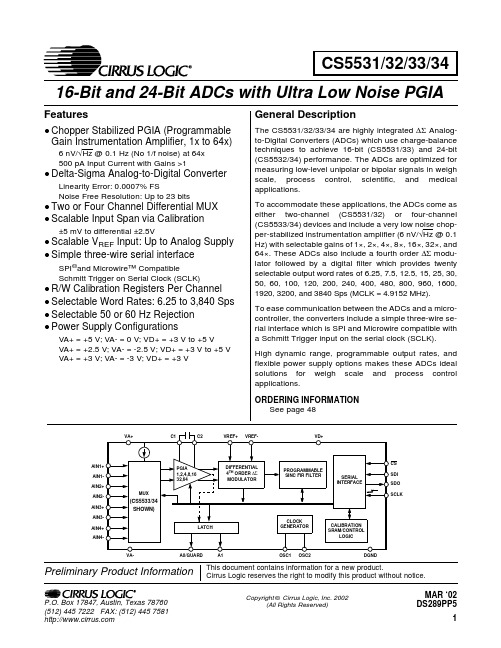
Copyright ©Cirrus Logic,Inc.200278760CS5531/32/33/3416-Bit and 24-Bit ADCs with Ultra Low Noise PGIAMAR ‘02TABLE OF CONTENTS1.CHARACTERISTICS AND SPECIFICATIONS (5)ANALOG CHARACTERISTICS (5)TYPICAL RMS NOISE(NV),CS5531/32/33/34-AS (8)TYPICAL NOISE FREE RESOLUTION(BITS),CS5532/34-AS (8)TYPICAL RMS NOISE(NV),CS5532/34-BS (9)TYPICAL NOISE FREE RESOLUTION(BITS),CS5532/34-BS (9)5V DIGITAL CHARACTERISTICS (10)3V DIGITAL CHARACTERISTICS (10)DYNAMIC CHARACTERISTICS (11)ABSOLUTE MAXIMUM RATINGS (11)SWITCHING CHARACTERISTICS (12)2.GENERAL DESCRIPTION (14)2.1.Analog Input (14)2.1.1.Analog Input Span (15)2.1.2.Multiplexed Settling Limitations (15)2.1.3.Voltage Noise Density Performance (15)2.1.4.No Offset DAC (15)2.2.Overview of ADC Register Structure and Operating Modes (16)2.2.1.System Initialization (17)mand Register Quick Reference (19)mand Register Descriptions (20)2.2.4.Serial Port Interface (24)2.2.5.Reading/Writing On-Chip Registers (25)2.3.Configuration Register (25)2.3.1.Power Consumption (25)2.3.2.System Reset Sequence (25)2.3.3.Input Short (26)2.3.4.Guard Signal (26)2.3.5.Voltage Reference Select (26)2.3.6.Output Latch Pins (26)2.3.7.Offset and Gain Select (27)Contacting Cirrus Logic SupportFor a complete listing of Direct Sales,Distributor,and Sales Representative contacts,visit the Cirrus Logic web site at: /corporate/contacts/sales.cfmSPI is a registered trademark of International Business Machines Corporation.Microwire is a trademark of National Semiconductor Corporation.IMPORTANT NOTICE"Preliminary"product information describes products that are in production,but for which full characterization data is not yet available."Advance"product infor-mation describes products that are in development and subject to development changes.Cirrus Logic,Inc.and its subsidiaries("Cirrus")believe that the infor-mation contained in this document is accurate and reliable.However,the information is subject to change without notice and is provided"AS IS"without warranty of any kind(express or implied).Customers are advised to obtain the latest version of relevant information to verify,before placing orders,that information being relied on is current and complete.All products are sold subject to the terms and conditions of sale supplied at the time of order acknowledgment,including those pertaining to warranty,patent infringement,and limitation of liability.No responsibility is assumed by Cirrus for the use of this information,including use of this information as the basis for manufacture or sale of any items,or for infringement of patents or other rights of third parties.This document is the property of Cirrus and by furnishing this information,Cirrus grants no license,express or implied under any patents,mask work rights,copyrights,trademarks,trade secrets or other intellectual property rights.Cirrus owns the copyrights of the information contained herein and gives consent for copies to be made of the information only for use within your organization with respect to Cirrus integrated circuits or other parts of Cirrus.This consent does not extend to other copying such as copying for general distribution,advertising or promotional purposes,or for creating any work for resale.An export permit needs to be obtained from the competent authorities of the Japanese Government if any of the products or technologies described in this ma-terial and controlled under the"Foreign Exchange and Foreign Trade Law"is to be exported or taken out of Japan.An export license and/or quota needs to be obtained from the competent authorities of the Chinese Government if any of the products or technologies described in this material is subject to the PRC Foreign Trade Law and is to be exported or taken out of the PRC.CERTAIN APPLICATIONS USING SEMICONDUCTOR PRODUCTS MAY INVOLVE POTENTIAL RISKS OF DEATH,PERSONAL INJURY,OR SEVERE PROPERTY OR ENVIRONMENTAL DAMAGE("CRITICAL APPLICATIONS").CIRRUS PRODUCTS ARE NOT DESIGNED,AUTHORIZED,OR WARRANT-ED TO BE SUITABLE FOR USE IN LIFE-SUPPORT DEVICES OR SYSTEMS OR OTHER CRITICAL APPLICATIONS.INCLUSION OF CIRRUS PRODUCTS IN SUCH APPLICATIONS IS UNDERSTOOD TO BE FULLY AT THE CUSTOMER'S RISK.Cirrus Logic,Cirrus,and the Cirrus Logic logo designs are trademarks of Cirrus Logic,Inc.All other brand and product names in this document may be trade-marks or service marks of their respective owners.2.3.8.Filter Rate Select (27)2.3.9.Configuration Register Descriptions (28)2.4.Setting up the CSRs for a Measurement (29)2.4.1.Channel-Setup Register Descriptions (30)2.5.Calibration (32)2.5.1.Calibration Registers (32)2.5.2.Gain Register (32)2.5.3.Offset Register (32)2.5.4.Performing Calibrations (33)2.5.5.Self Calibration (33)2.5.6.System Calibration (34)2.5.7.Calibration Tips (34)2.5.8.Limitations in Calibration Range (35)2.6.Performing Conversions (35)2.6.1.Single Conversion Mode (35)2.6.2.Continuous Conversion Mode (36)2.6.3.Examples of Using CSRs to Perform Conversions and Calibrations (37)ing Multiple ADCs Synchronously (38)2.8.Conversion Output Coding (38)2.8.1.Conversion Data Output Descriptions (39)2.9.Digital Filter (40)2.10.Clock Generator (41)2.11.Power Supply Arrangements (41)2.12.Getting Started (45)2.13.PCB Layout (45)3.PIN DESCRIPTIONS (46)Clock Generator (46)Control Pins and Serial Data I/O (46)Measurement and Reference Inputs (47)Power Supply Connections (47)4.SPECIFICATION DEFINITIONS (48)5.ORDERING GUIDE (48)6.PACKAGE DRAWINGS (49)LIST OF FIGURESFigure1.SDI Write Timing(Not to Scale) (13)Figure2.SDO Read Timing(Not to Scale) (13)Figure3.Multiplexer Configuration (14)Figure4.Input models for AIN+and AIN-pins (15)Figure5.Measured Voltage Noise Density (15)Figure6.CS5531/32/33/34Register Diagram (16)mand and Data Word Timing (24)Figure8.Guard Signal Shielding Scheme (26)Figure9.Input Reference Model when VRS=1 (27)Figure10.Input Reference Model when VRS=0 (27)Figure11.Self Calibration of Offset (34)Figure12.Self Calibration of Gain (34)Figure13.System Calibration of Offset (34)Figure14.System Calibration of Gain (34)Figure15.Synchronizing Multiple ADCs (38)Figure16.Digital Filter Response(Word Rate=60Sps) (40)Figure17.120Sps Filter Magnitude Plot to120Hz (40)Figure18.120Sps Filter Phase Plot to120Hz (40)Figure19.Z-Transforms of Digital Filters (40)Figure20.On-chip Oscillator Model (41)Figure21.CS5532Configured with a Single+5V Supply (42)Figure22.CS5532Configured with±2.5V Analog Supplies (43)Figure23.CS5532Configured with±3V Analog Supplies (43)Figure24.CS5532Configured for Thermocouple Measurement (44)Figure25.Bridge with Series Resistors (44)LIST OF TABLESTable1.Conversion Timing for Single Mode (36)Table2.Conversion Timing for Continuous Mode (37)mand Byte Pointer (37)Table4.Output Coding for16-bit CS5531and CS5533 (39)Table5.Output Coding for24-bit CS5532and CS5534 (39)1.CHARACTERISTICS AND SPECIFICATIONSANALOG CHARACTERISTICS(VA+,VD+=5V ±5%;VREF+=5V;VA-,VREF-,DGND =0V;MCLK =4.9152MHz;OWR (Output Word Rate)=60Sps;Bipolar Mode;Gain =32)(See Notes 1and 2.)Notes: 1.Applies after system calibration at any temperature within -40°C ~+85°C.2.Specifications guaranteed by design,characterization,and/or test.LSB is 16bits for the CS5531/33andLSB is 24bits for the CS5532/34.3.This specification applies to the device only and does not include any effects by external parasiticthermocouples.The PGIA contributes 5nV of offset drift,and the modulator contributes 640/G nV of offset drift,where G is the amplifier gain setting.4.Drift over specified temperature range after calibration at power-up at 25°C.ParameterCS5531-AS/CS5533-ASUnit Min Typ Max Accuracy Linearity Error -±0.0015±0.003%FS No Missing Codes 16--Bits Bipolar Offset -±1±2LSB 16Unipolar Offset-±2±4LSB 16Offset Drift(Notes 3and 4)-640/G +5-nV/°C Bipolar Full Scale Error -±8±31ppm Unipolar Full Scale Error -±16±62ppm Full Scale Drift(Note 4)-2-ppm/°CParameterCS5532-AS/CS5534-ASCS5532-BS/CS5534-BS Unit Min Typ Max Min Typ Max Accuracy Linearity Error -±0.0015±0.003-±0.0007±0.0015%FS No Missing Codes 24--24--Bits Bipolar Offset -±16±32-±16±32LSB 24Unipolar Offset-±32±64-±32±64LSB 24Offset Drift(Notes 3and 4)-640/G +5--640/G +5-nV/°C Bipolar Full Scale Error -±8±31-±8±31ppm Unipolar Full Scale Error -±16±62-±16±62ppm Full Scale Drift(Note 4)-TBD--2-ppm/°CANALOG CHARACTERISTICS(Continued)(See Notes 1and 2.)Notes: 5.The voltage on the analog inputs is amplified by the PGIA,and becomes V CM ±Gain*(AIN+-AIN-)/2atthe differential outputs of the amplifier.In addition to the input common mode +signal requirements for the analog input pins,the differential outputs of the amplifier must remain between (VA-+0.1V)and (VA+-0.1V)to avoid saturation of the output stage.6.See the section of the data sheet which discusses input models.ParameterMinTypMaxUnitAnalog InputCommon Mode +Signal on AIN+or AIN-Bipolar/Unipolar ModeGain =1Gain =2,4,8,16,32,64(Note 5)VA-VA-+0.7--VA+VA+-1.7V V CVF Current on AIN+or AIN-Gain =1(Note 6)Gain =2,4,8,16,32,64--500500--nA pA Input Current Noise Gain =1Gain =2,4,8,16,32,64--2001--pA/√Hz pA/√Hz Input Leakage for Mux when Off (at 25°C)-10-pA Off-Channel Mux Isolation -120-dB Open Circuit Detect Current 100300-nA Common Mode Rejection dc,Gain =1dc,Gain =6450,60Hz ---90130120---dB dB dB Input Capacitance -60-pF Guard Drive Output -20-µA Voltage Reference Input Range (VREF+)-(VREF-)1 2.5(VA+)-(VA-)V CVF Current (Note 6)-500-nA Common Mode Rejection dc 50,60Hz --120120--dB dB Input Capacitance 11-22pF System Calibration Specifications Full Scale Calibration Range Bipolar/Unipolar Mode 3-110%FS Offset Calibration Range Bipolar Mode -100-100%FS Offset Calibration Range Unipolar Mode -90-90%FSANALOG CHARACTERISTICS(Continued)(See Notes 1and 2.)7.All outputs unloaded.All input CMOS levels.8.Power is specified when the instrumentation amplifier (Gain ≥2)is on.Analog supply current is reducedby approximately 1/2when the instrumentation amplifier is off (Gain =1).9.Tested with 100mV change on VA+or VA-.ParameterCS5531/32/33/34-AS CS5532/34-BS MinTypMaxMinTypMaxUnitPower SuppliesDC Power Supply Currents (Normal Mode)I A+,I A-I D+--60.581--130.5151mA mA Power ConsumptionNormal Mode (Notes 7and 8)Standby Sleep---35350045-----70450080--mW mW µW Power Supply Rejection(Note 9)dc Positive Supplies dc Negative Supply--115115----115115--dB dBTYPICAL RMS NOISE (nV),CS5531/32/33/34-AS (See notes 10,11and 12)Notes:10.Wideband noise aliased into the baseband.Referred to the input.Typical values shown for 25°C.11.For Peak-to-Peak Noise multiply by 6.6for all ranges and output rates.12.Word rates and -3dB points with FRS =0.When FRS =1,word rates and -3dB points scale by 5/6.TYPICAL NOISE FREE RESOLUTION(BITS),CS5532/34-AS (See Notes 13and 14)13.Noise Free Resolution listed is for Bipolar operation,and is calculated as LOG((Input Span)/(6.6xRMSNoise))/LOG(2)rounded to the nearest bit.For Unipolar operation,the input span is 1/2as large,so one bit is lost.The input span is calculated in the analog input span section of the data sheet.The Noise Free Resolution table is computed with a value of 1.0in the gain register.Values other than 1.0will scale the noise,and change the Noise Free Resolution accordingly.14.“Noise Free Resolution”is not the same as “Effective Resolution”.Effective Resolution is based on theRMS noise value,while Noise Free Resolution is based on a peak-to-peak noise value specified as 6.6times the RMS noise value.Effective Resolution is calculated as LOG((Input Span)/(RMS Noise))/LOG(2).Specifications are subject to change without notice.Output Word Rate (Sps)-3dB Filter Frequency (Hz)Instrumentation Amplifier Gain x64x32x16x8x4x2x17.5 1.9417171926427915515 3.882425273659111218307.7534353951841573086015.548495472118222436120316870771021673146162406211516027652710402070415048012216323039274814802950589096023022932155410602090417083401,920390344523946184036507290146003,84078013902710539010800215004300086100Output Word Rate (Sps)-3dB Filter Frequency (Hz)Instrumentation Amplifier Gain x64x32x16x8x4x2x17.5 1.941920212222222215 3.8819202121212222307.75181920212121216015.5181920202021211203117181920202020240621617171717171748012216171717171717960230151616161616161,920390151515151515153,84078013131313131313TYPICAL RMS NOISE (nV),CS5532/34-BS (See notes 15,16,17and 18)Notes:15.The -B devices provide the best noise specifications.16.Wideband noise aliased into the baseband.Referred to the input.Typical values shown for 25°C.17.For Peak-to-Peak Noise multiply by 6.6for all ranges and output rates.18.Word rates and -3dB points with FRS =0.When FRS =1,word rates and -3dB points scale by 5/6.TYPICAL NOISE FREE RESOLUTION(BITS),CS5532/34-BS (See Notes 19and 20)19.Noise Free Resolution listed is for Bipolar operation,and is calculated as LOG((Input Span)/(6.6xRMSNoise))/LOG(2)rounded to the nearest bit.For Unipolar operation,the input span is 1/2as large,so one bit is lost.The input span is calculated in the analog input span section of the data sheet.The Noise Free Resolution table is computed with a value of 1.0in the gain register.Values other than 1.0will scale the noise,and change the Noise Free Resolution accordingly.20.“Noise Free Resolution”is not the same as “Effective Resolution”.Effective Resolution is based on theRMS noise value,while Noise Free Resolution is based on a peak-to-peak noise value specified as 6.6times the RMS noise value.Effective Resolution is calculated as LOG((Input Span)/(RMS Noise))/LOG(2).Specifications are subject to change without notice.Output Word Rate (Sps)-3dB Filter Frequency (Hz)Instrumentation Amplifier Gain x64x32x16x8x4x2x17.5 1.948.59101526509915 3.88121315213770139307.751718213052991966015.524252942731402771203134364259103198392240628013626051410202050409048012211319436973014502900581096023015927452310302060411082301,920390260470912181036207230145003,84078013602690538010800215004300086000Output Word Rate (Sps)-3dB Filter Frequency (Hz)Instrumentation Amplifier Gain x64x32x16x8x4x2x17.5 1.942021222323232315 3.8820212222222222307.75192021222222226015.5192021212121211203118192021212121240621717181818181848012217171717171717960230161617171717171,920390161616161616163,840780131313131313135V DIGITAL CHARACTERISTICS (VA+,VD+=5V ±5%;VA-,DGND =0V;See Notes 2and 21.)3V DIGITAL CHARACTERISTICS (T A =25°C;VA+=5V ±5%;VD+=3.0V±10%;VA-,DGND =0V;See Notes 2and 21.)21.All measurements performed under static conditions.ParameterSymbol Min Typ Max Unit High-Level Input Voltage All Pins Except SCLKSCLK V IH 0.6VD+(VD+)-0.45--VD+VD+V Low-Level Input Voltage All Pins Except SCLKSCLK V IL 0.00.0-0.80.6V High-Level Output Voltage A0and A1,I out =-1.0mASDO,I out =-5.0mA V OH (VA+)-1.0(VD+)-1.0--V Low-Level Output Voltage A0and A1,I out =1.0mASDO,I out =5.0mAV OL --(VA-)+0.40.4V Input Leakage Current I in -±1±10µA SDO 3-State Leakage Current I OZ --±10µA Digital Output Pin CapacitanceC out-9-pFParameterSymbol Min Typ Max Unit High-Level Input Voltage All Pins Except SCLKSCLK V IH 0.6VD+(VD+)-0.45-VD+VD+V Low-Level Input Voltage All Pins Except SCLKSCLK V IL 0.00.0-0.80.6V High-Level Output Voltage A0and A1,I out =-1.0mASDO,I out =-5.0mA V OH (VA+)-1.0(VD+)-1.0--V Low-Level Output Voltage A0and A1,I out =1.0mASDO,I out =5.0mAV OL --(VA-)+0.40.4V Input Leakage Current I in -±1±10µA SDO 3-State Leakage Current I OZ --±10µA Digital Output Pin CapacitanceC out-9-pFDYNAMIC CHARACTERISTICS22.The ADCs use a Sinc 5filter for the 3200Sps and 3840Sps output word rate (OWR)and a Sinc 5filterfollowed by a Sinc 3filter for the other OWRs.OWR sinc5refers to the 3200Sps (FRS =1)or 3840Sps (FRS =0)word rate associated with the Sinc 5filter.23.The single conversion mode only outputs fully settled conversions.See Table 1for more details aboutsingle conversion mode timing.OWR SC is used here to designate the different conversion time associated with single conversions.24.The continuous conversion mode outputs every conversion.This means that the filter’s settling timewith a full scale step input in the continuous conversion mode is dictated by the OWR.ABSOLUTE MAXIMUM RATINGS(DGND =0V;See Note 25.)Notes:25.All voltages with respect to ground.26.VA+and VA-must satisfy {(VA+)-(VA-)}≤+6.6V.27.VD+and VA-must satisfy {(VD+)-(VA-)}≤ +7.5V.28.Applies to all pins including continuous overvoltage conditions at the analog input (AIN)pins.29.Transient current of up to 100mA will not cause SCR latch-up.Maximum input current for a power supply pin is ±50mA.30.Total power dissipation,including all input currents and output currents.WARNING:Operation at or beyond these limits may result in permanent damage to the device.Normal operation is not guaranteed at these extremes.ParameterSymbol Ratio Unit Modulator Sampling Ratef s MCLK/16Sps Filter Settling Time to 1/2LSB (Full Scale Step Input)Single Conversion mode (Notes 22,23,and 24)Continuous Conversion mode,OWR <3200Sps Continuous Conversion mode,OWR ≥3200Spst s t s t s1/OWR SC5/OWR sinc5+3/OWR5/OWRs s sParameterSymbolMin Typ Max Unit DC Power Supplies(Notes 26and 27)Positive Digital Positive Analog Negative Analog VD+VA+VA--0.3-0.3+0.3---+6.0+6.0-3.75V V V Input Current,Any Pin Except Supplies (Notes 28and 29)I IN --±10mA Output Current I OUT --±25mA Power Dissipation (Note 30)PDN --500mW Analog Input Voltage VREF pins AIN PinsV INR V INA (VA-)-0.3(VA-)-0.3--(VA+)+0.3(VA+)+0.3V V Digital Input VoltageV IND -0.3-(VD+)+0.3V Ambient Operating Temperature T A -40-85°C Storage T emperature T stg-65-150°CSWITCHING CHARACTERISTICS (VA+=2.5V or 5V ±5%;VA-=-2.5V±5%or 0V;VD+=3.0V±10%or 5V ±5%;DGND =0V;Levels:Logic 0=0V,Logic 1=VD+;C L =50pF;See Figures 1and 2.)Notes:31.Device parameters are specified with a 4.9152MHz clock.32.Specified using 10%and 90%points on waveform of interest.Output loaded with 50pF.33.Oscillator start-up time varies with crystal parameters.This specification does not apply when using anexternal clock source.ParameterSymbol MinTypMaxUnitMaster Clock Frequency (Note 31)External Clock or Crystal OscillatorMCLK1 4.91525MHz Master Clock Duty Cycle 40-60%Rise Times(Note 32)Any Digital Input Except SCLKSCLKAny Digital Output t rise-----50 1.0100-µs µs ns Fall Times(Note 32)Any Digital Input Except SCLKSCLKAny Digital Output t fall-----50 1.0100-µs µs ns Start-upOscillator Start-up Time XTAL =4.9152MHz(Note 33)t ost-20-ms Serial Port Timing Serial Clock Frequency SCLK 0-2MHz Serial Clock Pulse Width High Pulse Width Lowt 1t 2250250----ns nsSDI Write TimingCS Enable to Valid Latch Clock t 350--ns Data Set-up Time prior to SCLK rising t 450--ns Data Hold Time After SCLK Rising t 5100--ns SCLK Falling Prior to CS Disable t 6100--nsSDO Read Timing CS to Data Validt 7--150ns SCLK Falling to New Data Bit t 8--150ns CS Rising to SDO Hi-Zt 9--150nsFigure1.SDI Write Timing(Not toScale)2.GENERAL DESCRIPTIONThe CS5531/32/33/34are highly integrated∆ΣAn-alog-to-Digital Converters(ADCs)which use charge-balance techniques to achieve16-bit (CS5531/33)and24-bit(CS5532/34)performance. The ADCs are optimized for measuring low-level unipolar or bipolar signals in weigh scale,process control,scientific,and medical applications.To accommodate these applications,the ADCs come as either two-channel(CS5531/32)or four-channel(CS5533/34)devices and include a very low noise chopper-stabilized programmable gain instrumentation amplifier(PGIA,6nV/√Hz@0.1 Hz)with selectable gains of1×,2×,4×,8×,16×, 32×,and64×.These ADCs also include a fourth or-der∆Σmodulator followed by a digital filter which provides twenty selectable output word rates of6.25, 7.5,12.5,15,25,30,50,60,100,120,200,240,400, 480,800,960,1600,1920,3200,and3840Samples per second(MCLK=4.9152MHz).To ease communication between the ADCs and a micro-controller,the converters include a simple three-wire serial interface which is SPI and Mi-crowire compatible with a Schmitt Trigger input on the serial clock(SCLK).2.1.Analog InputFigure3illustrates a block diagram of the CS5531/32/33/34.The front end consists of a multi-plexer,a unity gain coarse/fine charge input buffer, and a programmable gain chopper-stabilized instru-mentation amplifier.The unity gain buffer is activat-ed any time conversions are performed with a gain of one and the instrumentation amplifier is activated any time conversions are performed with gain set-tings greater than one.The unity gain buffer is designed to accommodate rail to rail input signals.The common-mode plus signal range for the unity gain buffer amplifier is VA-to VA+.Typical CVF(sampling)current for the unity gain buffer amplifier is about500nA (MCLK=4.9152MHz,see Figure4).The instrumentation amplifier is chopper-stabi-lized and operates with a chop clock frequency of MCLK/128.The CVF(sampling)current into the instrumentation amplifier is typically500pA overFigure3.Multiplexer Configuration-40°C to+85°C(MCLK=4.9152MHz).The com-mon-mode plus signal range of the instrumentation amplifier is(VA-)+0.7V to(VA+)-1.7V. Figure4illustrates the input models for the ampli-fiers.The dynamic input current for each of the pins can be determined from the models shown. Note:The C=2.5pF and C=16pF capacitors are for input current modeling only.For physicalinput capacitance see‘Input Capacitance’specification under Analog Characteristics.2.1.1.Analog Input SpanThe full scale input signal that the converter can dig-itize is a function of the gain setting and the refer-ence voltage connected between the VREF+and VREF-pins.The full scale input span of the convert-er is((VREF+)-(VREF-))/(GxA),where G is the gain of the amplifier and A is2for VRS=0,or A is 1for VRS=1.VRS is the Voltage Reference Select bit,and must be set according to the differential volt-age applied to the VREF+and VREF-pins on the part.See section2.3.5for more details.After reset,the unity gain buffer is engaged.With a 2.5V reference this would make the full scale input range default to2.5V.By activating the instrumen-tation amplifier(i.e.a gain setting other than1)and using a gain setting of32,the full scale input range can quickly be set to2.5/32or about78mV.Note that these input ranges assume the calibration regis-ters are set to their default values(i.e.Gain=1.0and Offset=0.0).2.1.2.Multiplexed Settling LimitationsThe settling performance of the CS5531/32/33/34 in multiplexed applications is affected by the sin-gle-pole low-pass filter which follows the instru-mentation amplifier(see Figure3).To achieve data sheet settling and linearity specifications,it is rec-ommended that a22nF C0G capacitor be used.Ca-pacitors as low as10nF or X7R type capacitors can also be used with some minor increase in distortion for AC signals.2.1.3.Voltage Noise Density Performance Figure5illustrates the measured voltage noise den-sity versus frequency from0.01Hz to10Hz of a CS5532-BS.The device was powered with±2.5V supplies,using120Sps OWR,the64x gain range, bipolar mode,and with the input short bit enabled.2.1.4.No Offset DACAn offset DAC was not included in the CS553X family because the high dynamic range of the con-verter eliminates the need for one.The offset regis-Figure4.Input models for AIN+and AIN-pinster can be manipulated by the user to mimic the function of a DAC if desired.2.2.Overview of ADC Register Structure and Operating ModesThe CS5531/32/33/34ADCs have an on-chip con-troller,which includes a number of user-accessible registers.The registers are used to hold offset and gain calibration results,configure the chip's operat-ing modes,hold conversion instructions,and to store conversion data words.Figure6depicts a block diagram of the on-chip controller’s internal registers.Each of the converters has32-bit registers to func-tion as offset and gain calibration registers for each channel.The converters with two channels have two offset and two gain calibration registers,the converters with four channels have four offset and four gain calibration registers.These registers hold calibration results.The contents of these registers can be read or written by the user.This allows cal-ibration data to be off-loaded into an external EE-PROM.The user can also manipulate the contents of these registers to modify the offset or the gain slope of the converter.The converters include a32-bit configuration reg-ister which is used for setting options such as the power down modes,resetting the converter,short-ing the analog inputs,and enabling diagnostic test bits like the guard signal.A group of registers,called Channel Setup Regis-ters,are used to hold pre-loaded conversion in-structions.Each channel setup register is32bits long,and holds two16-bit conversion instructions referred to as Setups.Upon power up,these regis-ters can be initialized by the system microcontrol-ler with conversion instructions.The user can then instruct the converter to perform single or multiple conversions or calibrations with the converter in the mode defined by one of these Setups.Figure6.CS5531/32/33/34Register DiagramUsing the single conversion mode,an8-bit com-mand word can be written into the serial port.The command includes pointer bits which‘point’to a 16-bit command in one of the Channel Setup Reg-isters which is to be executed.The16-bit Setups can be programmed to perform a conversion on any of the input channels of the converter.More than one of the16-bit Setups can be used for the same analog input channel.This allows the user to con-vert on the same signal with either a different con-version speed,a different gain range,or any of the other options available in the channel setup regis-ters.Alternately,the user can set up the registers to perform different conversion conditions on each of the input channels.The ADCs also include continuous conversion ca-pability.The ADCs can be instructed to continu-ously convert,referencing one16-bit command Setup.In the continuous conversions mode,the conversion data words are loaded into a shift regis-ter.The converter issues a flag on the SDO pin when a conversion cycle is completed so the user can read the register,if need be.See the section on Performing Conversions for more details.The following pages document how to initialize the converter,perform offset and gain calibrations,and how to configure the converter for the various con-version modes.Each of the bits of the configuration register and of the Channel Setup Registers is de-scribed.A list of examples follows the description section.Also the Command Register Quick Refer-ence can be used to decode all valid commands(the first8-bits into the serial port).2.2.1.System InitializationThe CS5531/32/33/34provide no power-on-reset function.To initialize the ADCs,the user must per-form a software reset by resetting the ADC’s serial port with the Serial Port Initialization sequence. This sequence resets the serial port to the command mode and is accomplished by transmitting at least 15SYNC1command bytes(0xFF hexadecimal),followed by one SYNC0command(0xFE hexa-decimal).Note that this sequence can be initiated at anytime to reinitialize the serial port.To complete the system initialization sequence,the user must also perform a system reset sequence which is as follows:Write a logic1into the RS bit of the con-figuration register.This will reset the calibration registers and other logic(but not the serial port).A valid reset will set the RV bit in the configuration register to a logic1.After writing the RS bit to a logic1,wait20microseconds,then write the RS bit back to logic0.While this involves writing an en-tire word into the configuration register,the RV bit is a read only bit,therefore a write to the configu-ration register will not overwrite the RV bit.After clearing the RS bit back to logic0,read the config-uration register to check the state of the RV bit as this indicates that a valid reset occurred.Reading the configuration register clears the RV bit back to logic0.Completing the reset cycle initializes the on-chip registers to the following states:Note:Previous datasheets stated that the RS bit would clear itself back to logic0and thereforethe user was not required to write the RS bitback to logic0.The current data sheetinstruction that requires the user to write intothe configuration register to clear the RS bithas been added to insure that the RS bit iscleared.Characterization across multiple lotsof silicon has indicated some chips do notautomatically reset the RS bit to logic0in theconfiguration register,although the resetfunction is completed.This occurs only onsmall number of chips when the VA-supply isnegative with respect to DGND.This has notcaused an operational issue for customersbecause their start-up sequence includeswriting a word(with RS=0)into theconfiguration register after performing areset.The change in the reset sequence to Configuration Register:00000000(H)Offset Registers:00000000(H)Gain Registers:01000000(H)Channel Setup Registers:00000000(H)。
汤诚产品主推型号2015年12月9日-V 1.0

5000mA
Power Switch(电源限流开关 ☆☆☆ ☆ ☆☆☆☆ TCS9208_V3.0 TCS3354_V1.0 TCS3358_V1.0 稳定 屏偏压 屏偏压 2.6-6.0 2.5-5.5 2.5-5.5 1500mA 28(ADJ) 28(ADJ)
LDO(线性稳压器 ) 推荐等级 ☆ 产品型号 TCS2165_V2.0 TCS2163 V2.0 特点 高精度最低成本 高精度最低成本 工作电压(V) 1.8-5.0 1.8-5.0 输出电流(V) 250mA 250mA
充电电流 1.0A 1.0A 1.2A 1.5A 2.0A 1.0A 1.2A 2.1A
放电电流 1.0A 1.0A 1.0A 2A(MAX) 2.0A 2A 1.2A 2.1A
LED灯颗数 1、2 三色 1、2、3、4 3、4、5 3、4、5 3、4、5 3、4、5 3、4、5
☆☆☆☆ ☆☆☆☆
PC9103 PC9305 PC9206
Precision Measurement Un 功能模块 HV BUCK1 HV BUCK2 LV BUCK1 PC6592 LV BUCK2 WLED LDO1 LDO2 Power On Reset 功能模块 HV BUCK1 HV BUCK2 LV BUCK1 PC6591 LV BUCK2 WLED LDO1 输入电压 4.5~17V 4.5~17V 2.5V-5.5V 2.5V-5.5V 4.5~17V 2.5V-5.5V 2.5V-5.5V / 输入电压 3.6V~18V 3.6V~18V 2.5V-5.5V 2.5V-5.5V 2.5~5.5V 2.5V-5.5V 1.2/1.5/1.8/3.3 输出电压 ADJ ADJ ADJ ADJ ADJ 3.3V ADJ Open Drain 输出电压 1.2/3.3/5/ADJ 1.2/3.3/5/ADJ 1.2/1.1/1.35/ADJ 1.2/1.5/1.8/ADJ
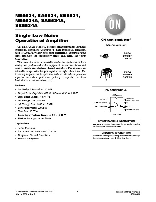
NE5534_中文资料
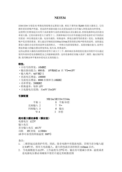
NE55345533/5534分别是双/单路高效低噪音运算放大器。
相比于那些如TL083的放大器而言,它们拥有更好的噪声性能,更高的外部驱动能力以及更加高的小信号输入和更高的功率带宽。
这使得它们特别适合应用于高质量和专业的音频设备以及仪器仪表,控制电路和电话信道功率放大器。
它的内部补偿大于或等于三,其频率响应可以在外部通过补偿电容针对不同的应用需求(单位增益放大器,电容负载性,转换速率,降低自激等等的要求)优化。
如果超低噪声是首要的要求,那么建议仔细阅读5533A/5534A类型的保证噪声特性的说明。
高性能运算放大器结合良好的直流和交流的特点。
一些特点包括很低噪音、高驱动输出能力,高单位增益和最大的输出摆动带宽和高,低失真,转换速率。
这些运算放大器的内部得到补偿等于或大于三个。
频率响应各种的优化使应用程序可以通过使用外部补偿电容器赔偿金之间能够被获得。
这些设备特征有输入保护二极管、输出保护短路,使用剩余和平衡来补偿电压无效的能力。
特性:·小信号的带宽:10MHZ·输出驱动能力:600 Ω,10VRMS at 在VS=±18V·输入噪声:4nV/HZ^2·直流电压增益:100000·交流电压增益:6000在频率为10KHZ·功率带宽:200KHZ·转换速率:每秒13V·大电源电压范围:从±3V到±20V引脚配置NE/SA/SE5534/5534A平衡1 8 平衡/补偿反相输入2 7 V+同相输入 3 6 输出V- 4 5 补偿绝对最大额定参数(额定值)电源电压 ±22V输入电压差分输入电压 ±0.5V功耗8N封装1150Mw10秒可承受的焊接温度300︒C备注:1.二极管起过流保护作用,因此,除非电路中有限流电阻,否则当差分输入超过0.6V时,将有大电流输入。
最大的电流应该控制在 ±10mA以内。
常用运放 稳压等芯片简介
型号资料名称4N35/4N36/4N37光电耦合器AD7520/AD7521/AD7530/AD7521D/A转换器AD754112位D/A转换器ADC0802/ADC0803/ADC08048位A/D转换器ADC0808/ADC08098位A/D转换器ADC0831/ADC0832/ADC0834/ADC08388位A/D转换器CA3080/CA3080A OTA跨导运算放大器CA3140/CA3140A BiMOS运算放大器DAC0830/DAC08328位D/A转换器ICL7106,ICL71073位半A/D转换器ICL7116,ICL71173位半A/D转换器ICL7650载波稳零运算放大器ICL7660/MAX1044CMOS电源电压变换器ICL8038单片函数发生器ICM721610MHz通用计数器ICM7226带BCD输出10MHz通用计数器ICM7555/7555CMOS单/双通用定时器ISO2-CMOS MT8880C DTMF收发器LF351JFET输入运算放大器LF353JFET输入宽带高速双运算放大器 LM117/LM317A/LM317三端可调电源LM124/LM124/LM324低功耗四运算放大器LM137/LM337三端可调负电压调整器LM139/LM239/LM339低功耗四电压比较器LM158/LM258/LM358低功耗双运算放大器LM193/LM293/LM393低功耗双电压比较器LM201/LM301通用运算放大器LM231/LM331精密电压—频率转换器LM285/LM385微功耗基准电压二极管LM308A精密运算放大器LM386低压音频小功率放大器LM399带温度稳定器精密电压基准电路LM431可调电压基准电路LM567/LM567C锁相环音频译码器LM741运算放大器LM831双低噪声音频功率放大器LM833双低噪声音频放大器LM8365双定时LED电子钟电路MAX0380.1Hz-20MHz单片函数发生器MAX2325V电源多通道RS232驱动器/接收器MC1403 2.5V精密电压基准电路MC1404 5.0v/6.25v/10v基准电压MC1413/MC1416七路达林顿驱动器MC145026/MC145027/MC145028编码器/译码器MC145403-5/8RS232驱动器/接收器MC145406RS232驱动器/接收器MC145407RS232驱动器/接收器MC145583RS232驱动器/接收器MC145740DTMF接收器MC1488二输入与非四线路驱动器MC1489四施密特可控线路驱动器MC2833低功率调频发射系统MC3362低功率调频窄频带接收器MC4558双运算放大器MC7800系列 1.0A三端正电压稳压器MC78L00系列0.1A三端正电压稳压器MC78M00系列0.5A三端正电压稳压器MC78T00系列 3.0A正电压稳压器MC7900系列 1.0A三端负电压稳压器MC79L00系列0.1A三端负电压稳压器MC79M00系列0.5A三端负电压稳压器Microchip PIC系列单片机RS232通讯应用MM5369 3.579545MHz-60Hz 17级分频振荡器MOC3009/MOC3012双向可控硅输出光电耦合器MOC3020/MOC3023双向可控硅输出光电耦合器MOC3081/MOC3082/MOC3083过零双向可控硅输出光电耦合器MOC8050无基极达林顿晶体管输出光电耦合器 MOC8111无基极晶体管输出光电耦合器MT8870DTMF双音频接收器MT8888C DTMF 收发器NE5532/NE5532A双低噪声运算放大器NE5534/SE5534低噪声运算放大器NE555/SA555单时基电路NE556/SA556/SE556双时基电路NE570/NE571/SA571音频压缩扩展器OP07低电压飘移运算放大器OP27低噪音精密运算放大器OP37低噪音高速精密运算放大器OP77低电压飘移运算放大器OP90精密低电压微功耗运算放大器PC817/PC827/PC847高效光电耦合器PT2262无线遥控发射编码器芯片PT2272无线遥控接收解码器芯片SG2524/SG3524脉宽调制PWMST7537电力线调制解调器电路TDA15212×12W Hi-Fi 音频功率放大器 TDA203014W Hi-Fi 音频功率放大器TDA26162×12W Hi-Fi 音频功率放大器TDA7000T FM 单片调频接收电路TDA7010T FM 单片调频接收电路TDA7021T FM MTS单片调频接收电路TDA7040T低电压锁相环立体声解码器TDA7050低电压单/双声道功率放大器TL062/TL064低功耗JFET输入运算放大器TL071/TL072/TL074低噪声JFET输入运算放大器TL082/TL084JFET 宽带高速运算放大器TL494脉宽调制PWMTL594精密开关模式脉宽调制控制TLP521/1-4光电耦合器TOP100-4TOPSwitch 三端PWM开关电源电路TOP200-4TOPSwitch 三端PWM开关电源电路TOP209/TOP210TOPSwitch 三端PWM开关电源电路TOP221-7TOPSwitch-Ⅱ 三端PWM开关电源电路TOP232-4TOPSwitch-FX 五端柔韧设计开关电源电路 TOP412/TOP414TOPSwitch 三端PWM DC-DC 开关电源ULN2068 1.5A/50V 4路达林顿驱动电路ULN2803500mA/50V 8路达林顿驱动电路ULN2803/ULN2804线性八外围驱动器阵列VFC32电压—频率/频率—电压转换器备注10-Bit,12-Bit,Multiplying D/A Converters12-Bit,Multiplying D/A Converter8-Bit,Microprocessor-Compatibie,A/D Converters8-Bit μP Compatibie A/D Converters with 8-Channel Multiplexer8-Bit Serial I/O A/D Converters with Multiplexer Options8-Bit μP Compatibie,Double-Buffered D to A ConvertersICL7106,ICL7107,ICL7106S,ICL7107S 3位半LCD/LED显示A/D转换器(ICL7106,ICL7107,ICL7106S,ICL7 ICL7116,ICL7117 3位半LCD/LED显示数据保持A/D转换器(ICL7116,ICL7117 ,3 1/2 Digit,LCD/LED Di ICM7216A/ICM7216B/ICM7216D 10MHz通用计数器、数字频率计、计数器、周期测量仪等仪器的单片专用ICM7226A/ICM7226B 带BCD输出10MHz通用计数器、数字频率计、计数器、周期测量仪等仪器的单片专用ICM7555/ICM7555 CMOS General Purpose TimersISO2-CMOS MT8880C Integrated DTMF TransceiverLM124/LM124/LM324/LM2902 低功耗四运算放大器LM139/LM239/LM339/LM2901/LM3302 低功耗四电压比较器LM158/LM258/LM358/LM2904 低功耗双运算放大器LM193/LM293/LM393/LM2903 低功耗双电压比较器LM231A/LM231/LM331A/LM331 精密电压—频率转换器LM199/LM299/LM399/LM3999 带温度稳定器精密电压基准电路LM741A/LM741E/LM741/LM741C 运算放大器LM8365 双定时LED电子钟电路,中文杂志扫描的PDF文件。
液晶常用电源管理芯片

1200AP40 1200AP60、1203P60200D6、203D6 DAP8A 可互代203D6/1203P6 DAP8A2S0680 2S08803S0680 3S08805S0765 DP104、DP7048S0765C DP704加24V得稳压二极管ACT4060 ZA3020LV/MP1410/MP9141ACT4065 ZA3020/MP1580ACT4070 ZA3030/MP1583/MP1591MP1593/MP1430ACT6311 LT1937ACT6906 LTC3406/A T1366/MP2104AMC2576 LM2576AMC2596 LM2596AMC3100 LTC3406/AT1366/MP2104AMC34063A AMC34063AMC7660 AJC1564AP8012 VIPer12AAP8022 VIPer22ADAP02 可用SG5841 /SG6841代换DAP02ALSZ SG6841DAP02ALSZ SG6841DAP7A、DP8A 203D6、1203P6DH321、DL321 Q100、DM0265RDM0465R DM/CM0565RDM0465R/DM0565R 用cm0565r代换(取掉4脚得稳压二极管) DP104 5S0765DP704 5S0765DP706 5S0765DP804 DP904FAN7601 LAF0001LD7552 可用SG6841代(改4脚电阻)LD7575PS 203D6改1脚100K电阻为24KOB2268CP OB2269CPOB2268CP SG6841改4脚100K电阻为2047KOCP1451 TL1451/BA9741/SP9741/AP200OCP2150 LTC3406/AT1366/MP2104OCP2160 LTC3407OCP2576 LM2576OCP3601 MB3800OCP5001 TL5001OMC2596 LM2596/AP1501PT1301 RJ9266PT4101 AJC1648/MP3202PT4102 LT1937/AJC1896/AP1522/RJ9271/MP1540SG5841SZ SG6841DZ/SG6841DSM9621 RJ9621/AJC1642SP1937 LT1937/AJC1896/AP1522/RJ9271/MP1540STRG5643D STRG5653D、STRG8653DTEA1507 TEA1533TEA1530 TEA1532对应引脚功能接入THX202H TFC719THX203H TFC718STOP246Y TOP247YV A7910 MAX1674/75 L6920 AJC1610VIPer12A VIPer22A[audio01]ICE2A165(1A/650V、31W);ICE2A265(2A/650V、52W);ICE2B0565(0、5A/650V、23W):ICE2B165(1A/650V、31W);ICE2B265(2A/650V、52W);ICE2A180(1A/800V、29W);ICE2A280(2A/800、50W)、KA5H0365R, KA5M0365R, KA5L0365R, KA5M0365RN# u) t! u1 W1 B) R, PKA5L0365RN, KA5H0380R, KA5M0380R, KA5L0380R1、KA5Q1265RF/RT(大小两种体积)、KA5Q0765、FSCQ1265RT、KACQ1265RF、FSCQ0765RT、FSCQ1565Q这就是一类得,这些型号得引脚功能全都一样,只就是输出功率不一样。
NE5534-D芯片资料
30
100
−
−
38
−
50
100
−
−
38
−
Unit mV mV mV/°C nA nA pA/°C nA nA nA/°C mA
V dB mV/V V/mV
V
kW mA
3
NE5534, SA5534, SE5534, NE5534A, SA5534A, SE5534A
RIN
Output Short Circuit Current
ISC
3. For NE5534/5534A, TMIN = 0°C, TMAX = 70°C. 4. For SA5534/5534A, TMIN = −40°C, TMAX = +85°C. 5. For SE5534/5534A, TMIN = −55°C, TMAX = +125°C.
1. Diodes protect the inputs against overvoltage. Therefore, unless current-limiting resistors are used, large currents will flow if the differential input voltage exceeds 0.6 V. Maximum current should be limited to "10 mA.
−
Overtemperature "10 "12
−
RL w 600 W;
"15 "16
−
VS = "18 V
RL w 2.0 kW
"13 "13.5
−
运放芯片NE5534

PACKAGING INFORMATIONOrderable Device Status(1)PackageType PackageDrawingPins PackageQtyEco Plan(2)Lead/Ball Finish MSL Peak Temp(3)NE5534AD ACTIVE SOIC D875Green(RoHS&no Sb/Br)CU NIPDAU Level-2-260C-1YEARNE5534ADE4ACTIVE SOIC D875Green(RoHS&no Sb/Br)CU NIPDAU Level-2-260C-1YEARNE5534ADG4ACTIVE SOIC D875Green(RoHS&no Sb/Br)CU NIPDAU Level-2-260C-1YEARNE5534ADR ACTIVE SOIC D82500Green(RoHS&no Sb/Br)CU NIPDAU Level-2-260C-1YEARNE5534ADRE4ACTIVE SOIC D82500Green(RoHS&no Sb/Br)CU NIPDAU Level-2-260C-1YEARNE5534ADRG4ACTIVE SOIC D82500Green(RoHS&no Sb/Br)CU NIPDAU Level-2-260C-1YEAR NE5534AJG OBSOLETE CDIP JG8TBD Call TI Call TINE5534AP ACTIVE PDIP P850Pb-Free(RoHS)CU NIPDAU N/A for Pkg TypeNE5534APE4ACTIVE PDIP P850Pb-Free(RoHS)CU NIPDAU N/A for Pkg TypeNE5534D ACTIVE SOIC D875Green(RoHS&no Sb/Br)CU NIPDAU Level-2-260C-1YEARNE5534DE4ACTIVE SOIC D875Green(RoHS&no Sb/Br)CU NIPDAU Level-2-260C-1YEARNE5534DG4ACTIVE SOIC D875Green(RoHS&no Sb/Br)CU NIPDAU Level-2-260C-1YEARNE5534DR ACTIVE SOIC D82500Green(RoHS&no Sb/Br)CU NIPDAU Level-2-260C-1YEARNE5534DRE4ACTIVE SOIC D82500Green(RoHS&no Sb/Br)CU NIPDAU Level-2-260C-1YEARNE5534DRG4ACTIVE SOIC D82500Green(RoHS&no Sb/Br)CU NIPDAU Level-2-260C-1YEAR NE5534IP OBSOLETE PDIP P8TBD Call TI Call TINE5534P ACTIVE PDIP P850Pb-Free(RoHS)CU NIPDAU N/A for Pkg TypeNE5534PE4ACTIVE PDIP P850Pb-Free(RoHS)CU NIPDAU N/A for Pkg TypeNE5534PSR ACTIVE SO PS82000Green(RoHS&no Sb/Br)CU NIPDAU Level-1-260C-UNLIMNE5534PSRE4ACTIVE SO PS82000Green(RoHS&no Sb/Br)CU NIPDAU Level-1-260C-UNLIMNE5534PSRG4ACTIVE SO PS82000Green(RoHS&no Sb/Br)CU NIPDAU Level-1-260C-UNLIMSA5534AD ACTIVE SOIC D875Green(RoHS&no Sb/Br)CU NIPDAU Level-2-260C-1YEARSA5534ADE4ACTIVE SOIC D875Green(RoHS&no Sb/Br)CU NIPDAU Level-2-260C-1YEARSA5534ADG4ACTIVE SOIC D875Green(RoHS&no Sb/Br)CU NIPDAU Level-2-260C-1YEARSA5534ADR ACTIVE SOIC D82500Green(RoHS&no Sb/Br)CU NIPDAU Level-2-260C-1YEARSA5534ADRE4ACTIVE SOIC D82500Green(RoHS&CU NIPDAU Level-2-260C-1YEAROrderable Device Status(1)PackageType PackageDrawingPins PackageQtyEco Plan(2)Lead/Ball Finish MSL Peak Temp(3)no Sb/Br)SA5534ADRG4ACTIVE SOIC D82500Green(RoHS&no Sb/Br)CU NIPDAU Level-2-260C-1YEARSA5534AP ACTIVE PDIP P850Pb-Free(RoHS)CU NIPDAU N/A for Pkg TypeSA5534APE4ACTIVE PDIP P850Pb-Free(RoHS)CU NIPDAU N/A for Pkg TypeSA5534D ACTIVE SOIC D875Green(RoHS&no Sb/Br)CU NIPDAU Level-2-260C-1YEARSA5534DE4ACTIVE SOIC D875Green(RoHS&no Sb/Br)CU NIPDAU Level-2-260C-1YEARSA5534DG4ACTIVE SOIC D875Green(RoHS&no Sb/Br)CU NIPDAU Level-2-260C-1YEARSA5534DR ACTIVE SOIC D82500Green(RoHS&no Sb/Br)CU NIPDAU Level-2-260C-1YEARSA5534DRE4ACTIVE SOIC D82500Green(RoHS&no Sb/Br)CU NIPDAU Level-2-260C-1YEARSA5534DRG4ACTIVE SOIC D82500Green(RoHS&no Sb/Br)CU NIPDAU Level-2-260C-1YEARSA5534P ACTIVE PDIP P850Pb-Free(RoHS)CU NIPDAU N/A for Pkg TypeSA5534PE4ACTIVE PDIP P850Pb-Free(RoHS)CU NIPDAU N/A for Pkg TypeSA5534PS ACTIVE SO PS880Green(RoHS&no Sb/Br)CU NIPDAU Level-1-260C-UNLIMSA5534PSE4ACTIVE SO PS880Green(RoHS&no Sb/Br)CU NIPDAU Level-1-260C-UNLIMSA5534PSG4ACTIVE SO PS880Green(RoHS&no Sb/Br)CU NIPDAU Level-1-260C-UNLIMSA5534PSR ACTIVE SO PS82000Green(RoHS&no Sb/Br)CU NIPDAU Level-1-260C-UNLIMSA5534PSRE4ACTIVE SO PS82000Green(RoHS&no Sb/Br)CU NIPDAU Level-1-260C-UNLIMSA5534PSRG4ACTIVE SO PS82000Green(RoHS&no Sb/Br)CU NIPDAU Level-1-260C-UNLIM(1)The marketing status values are defined as follows:ACTIVE:Product device recommended for new designs.LIFEBUY:TI has announced that the device will be discontinued,and a lifetime-buy period is in effect.NRND:Not recommended for new designs.Device is in production to support existing customers,but TI does not recommend using this part in a new design.PREVIEW:Device has been announced but is not in production.Samples may or may not be available.OBSOLETE:TI has discontinued the production of the device.(2)Eco Plan-The planned eco-friendly classification:Pb-Free(RoHS),Pb-Free(RoHS Exempt),or Green(RoHS&no Sb/Br)-please check /productcontent for the latest availability information and additional product content details.TBD:The Pb-Free/Green conversion plan has not been defined.Pb-Free(RoHS):TI's terms"Lead-Free"or"Pb-Free"mean semiconductor products that are compatible with the current RoHS requirements for all6substances,including the requirement that lead not exceed0.1%by weight in homogeneous materials.Where designed to be soldered at high temperatures,TI Pb-Free products are suitable for use in specified lead-free processes.Pb-Free(RoHS Exempt):This component has a RoHS exemption for either1)lead-based flip-chip solder bumps used between the die and package,or2)lead-based die adhesive used between the die and leadframe.The component is otherwise considered Pb-Free(RoHS compatible)as defined above.Green(RoHS&no Sb/Br):TI defines"Green"to mean Pb-Free(RoHS compatible),and free of Bromine(Br)and Antimony(Sb)based flame retardants(Br or Sb do not exceed0.1%by weight in homogeneous material)(3)MSL,Peak Temp.--The Moisture Sensitivity Level rating according to the JEDEC industry standard classifications,and peak solder temperature.Important Information and Disclaimer:The information provided on this page represents TI's knowledge and belief as of the date that it is provided.TI bases its knowledge and belief on information provided by third parties,and makes no representation or warranty as to the accuracy of such information.Efforts are underway to better integrate information from third parties.TI has taken and continues to take reasonable steps to provide representative and accurate information but may not have conducted destructive testing or chemical analysis on incoming materials and chemicals.TI and TI suppliers consider certain information to be proprietary,and thus CAS numbers and other limited information may not be available for release.In no event shall TI's liability arising out of such information exceed the total purchase price of the TI part(s)at issue in this document sold by TI to Customer on an annualbasis.PACKAGE OPTION ADDENDUM 4-Jun-2007TAPE AND REEL INFORMATION*All dimensions are nominal Device Package Type Package DrawingPinsSPQ Reel Diameter (mm)Reel Width W1(mm)A0(mm)B0(mm)K0(mm)P1(mm)W (mm)Pin1Quadrant NE5534ADR SOICD 82500330.012.4 6.4 5.2 2.18.012.0Q1NE5534DR SOICD 82500330.012.4 6.4 5.2 2.18.012.0Q1NE5534PSR SOPS 82000330.016.48.2 6.6 2.512.016.0Q1SA5534ADR SOICD 82500330.012.4 6.4 5.2 2.18.012.0Q1SA5534DR SOICD 82500330.012.4 6.4 5.2 2.18.012.0Q1SA5534PSR SO PS 82000330.016.48.2 6.6 2.512.016.0Q1*All dimensions are nominalDevice Package Type Package Drawing Pins SPQ Length(mm)Width(mm)Height(mm) NE5534ADR SOIC D8*******.5338.120.6 NE5534DR SOIC D8*******.5338.120.6 NE5534PSR SO PS82000346.0346.033.0 SA5534ADR SOIC D8*******.5338.120.6 SA5534DR SOIC D8*******.5338.120.6 SA5534PSR SO PS82000346.0346.033.0IMPORTANT NOTICETexas Instruments Incorporated and its subsidiaries(TI)reserve the right to make corrections,modifications,enhancements,improvements, and other changes to its products and services at any time and to discontinue any product or service without notice.Customers should obtain the latest relevant information before placing orders and should verify that such information is current and complete.All products are sold subject to TI’s terms and conditions of sale supplied at the time of order acknowledgment.TI warrants performance of its hardware products to the specifications applicable at the time of sale in accordance with TI’s standard warranty.Testing and other quality control techniques are used to the extent TI deems necessary to support this warranty.Except where mandated by government requirements,testing of all parameters of each product is not necessarily performed.TI assumes no liability for applications assistance or customer product design.Customers are responsible for their products and applications using TI components.To minimize the risks associated with customer products and applications,customers should provide adequate design and operating safeguards.TI does not warrant or represent that any license,either express or implied,is granted under any TI patent right,copyright,mask work right, or other TI intellectual property right relating to any combination,machine,or process in which TI products or services are rmation published by TI regarding third-party products or services does not constitute a license from TI to use such products or services or a warranty or endorsement e of such information may require a license from a third party under the patents or other intellectual property of the third party,or a license from TI under the patents or other intellectual property of TI.Reproduction of TI information in TI data books or data sheets is permissible only if reproduction is without alteration and is accompanied by all associated warranties,conditions,limitations,and notices.Reproduction of this information with alteration is an unfair and deceptive business practice.TI is not responsible or liable for such altered rmation of third parties may be subject to additional restrictions.Resale of TI products or services with statements different from or beyond the parameters stated by TI for that product or service voids all express and any implied warranties for the associated TI product or service and is an unfair and deceptive business practice.TI is not responsible or liable for any such statements.TI products are not authorized for use in safety-critical applications(such as life support)where a failure of the TI product would reasonably be expected to cause severe personal injury or death,unless officers of the parties have executed an agreement specifically governing such use.Buyers represent that they have all necessary expertise in the safety and regulatory ramifications of their applications,and acknowledge and agree that they are solely responsible for all legal,regulatory and safety-related requirements concerning their products and any use of TI products in such safety-critical applications,notwithstanding any applications-related information or support that may be provided by TI.Further,Buyers must fully indemnify TI and its representatives against any damages arising out of the use of TI products in such safety-critical applications.TI products are neither designed nor intended for use in military/aerospace applications or environments unless the TI products are specifically designated by TI as military-grade or"enhanced plastic."Only products designated by TI as military-grade meet military specifications.Buyers acknowledge and agree that any such use of TI products which TI has not designated as military-grade is solely at the Buyer's risk,and that they are solely responsible for compliance with all legal and regulatory requirements in connection with such use. TI products are neither designed nor intended for use in automotive applications or environments unless the specific TI products are designated by TI as compliant with ISO/TS16949requirements.Buyers acknowledge and agree that,if they use any non-designated products in automotive applications,TI will not be responsible for any failure to meet such requirements.Following are URLs where you can obtain information on other Texas Instruments products and application solutions:Products ApplicationsAmplifiers AudioData Converters AutomotiveDSP BroadbandClocks and Timers Digital ControlInterface MedicalLogic MilitaryPower Mgmt Optical NetworkingMicrocontrollers SecurityRFID TelephonyRF/IF and ZigBee®Solutions Video&ImagingWirelessMailing Address:Texas Instruments,Post Office Box655303,Dallas,Texas75265Copyright©2008,Texas Instruments Incorporated。
- 1、下载文档前请自行甄别文档内容的完整性,平台不提供额外的编辑、内容补充、找答案等附加服务。
- 2、"仅部分预览"的文档,不可在线预览部分如存在完整性等问题,可反馈申请退款(可完整预览的文档不适用该条件!)。
- 3、如文档侵犯您的权益,请联系客服反馈,我们会尽快为您处理(人工客服工作时间:9:00-18:30)。
Copyright © Cirrus Logic, Inc. 2008CS5531/32/33/34-AS16-bit and 24-bit ADCs with Ultra-low-noise PGIAFeaturesChopper-stabilized PGIA (ProgrammableGain Instrumentation Amplifier, 1x to 64x)–12 nV/√Hz @ 0.1 Hz (No 1/f noise) at 64x –1200pA Input Current with Gains >1 Delta-sigma Analog-to-digital Converter –Linearity Error: 0.0007% FS–Noise Free Resolution: Up to 23 bits Two- or Four-channel Differential MUX Scalable Input Span via Calibration –±5 mV to differential ±2.5VScalable V REF Input: Up to Analog Supply Simple Three-wire Serial Interface –SPI™ and Microwire™ Compatible –Schmitt Trigger on Serial Clock (SCLK) R/W Calibration Registers Per Channel Selectable Word Rates: 6.25 to 3,840 Sps Selectable 50 or 60 Hz RejectionPower Supply Configurations–VA+ = +5 V; VA- = 0 V; VD+ = +3 V to +5 V–VA+ = +2.5 V; VA- = -2.5 V; VD+ = +3 V to +5 V –VA+ = +3 V; VA- = -3 V; VD+ = +3 VGeneral DescriptionThe CS5531/32/33/34 are highly integrated ∆Σ Analog-to-Digital Converters (ADCs) which use charge-balance techniques to achieve 16-bit (CS5531/33) and 24-bit (CS5532/34) performance. The ADCs are optimized for measuring low-level unipolar or bipolar signals in weigh scale, process control, scientific, and medical applications.To accommodate these applications, the ADCs come as either two-channel (CS5531/32) or four-channel (CS5533/34) devices and include a very low noise chop-per-stabilized instrumentation amplifier (6 nV/√Hz @ 0.1Hz) with selectable gains of 1×, 2×, 4×, 8×, 16×, 32×, and 64×. These ADCs also include a fourth order ∆Σ modu-lator followed by a digital filter which provides twenty selectable output word rates of 6.25, 7.5, 12.5, 15, 25, 30,50, 60, 100, 120, 200, 240, 400, 480, 800, 960, 1600,1920, 3200, and 3840 Sps (MCLK =4.9152MHz).To ease communication between the ADCs and a micro-controller, the converters include a simple three-wire se-rial interface which is SPI and Microwire compatible with a Schmitt-trigger input on the serial clock (SCLK).High dynamic range, programmable output rates, and flexible power supply options makes these ADCs ideal solutions for weigh scale and process control applications.ORDERING INFORMATIONSee page 47VA+C1C2VREF+VREF-VD+DIFFERENTIAL 4TH ORDER ∆ΣMODULATORPGIA 1,2,4,8,16PROGRAMMABLE SINC FIR FILTERMUX(CS5533/34SHOWN)AIN1+AIN1-AIN2+AIN2-AIN3+AIN3-AIN4+AIN4-SERIAL INTERFACELATCHCLOCK GENERATORCALIBRATION SRAM/CONTROLLOGICDGNDCSSDI SDO SCLKOSC2OSC1A1A0/GUARD VA-32,64OCT ‘08TABLE OF CONTENTS1.CHARACTERISTICS AND SPECIFICATIONS (4)ANALOG CHARACTERISTICS (4)TYPICAL RMS NOISE (NV), CS5531/32/33/34 (7)TYPICAL NOISE-FREE RESOLUTION(BITS), CS5532/34 (7)5 V DIGITAL CHARACTERISTICS (8)3 V DIGITAL CHARACTERISTICS (8)DYNAMIC CHARACTERISTICS (9)ABSOLUTE MAXIMUM RATINGS (9)SWITCHING CHARACTERISTICS (10)2.GENERAL DESCRIPTION (12)2.1.Analog Input (12)2.1.1. Analog Input Span (13)2.1.2. Multiplexed Settling Limitations (13)2.1.3. Voltage Noise Density Performance (13)2.1.4. No Offset DAC (14)2.2.Overview of ADC Register Structure and Operating Modes (14)2.2.1. System Initialization (15)2.2.2. Serial Port Interface (22)2.2.3. Reading/Writing On-Chip Registers (23)2.3.Configuration Register (23)2.3.1. Power Consumption (23)2.3.2. System Reset Sequence (23)2.3.3. Input Short (24)2.3.4. Guard Signal (24)2.3.5. Voltage Reference Select (24)2.3.6. Output Latch Pins (24)2.3.7. Offset and Gain Select (25)2.3.8. Filter Rate Select (25)2.4.Setting up the CSRs for a Measurement (27)2.5.Calibration (30)2.5.1. Calibration Registers (30)2.5.2. Performing Calibrations (31)2.5.3. Self-calibration (31)2.5.4. System Calibration (32)2.5.5. Calibration Tips (32)2.5.6. Limitations in Calibration Range (33)2.6.Performing Conversions (33)2.6.1. Single Conversion Mode (33)2.6.2. Continuous Conversion Mode (34)2.6.3. Examples of Using CSRs to Perform Conversions and Calibrations (35)ing Multiple ADCs Synchronously (36)2.8.Conversion Output Coding (36)2.9.Digital Filter (38)2.10.Clock Generator (39)2.11.Power Supply Arrangements (39)2.12.Getting Started (43)2.13.PCB Layout (43)3.PIN DESCRIPTIONS (44)4.SPECIFICATION DEFINITIONS (46)5.ORDERING INFORMATION (47)6.ENVIRONMENTAL, MANUFACTURING, & HANDLING INFORMATION (47)7.PACKAGE DRAWINGS (48)LIST OF FIGURESFigure 1. SDI Write Timing (Not to Scale) (11)Figure 2. SDO Read Timing (Not to Scale) (11)Figure 3. Multiplexer Configuration (12)Figure 4. Input models for AIN+ and AIN- pins (13)Figure 5. Measured Voltage Noise Density (13)Figure 6. CS5531/32/33/34 Register Diagram (14)Figure 7. Command and Data Word Timing (22)Figure 8. Guard Signal Shielding Scheme (24)Figure 9. Input Reference Model when VRS = 1 (25)Figure 10. Input Reference Model when VRS = 0 (25)Figure 11. Self-calibration of Offset (32)Figure 12. Self-calibration of Gain (32)Figure 13. System Calibration of Offset (32)Figure 14. System Calibration of Gain (32)Figure 15. Synchronizing Multiple ADCs (36)Figure 16. Digital Filter Response (Word Rate = 60 Sps) (38)Figure 17. 120 Sps Filter Magnitude Plot to 120 Hz (38)Figure 18. 120 Sps Filter Phase Plot to 120 Hz (38)Figure 19. Z-Transforms of Digital Filters (38)Figure 20. On-chip Oscillator Model (39)Figure 21. CS5532 Configured with a Single +5 V Supply (40)Figure 22. CS5532 Configured with ±2.5 V Analog Supplies (41)Figure 23. CS5532 Configured with ±3 V Analog Supplies (41)Figure 24. CS5532 Configured for Thermocouple Measurement (42)Figure 25. Bridge with Series Resistors (42)LIST OF TABLESTable 1. Conversion Timing – Single Mode (34)Table 2. Conversion Timing – Continuous Mode (34)Table 3. Command Byte Pointer (35)Table 4. Output Coding for 16-bit CS5531 and CS5533 (36)Table 5. Output Coding for 24-bit CS5532 and CS5534 (37)1. CHARACTERISTICS AND SPECIFICATIONSANALOG CHARACTERISTICS(VA+, VD+ = 5 V ±5%; VREF+ = 5 V; VA-, VREF-, DGND = 0 V; MCLK = 4.9152 MHz; OWR (Output Word Rate) = 60 Sps; Bipolar Mode; Gain = 32)(See Notes 1 and 2.)Notes: 1.Applies after system calibration at any temperature within -40 °C ~ +85 °C.2.Specifications guaranteed by design, characterization, and/or test. LSB is 16 bits for the CS5531/33 andLSB is 24 bits for the CS5532/34.3. This specification applies to the device only and does not include any effects by external parasiticthermocouples.4.Drift over specified temperature range after calibration at power-up at 25 °C.ParameterCS5531/CS5533Unit Min Typ Max Accuracy Linearity Error -±0.0015±0.003%FS No Missing Codes 16--Bits Bipolar Offset -±1±2LSB 16Unipolar Offset-±2±4LSB 16Offset Drift(Notes 3 and 4)-10-nV/°C Bipolar Full-scale Error -±8±31ppm Unipolar Full-scale Error -±16±62ppm Full-scale Drift(Note 4)-2-ppm/°CParameterCS5532/CS5534Unit Min Typ Max Accuracy Linearity Error -±0.0015±0.003%FS No Missing Codes 24--Bits Bipolar Offset -±16±32LSB 24Unipolar Offset-±32±64LSB 24Offset Drift(Notes 3 and 4)-10-nV/°C Bipolar Full-scale Error -±8±31ppm Unipolar Full-scale Error -±16±62ppm Full-scale Drift(Note 4)-2-ppm/°CANALOG CHARACTERISTICS (Continued)(See Notes 1 and 2.)Notes: 5.The voltage on the analog inputs is amplified by the PGIA, and becomes V CM ± Gain*(AIN+ - AIN-)/2 atthe differential outputs of the amplifier. In addition to the input common mode + signal requirements for the analog input pins, the differential outputs of the amplifier must remain between (VA- + 0.1 V) and (VA+ - 0.1 V) to avoid saturation of the output stage.6.See the section of the data sheet which discusses input models.7.Input current on AIN+ or AIN- (with Gain =1), or VREF+ or VREF- may increase to 250nA if operatedwithin 50mV of VA+ or VA-. This is due to the rough charge buffer being saturated under these conditions.ParameterMin TypMaxUnitAnalog InputCommon Mode + Signal on AIN+ or AIN-Bipolar/Unipolar ModeGain = 1 Gain = 2, 4, 8, 16, 32, 64(Note 5)VA-VA- + 0.7--VA+VA+ - 1.7V V CVF Current on AIN+ or AIN-Gain = 1 (Note 6, 7)Gain = 2, 4, 8, 16, 32, 64--501200--nA pA Input Current Noise Gain = 1 Gain = 2, 4, 8, 16, 32, 64--2001--pA/√Hz pA/√Hz Input Leakage for Mux when Off (at 25 °C)-10-pA Off-channel Mux Isolation -120-dB Open Circuit Detect Current 100300-nA Common Mode Rejection dc, Gain = 1dc, Gain = 6450, 60 Hz ---90130120---dB dB dB Input Capacitance -60-pF Guard Drive Output -20-µA Voltage Reference Input Range (VREF+) - (VREF-)1 2.5(VA+)-(VA-)V CVF Current (Note 6, 7)-50-nA Common Mode Rejection dc 50, 60 Hz --120120--dB dB Input Capacitance 11-22pF System Calibration Specifications Full-scale Calibration Range Bipolar/Unipolar Mode 3-110%FS Offset Calibration Range Bipolar Mode -100-100%FS Offset Calibration Range Unipolar Mode -90-90%FSANALOG CHARACTERISTICS (Continued)(See Notes 1 and 2.)8.All outputs unloaded. All input CMOS levels.9.Power is specified when the instrumentation amplifier (Gain ≥ 2) is on. Analog supply current is reducedby approximately 1/2 when the instrumentation amplifier is off (Gain = 1).10.Tested with 100 mV change on VA+ or VA-.ParameterMinTypMaxUnitPower SuppliesDC Power Supply Currents (Normal Mode)I A+, I A-I D+- - 60.681mA mA Power ConsumptionNormal Mode (Notes 8 and 9)Standby Sleep---35550045--mW mW µW Power Supply Rejection (Note 10)dc Positive Supplies dc Negative Supply--115115--dB dBTYPICAL RMS NOISE (nV), CS5531/32/33/34(See notes 11, 12 and 13)Notes:11.Wideband noise aliased into the baseband. Referred to the input. Typical values shown for 25 °C.12.For peak-to-peak noise multiply by 6.6 for all ranges and output rates.13.Word rates and -3dB points with FRS = 0. When FRS = 1, word rates and -3dB points scale by 5/6.TYPICAL NOISE-FREE RESOLUTION(BITS), CS5532/34 (See Notes 14 and 15)14.Noise-free resolution listed is for bipolar operation, and is calculated as LOG((Input Span)/(6.6xRMSNoise))/LOG(2) rounded to the nearest bit. For unipolar operation, the input span is 1/2 as large, so one bit is lost. The input span is calculated in the analog input span section of the data sheet. The noise-free resolution table is computed with a value of 1.0 in the gain register. Values other than 1.0 will scale the noise, and change the noise-free resolution accordingly.15.“Noise-free resolution” is not the same as “effective resolution”. Effective resolution is based on theRMS noise value, while noise-free resolution is based on a peak-to-peak noise value specified as 6.6 times the RMS noise value. Effective resolution is calculated as LOG((Input Span)/(RMS Noise))/LOG(2).Specifications are subject to change without notice.Output Word Rate (Sps)-3 dB Filter Frequency (Hz)Instrumentation Amplifier Gainx64x32x16x8x4x2x17.5 1.9417171926427915515 3.882425273659111218307.7534353951841573086015.548495472118222436120316870771021673146162406211516027652710402070415048012216323039274814802950589096023022932155410602090417083401,920390344523946184036507290146003,84078013902710539010800215004300086100Output Word Rate (Sps)-3 dB Filter Frequency (Hz)Instrumentation Amplifier Gain x64x32x16x8x4x2x17.5 1.941920212222222215 3.8819202121212222307.75181920212121216015.5181920202021211203117181920202020240621617171717171748012216171717171717960230151616161616161,920390151515151515153,840780131313131313135 V DIGITAL CHARACTERISTICS(VA+, VD+ = 5 V ±5%; VA-, DGND = 0 V;See Notes 2 and 16.)3 V DIGITAL CHARACTERISTICS(T A = 25 °C; VA+ = 5V ±5%; VD+ = 3.0V±10%; VA-, DGND = 0V; See Notes 2 and 16.)16.All measurements performed under static conditions.ParameterSymbol Min Typ Max Unit High-level Input Voltage All Pins Except SCLKSCLK V IH 0.6 VD+(VD+) - 0.45--VD+VD+V Low-level Input Voltage All Pins Except SCLKSCLK V IL 0.00.0-0.80.6V High-level Output Voltage A0 and A1, I out = -1.0 mASDO, I out = -5.0 mA V OH (VA+) - 1.0(VD+) - 1.0--V Low-level Output Voltage A0 and A1, I out = 1.0 mASDO, I out = 5.0 mAV OL --(VA-) + 0.40.4V Input Leakage Current I in -±1±10µA SDO Tri-state Leakage Current I OZ --±10µA Digital Output Pin CapacitanceC out-9-pFParameterSymbol Min Typ Max Unit High-level Input Voltage All Pins Except SCLKSCLK V IH 0.6 VD+(VD+) - 0.45-VD+VD+V Low-level Input Voltage All Pins Except SCLKSCLK V IL 0.00.0-0.80.6V High-level Output Voltage A0 and A1, I out = -1.0 mASDO, I out = -5.0 mA V OH (VA+) - 1.0(VD+) - 1.0--V Low-level Output Voltage A0 and A1, I out = 1.0 mASDO, I out = 5.0 mAV OL --(VA-) + 0.40.4V Input Leakage Current I in -±1±10µA SDO Tri-state Leakage Current I OZ --±10µA Digital Output Pin CapacitanceC out-9-pFDYNAMIC CHARACTERISTICS17.The ADCs use a Sinc 5 filter for the 3200 Sps and 3840 Sps output word rate (OWR) and a Sinc 5 filterfollowed by a Sinc 3 filter for the other OWRs. OWR sinc5 refers to the 3200 Sps (FRS = 1) or 3840 Sps (FRS = 0) word rate associated with the Sinc 5 filter.18.The single conversion mode only outputs fully settled conversions. See Table 1 for more details aboutsingle conversion mode timing. OWR SC is used here to designate the different conversion time associated with single conversions.19.The continuous conversion mode outputs every conversion. This means that the filter’s settling timewith a full-scale step input in the continuous conversion mode is dictated by the OWR.ABSOLUTE MAXIMUM RATINGS(DGND = 0 V; See Note 20.)Notes:20.All voltages with respect to ground.21.VA+ and VA- must satisfy {(VA+) - (VA-)} ≤ +6.6 V.22.VD+ and VA- must satisfy {(VD+) - (VA-)} ≤ +7.5 V.23.Applies to all pins including continuous overvoltage conditions at the analog input (AIN) pins.24.Transient current of up to 100 mA will not cause SCR latch-up. Maximum input current for a power supply pin is ±50 mA.25.Total power dissipation, including all input currents and output currents.WARNING:Operation at or beyond these limits may result in permanent damage to the device.Normal operation is not guaranteed at these extremes.ParameterSymbol Ratio Unit Modulator Sampling Ratef s MCLK/16Sps Filter Settling Time to 1/2 LSB (Full-scale Step Input)Single Conversion mode (Notes 17, 18, and 19)Continuous Conversion mode, OWR < 3200 Sps Continuous Conversion mode, OWR ≥ 3200 Spst s t s t s1/OWR SC5/OWR sinc5 + 3/OWR5/OWRs s sParameterSymbol Min Typ Max Unit DC Power Supplies(Notes 21 and 22)Positive Digital Positive Analog Negative Analog VD+VA+VA--0.3-0.3+0.3---+6.0+6.0-3.75V V V Input Current, Any Pin Except Supplies (Notes 23 and 24)I IN --±10mA Output Current I OUT--±25mA Power Dissipation (Note 25)PDN --500mW Analog Input Voltage VREF pins AIN PinsV INR V INA (VA-) -0.3(VA-) -0.3--(VA+) + 0.3(VA+) + 0.3V V Digital Input VoltageV IND -0.3-(VD+) + 0.3V Ambient Operating Temperature T A -40-85°C Storage Temperature T stg-65-150°CSWITCHING CHARACTERISTICS(VA+ = 2.5 V or 5 V ±5%; VA- = -2.5V±5% or 0 V; VD+ = 3.0 V ±10% or 5 V ±5%;DGND = 0 V; Levels: Logic 0 = 0 V, Logic 1 = VD+; C L = 50 pF; See Figures 1 and 2.)Notes:26.Device parameters are specified with a 4.9152 MHz clock.27.Specified using 10% and 90% points on waveform of interest. Output loaded with 50pF.28.Oscillator start-up time varies with crystal parameters. This specification does not apply when using anexternal clock source.ParameterSymbol Min Typ MaxUnitMaster Clock Frequency (Note 26)External Clock or Crystal OscillatorMCLK1 4.91525MHz Master Clock Duty Cycle 40-60%Rise Times(Note 27)Any Digital Input Except SCLKSCLKAny Digital Output t rise-----50 1.0100-µs µs ns Fall Times(Note 27)Any Digital Input Except SCLKSCLKAny Digital Output t fall-----50 1.0100-µs µs ns Start-upOscillator Start-up Time XTAL = 4.9152 MHz(Note 28)t ost-20-ms Serial Port Timing Serial Clock Frequency SCLK 0-2MHz Serial Clock Pulse Width High Pulse Width Lowt 1t 2250250----ns nsSDI Write TimingCS Enable to Valid Latch Clock t 350--ns Data Set-up Time prior to SCLK rising t 450--ns Data Hold Time After SCLK Rising t 5100--ns SCLK Falling Prior to CS Disable t 6100--nsSDO Read Timing CS to Data Validt 7--150ns SCLK Falling to New Data Bit t 8--150ns CS Rising to SDO Hi-Zt 9--150ns分销商库存信息:CIRRUS-LOGICCS5531-ASZ CS5532-ASZ CS5534-ASZ CS5532-BSZ CS5534-BSZ CS5531-ASZR CS5533-ASZR CS5532-ASZR CS5534-ASZR CS5533-ASZ CDB5534U。