MS3100F36-5PX;中文规格书,Datasheet资料
PC3100简体中文操作手
键回到测量模式。 注二:做单点校正时仅调校零点 OS 值,未修改斜 率 SLP 值,仪器沿用上次校正后储存的斜率值。
3. 校正成功时,屏幕出现 CAL PASS 字样,校 正失败时,出现 CAL Err 讯息。(请参阅第十 章错误讯息,寻求原因及处理方法)
4. 屏幕将自动显示校正之 OS (零点电位)值, 按 键显示校正之 SLP (斜率) 值,再 按 键回至测量模式。
2.1 主机固定:本变送器可盘面式、2 吋管式、壁挂式安装 盘面式安装:请预先在配电箱面板上留一 138 x 138mm 的方孔,变送器从配电箱之面板直接放 入,将变送器所附之固定架由后方套入,卡进固定槽内。 2.2 盘面式安装参考图:
138mm
138mm
挖孔尺寸
固定器
+
42mm 42mm
+ +
+
盘面安装方式,使用盘 面固定器固定
Байду номын сангаас
恢复原厂默认值
按 + 键五秒后,再按 键,出现 后,即恢复原厂参数默认值
按
+
键五秒后,再按
键,出现
后,即恢复原厂校正默认值
4
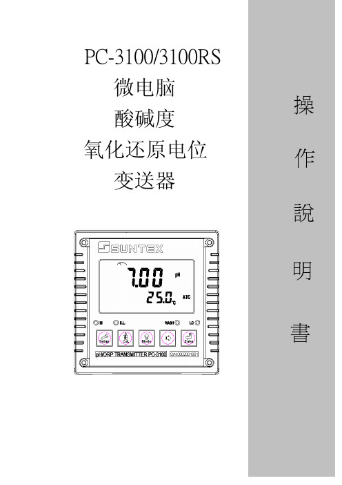
一、 规格
机型 测试项目 测 试 范 围 解 析 度 精 确 度 pH ORP TEMP pH ORP TEMP pH ORP TEMP PC-3100 pH/ORP/TEMP -2.00~16.00pH -1999~1999mV -30.0~130.0C 0.01pH 1mV 0.1C ±0.01± 1 Digit ±0.1% ± 1 Digit ±0.2C± 1 Digit 具温度误差修正功能 NTC30K/ PT1000 自动温度补偿 手动温度补偿 自定义单双点校正及预设 Tech & 自定义单双点校正及预设 Tech、 NIST 标准液两点自动校正 NIST 标准液两点或三点自动校正 0~50C -20~70C > 1012 Ω 背光式大型液晶显示,具背光感应器做自动及手动背光选择 隔离式 0/4~20mA 可设定对应 pH/ORP 量测范围,最大负载 500 隔离式 0/4~20mA 可设定对应温度 量测范围,最大负载 500 - HI/LO 两组独立之控制点 接点输出,ON 0~9999 秒 / OFF 0~999.9 小时 DC±12V IP65 100V~240VAC±10%,50/60Hz 壁挂式/管路式/盘面式 144 mm 144 mm 115 mm (HWD) 138 mm 138 mm (HW) 0.8Kg
Sensorex CX3100智能高温导电度传感器产品规格表说明书

CX3100 INTELLIGENT (HIGH TEMP)CONDUCTIVITY TRANSMITTERPRODUCT SPECIFICATION SHEET SPECIFICATIONSCalibration Mode (1) Manual cell constant adjustment(2) Conductivity standard solution calibrationCell Constants0.1 cm-1 or 10 cm-1 fixedor Freely selectable 0.0080-19.99 cm-1Analog Output 1Isolated DC 0/4-20mA (Measurement),Max load 500 ΩAnalog Output 2Isolated DC 0/4-20mA (Temperature),Max load 500 ΩAmbient Temperature0°C to 50°CStorage Temperature -20°C to 70°CTemperature Compensation Automatic: PT1000 or PT100or ManualTemperature Coefficient Linear compensation 0.00-40.00%Non-linear compensation for pure water Power Requirement100-240V AC ±10%, 7W Max, 50/60 Hz Mounting Options Panel or Wall MountDimensions½ DIN: 144mm (5.7in) x 144mm (5.7in) x115mm (4.5in)Weight0.8 kg (1.8 lbs)Enclosure IP65 (NEMA 4X)Display LCM, auto-sense backlight, contrast,text mode The CX3100 replaces the Sensorex CX3000 as our conductivity, resistivity, TDS, and salinity monitoring instrument in a ½ DIN size.This transmitter / controller is ideal for boiler applications, providing accurate temperature compensated readings up to 200°C (the highest of any of our instruments). With PT1000 temperature compensation, the CX3100 is compatible with Sensorex’s best in class stainless steel boiler conductivity probes (CS675, CS676, and CS875). The CX3100 features brand new firmware and an updated user interface with user friendly text and graphical illustrations. This makes the instrument more intuitive to use compared with the older CX3000. Monitor Conductivity, TDS, Resistivity or Salinity Programmable Hi/Hi, Hi/Lo, Lo/Lo Relays2 analog 4-20mA outputsAutomatic temperature compensation up to 200°C User friendly text and graphical illustrationsConductivityRange: 0.000 uS/cm - 2000 mS/cmin 7 ranges (auto or fixed)Resolution:0.001 / 0.01 / 0.1 / 1 uS/cm(0.01 / 0.1 / 1 mS/cm)Accuracy: ±1%ResistivityRange: 0.00-20.0 MΩ-cmResolution: 0.01 MΩ-cmAccuracy: ±1%TDS Range: 0 ppm-19,999 ppm(0.00 ppt-199.99 ppt)Salinity Range: 0.0 ppt-70.0 ppt TemperatureRange: -30°C to 200°CResolution: 0.1°CAccuracy: ±0.2°CMEASUREMENTS DESIGNED AND ASSEMBLED IN CALIFORNIA, USA。
Fairchild Semiconductor FAN3100单通道2A高速低端门极驱动器说明书

Features 特征 ▪ V DD = 12V 时峰值灌电流/源电流可达3A ▪ 4.5-18V 工作电压范围▪ V OUT = 6V 时2.5A 灌电流/1.8A 源电流▪ 双逻辑输入均可通过使能功能配置成非反相或反相逻辑▪ 无输入时内置电阻可关断驱动器▪ 1nF 负载时典型上升时间13ns 和典型下降时间9ns ▪ 可选TTL 或 CMOS 输入阈值 ▪ MillerDrive™技术▪ 输入下降沿或上升沿时典型的传输延时时间均低于20ns▪ 6-引线 2x2mm MLP 或 5-管脚SOT23封装 ▪额定环境温度范围-40°C - +125°C应用场合 ▪ 开关电源▪ 高效MOSFET 开关 ▪ 同步整流电路 ▪ DC-DC 变换器 ▪电动机控制说明FAN3100为2A 门极驱动器,在较短的开关间隔内,能够提供较高的峰值电流脉冲,设计用于驱动低端开关应用领域的N-沟道增强型MOSFET 。
该驱动器能够兼容TTL (FAN3100T) 或 CMOS (FAN3100C)输入阈值。
其内部电路设计有欠压闭锁功能,欠压时能够保持输出低电平,直到电源电压恢复到正常工作范围为止。
FAN3100能够满足快速MOSFET 开关性能,在高频电力变换器设计中,有利于最大限度地提升效率。
FAN3100驱动器的输出级集成有MillerDrive™结构。
在MOSFET 开通与关断过程的米勒平台阶段,这种双极-MOSFET 组合能够提供较高的峰值电流,使得开关损耗大大降低,同时提供有轨-轨电压摆幅和反向电流能力。
FAN3100还支持双输入,均可通过使能功能配置成非反相或反相模式。
如果任一通道或双通道没有接线,内部电阻能够为输入提供偏置,拉低输出,保持功率MOSFET 关断。
FAN3100封装可选用尺寸最小、热性能最优的2x2mm 6-引线制模无铅封装 (MLP) 或符合工业标准的5-管脚SOT23封装。
宏杉存储MS3000、MS5000维护手册
宏杉存储MS3000、MS5000维护手册MacroSAN MS5000 MS3000系列产品维护手册文档版本:V1.11 硬件状态检查1.1 产品外观○i说明MS5000/MS3000/MS2500系列存储设备的外观相似,在下面的描述中以MS5000系列存储设备的外观为例进行说明。
1.1.1 SPU外观1. S PU前正视图SPU的高度为4U,前正视图如图1-1所示。
图1-1SPU前正视图表1-1SPU前正视图组件说明组件描述(1)前面板SPU的前面板,取下前面板后是2个电池模块插槽,可插入电池模块(2)磁盘模块插槽1-16 SPU前端提供16个3.5英寸磁盘模块插槽,可插入3.5英寸磁盘模块(兼容3.5英寸磁盘和2.5英寸磁盘)2. S PU后正视图○i说明SPU可插入2个SP、2个电源模块、2个风扇模块,为方便布线以及提供更好的散热效果,插入SPU下部的模块正立放置,模块编号为1,比如SP1;插入SPU上部的模块倒立放置,模块编号为2,比如SP2。
SP中可插入不同类型的IO插卡(包括FC 插卡、GE插卡、10GE插卡等),SPU 后正视图和SP正视图以插入FC插卡为例进行说明。
MS2500系列存储设备标配一种IO插卡,不能选配,详细规格请参见错误!未找到引用源。
节。
△!注意要求插入同一个SPU的两个SP的型号相同,否则设备无法正常启动。
SPU的后端提供了SP插槽、电源模块插槽、风扇模块插槽,各个模块均支持热插拔。
SPU后正视图如图1-2所示。
图1-2SPU后正视图表1-2SPU后正视图组件说明组件描述(1)防静电手腕插孔用于连接防静电手腕,以防止人体静电损坏敏感元器件(2)SP2 SPU的SP插槽2,可插入SP(3)FAN2 SPU的风扇模块插槽2,可插入风扇模块(4)PS1 SPU的电源模块插槽1,可插入电源模块(5)接地端子用于接地,以防止设备的漏电流对人体产生电击(6)SP1 SPU的SP插槽1,可插入SP(7)FAN1 SPU的风扇模块插槽1,可插入风扇模块(8)PS2 SPU的电源模块插槽2,可插入电源模块3. S P正视图△!注意对于MS5000/MS3000系列存储设备,要求插入两个SP的IO插卡型号必须相同,且相同型号的IO插卡必须插入两个SP中相同的插槽。
XL3005规格书(中文版)

打印名称 XL3005E1
封装方式 TO263-5L
包装类型 800 只每卷
XLSEMI 无铅产品,产品型号带有“E1”后缀的符合 RoHS 标准。
绝对最大额定值(注 1)
参数 输入电压 输出开关引脚电压 电流采样引脚电压 功耗 热阻 (TO263-5L) (结到环境,无外部散热片) 最大结温 操作结温 贮存温度范围 引脚温度(焊接10秒) ESD (人体模型)
85.0
82.5
VIN=8V,IOUT=1540mA
80.0 77.5
VIN=12V,IOUT=1540mA VIN=24V,IOUT=1540mA VIN=36V,IOUT=1540mA
75.0
72.5
70.0
67.5
65.0
62.5
60.0
1
2
3
4
5
6
7
8
9
10
LED String(N*5W)
图20. XL3005系统效率曲线
220KHz 36V 5A开关电流降压型LED恒流驱动器
Datasheet
XL3005
特点
n 8V到36V宽输入电压范围 n 0.21V输出电流采样电压 n 最大占空比100% n 最小压差0.3V n 固定220KHz开关频率 n 最大5A开关电流 n 内置功率MOS n 出色的线性与负载调整率 n 内置频率补偿功能 n 内置输出短路保护功能 n 内置热关断功能 n 内置电流限制功能 n TO263-5L封装
Recommend output voltage safe work range
30
28
26
IOUT=2000mA
LM3100资料

LM3100SIMPLE SWITCHER ®Synchronous 1MHz 1.5A Step-Down Voltage RegulatorGeneral DescriptionThe LM3100Synchronously Rectified Buck Converter fea-tures all functions needed to implement a highly efficient,cost effective buck regulator capable of supplying 1.5A to loads with voltages as low as 0.8V.Dual 40V N-Channel synchronous MOSFET switches allow for low external com-ponent thus reducing complexity and minimizing board space.The LM3100is designed to work exceptionally well with ceramic and other very low ESR output capacitors.The Constant ON-Time (COT)regulation scheme requires no loop compensation,results in fast load transient response,and simplifies circuit implementation.Through the use of a unique design the regulator does not rely on output capacitor ESR for stability,as do most other COT regulators.The operating frequency remains nearly constant with line and load variations due to the inverse relationship between the input voltage and the on-time.The oprating frequency can be externally programmed up to 1MHz.Protection features include V CC under-voltage lockout,thermal shutdown and gate drive under-voltage lockout.The part is available in a thermally enhanced eTSSOP-20packageFeaturesn Input voltage range 4.5V -36V n 1.5A output current n 0.8V,±1.5%referencen Integrated 40V,dual N-Channel buck synchronous switchesn Low component count and small solution size n No loop compensation required n Ultra-fast transient responsen Stable with ceramic and other low ESR capacitors n Programmable switching frequency up to 1MHz n Max.duty cycle limited during start-up n Valley current limitn Precision Internal Reference for adjustable output voltage down to 0.8V n Thermal shutdownnThermally enhanced eTSSOP-20packageTypical Applicationsn 5VDC,12VDC,24VDC,12VAC,and 24VAC systems n Embedded Systems n Industrial Controlsn Automotive Telematics and Body Electronics n Point of Load Regulators n Storage Systemsn Broadband InfrastructurenDirect Conversion from 2/3/4Cell Lithium Batteries SystemsTypical Application20174702SIMPLE SWITCHER ®is a registered trademark of National Semiconductor CorporationFebruary 2006LM3100SIMPLE SWITCHER ®Synchronous 1MHz 1.5A Step-Down Voltage Regulator©2006National Semiconductor Corporation Connection Diagram2017470320-lead Plastic eTSSOP (MXA20A)Ordering InformationOrder Number Package Type NSC Package DrawingSupplied AsLM3100MH Exposed Pad TSSOP-20MXA002073units per Anti-Static Tube LM3100MHX2500Units on Tape and ReelL M 3100 2LM3100 Pin DescriptionsPin Name Description Application Information1,9,10,12,19,20N/C No Connection These pins must be left unconnected.2,3SW Switching Node Internally connected to the buck switch source.Connect to output inductor.4,5VIN Input supply voltage Supply pin to the device.Nominal input range is4.5V to36V.6BST Connection for bootstrap capacitor Connect a0.033µF capacitor from SW pin to thispin.An internal diode charges the capacitor duringthe high-side switch off-time.7GND Analog Ground Ground for all internal circuitry other than thesynchronous switches.8SS Soft-start An internal8µA current source charges an externalcapacitor to provide the soft-start function.11TST Test mode enable pin Force the device into test mode.Must be connectedto ground for normal operation.13FB Feedback Internally connected to the regulation andover-voltage comparators.The regulation setting is0.8V at this pin.Connect to feedback divider.14EN Enable pin Connect a voltage higher than1.26V to enable theregulator.15RON On-time Control An external resistor from VIN to this pin sets thehigh-side switch on-time.16VCC Start-up regulator Output Nominally regulated to6V.Connect a capacitor ofnot less than680nF between VCC and GND forstable operation.17,18PGND Power Ground Synchronous rectifier MOSFET source connection.Tie to power ground plane.DAP EP Exposed Pad Thermal connection pad,connect to GND.3Absolute Maximum Ratings (Note 1)If Military/Aerospace specified devices are required,please contact the National Semiconductor Sales Office/Distributors for availability and specifications.VIN,RON to GND -0.3V to 40V SW to GND-0.3V to 40V SW to GND (Transient)-2V (<100ns)VIN to SW -0.3V to 40V BST to SW-0.3V to 7V All Other Inputs to GND-0.3V to 7VESD Rating (Note 2)Human Body Model ±2kVStorage Temperature Range -65˚C to +150˚CJunction Temperature (T J )150˚COperating Ratings (Note 1)Supply Voltage Range (VIN) 4.5V to 36V Junction Temperature Range (T J )−40˚C to +125˚CThermal Resistance (θJC )(Note 3)6.5˚C/WElectrical CharateristicsSpecifications with standard type are for T J =25˚C only;limits in boldface type ap-ply over the full Operating Junction Temperature (T J )range.Minimum and Maximum limits are guaranteed through test,de-sign,or statistical correlation.Typical values represent the most likely parametric norm at T J =25˚C,and are provided for ref-erence purposes only.Unless otherwise stated the following conditions apply:V IN =18V,V OUT =3.3V.SymbolParameterConditionsMinTypMaxUnitsStart-Up Regulator,V CCV CC V CC output voltage C CC =680nF,no load 5.06.07.2V V IN -V CC V IN -V CC dropout voltage I CC =2mA 50140mVI CC =20mA 350570I VCCL V CC current limit (Note 4)V CC =0V 4065mA V CC-UVLO V CC under-voltage lockout threshold (UVLO)V IN increasing 3.6 3.75 3.85V V CC-UVLO-HYS V CC UVLO hysteresis V IN decreasing130mV t VCC-UVLO-DV CC UVLO filter delay 3µs I IN I IN operating currentNo switching,V FB =1V0.71mA I IN-SD I IN operating current,Device shutdown V EN =0V 1730µA Switching CharacteristicsR DS-UP-ON Main MOSFET Rds(on)0.180.35ΩR DS-DN-ON Syn.MOSFET Rds(on)0.110.2ΩV G-UVLOGate drive voltage UVLOV BST -V SW increasing 3.34V Soft-startI SSSS pin source currentV SS =0.5V689.8µACurrent LimitI CLSyn.MOSFET current limit threshold1.9AON/OFF Timert ON ON timer pulse widthV IN =10V,R ON =100k Ω 1.38µsV IN =30V,R ON =100k Ω0.47t ON-MIN ON timer minimum pulse width 200ns t OFFOFF timer pulse width260ns Enable InputV EN EN Pin input threshold V EN rising 1.2361.26 1.285V V EN-HYSEnable threshold hysteresis V EN falling90mV Regulation and Over-Voltage ComparatorV FBIn-regulation feedback voltageV SS ≥0.8VT J =−40˚C to +125˚C 0.7840.80.816VV SS ≥0.8VT J =0˚C to +125˚C0.7880.812V FB-OV Feedback over-voltage threshold0.8940.9200.940V I FB5100nAThermal ShutdownT SDThermal shutdown temperatureT J rising165˚CL M 3100 4LM3100Electrical Charateristics Specifications with standard type are for T=25˚C only;limits in boldface type applyJover the full Operating Junction Temperature(T J)range.Minimum and Maximum limits are guaranteed through test,design,or statistical correlation.Typical values represent the most likely parametric norm at T J=25˚C,and are provided for referencepurposes only.Unless otherwise stated the following conditions apply:V IN=18V,V OUT=3.3V.(Continued) Symbol Parameter Conditions Min Typ Max Units T SD-HYS Thermal shutdown temperatureT J falling20˚C hysteresisNote1:Absolute Maximum Ratings are limits beyond which damage to the device may occur.Operating Ratings are conditions under which operation of the deviceis intended to be functional.For guaranteed specifications and test conditions,see the Electrical Characteristics.Note2:The human body model is a100pF capacitor discharged through a1.5kΩresistor into each pin.Note3:θJC measurements are performed in general accordance with Mil-Std883B,Method1012.1and utilizes the copper heat sink technique.Copper Heat Sink@60˚C.Note4:V CC provides self bias for the internal gate drive and control circuits.Device thermal limitations limit external loading.5Typical Performance CharacteristicsAll curves taken at V IN =18V with configuration in typical ap-plication circuit for V OUT=3.3V shown in this datasheet.T A =25˚C,unless otherwise specified.Quiescent Current,I IN vs V INV CC vs I CC2017471820174719V CC vs V IN T ON vs V IN2017472020174721Switching Frequency,F SW vs V IN V FB vs Temperature2017472220174723L M 3100 6Typical Performance Characteristics All curves taken at V IN =18V with configuration in typicalapplication circuit for V OUT =3.3V shown in this datasheet.T A =25˚C,unless otherwise specified.(Continued)R DS(ON)vs TemperatureEfficiency vs Load Current(V OUT =3.3V)2017472420174725V OUT Regulation vs Load Current(V OUT =3.3V)Efficiency vs Load Current(V OUT =0.8V)2017472620174727V OUT Regulation vs Load Current(V OUT =0.8V)Power Up(V OUT=3.3V,1.5A Loaded)2017472820174729LM31007Typical Performance Characteristics All curves taken at V IN =18V with configuration in typicalapplication circuit for V OUT =3.3V shown in this datasheet.T A =25˚C,unless otherwise specified.(Continued)Enable Transient(V OUT =3.3V,1.5A Loaded)Shutdown Transient (V OUT =3.3V,1.5A Loaded)2017473020174731Continuous Mode Operation (V OUT =3.3V,1.5A Loaded)Discontinuous Mode Operation (V OUT =3.3V,1.5A Loaded)2017473220174733CCM to DCM Transition(V OUT =3.3V,0.15A -1.5A Load)Load Transient(V OUT=3.3V,0.15A -1.5A Load,Current slew-rate:2.5A/µs)2017473420174735L M 3100 8LM3100 Simplified Functional Block Diagram9Functional DescriptionThe LM3100Step Down Switching Regulator features all functions needed to implement a cost effective,efficient buck power converter capable of supplying 1.5A to a load.This voltage regulator contains Dual 40V N-Channel buck syn-chronous switches and is available in a thermally enhanced eTSSOP-20package.The Constant ON-Time (COT)regu-lation scheme requires no loop compensation,results in fast load transient response,and simplifies circuit implementa-tion.It will work correctly even with an all ceramic output capacitor network and does not rely on the output capacitor’s ESR for stability.The operating frequency remains constant with line and load variations due to the inverse relationship between the input voltage and the on-time.The valley cur-rent limit detection circuit,internally set at 1.9A,inhibits the high-side switch until the inductor current level subsides.Please refer to the functional block diagram with a typical application circuit.The LM3100can be applied in numerous applications and can operate efficiently from inputs as high as 36V.Protection features include:Thermal shutdown,V CC under-voltage lockout,gate drive under-voltage lockout.Hysteretic Control Circuit OverviewThe LM3100buck DC-DC regulator employs a control scheme in which the high-side switch on-time varies in-versely with the line voltage (V IN ).Control is based on a comparator and the one-shot on-timer,with the output volt-age feedback (FB)compared with an internal reference of 0.8V.If the FB level is below the reference the buck switch is turned on for a fixed time determined by the input voltage and a programming resistor (R ON ).Following the on-time,the switch remains off for a minimum of 260ns.If FB is below the reference at that time the switch turns on again for another on-time period.The switching will continue until regulation is achieved.The regulator will operate in discontinuous conduction mode at light load currents,and continuous conduction mode with heavy load current.In discontinuous conduction mode (DCM),current through the output inductor starts at zero and ramps up to a peak during the on-time,then ramps back to zero before the end of the off-time.The next on-time period starts when the voltage at FB falls below the internal refer-ence.Until then the inductor current remains zero and the load is supplied entirely by the output capacitor.In this mode the operating frequency is lower than in continuous conduc-tion mode,and varies with load current.Conversion effi-ciency is maintained since the switching losses are reduced with the reduction in load and switching frequency.The discontinuous operating frequency can be calculated ap-proximately as follows:(1)where R L =the load resistanceIn continuous conduction mode (CCM),current always flows through the inductor and never reaches zero during the off-time.In this mode,the operating frequency remains rela-tively constant with load and line variations.The CCM oper-ating frequency can be calculated approximately as follows:(2)The output voltage is set by two external resistors (R FB1,R FB2).The regulated output voltage is calculated as follows:V OUT =0.8V x (R FB1+R FB2)/R FB2(3)Start-up Regulator (V CC )The start-up regulator is integrated within LM3100.The input pin (VIN)can be connected directly to line voltage up to 36V,with transient capability to 40V.The V CC output regulates at 6V,and is current limited to 65mA.Upon power up,the regulator sources current into the external capacitor at V CC (C VCC ).C VCC must be at least 680nF for stability.When the voltage on the VCC pin reaches the under-voltage lockout threshold of 3.75V,the buck switch is enabled and the Soft-start pin is released to allow the soft-start capacitor (C SS )to charge.The minimum input voltage is determined by the dropout voltage of V CC ,and the V CC UVLO falling threshold ()3.7V).If VIN is less than )4.0V,the V CC UVLO activates to shut off the output.Regulation ComparatorThe feedback voltage at FB is compared to the internal reference voltage of 0.8V.In normal operation (the output voltage is regulated),an on-time period is initiated when the voltage at FB falls below 0.8V.The buck switch stays on for the on-time,causing the FB voltage to rise above 0.8V.After the on-time period,the buck switch stays off until the FB voltage falls below 0.8V.Bias current at the FB pin is nomi-nally 100nA.Over-Voltage ComparatorThe voltage at FB is compared to an internal 0.92V refer-ence.If the voltage at FB rises above 0.92V the on-time pulse is immediately terminated.This condition can occur if the input voltage,or the output load,changes suddenly.Once the OVP is activated,the buck switch remains off until the voltage at FB pin falls below 0.92V.The low side switch will stay on to discharge the inductor energy and until the inductor current decays to zero.The low side switch will be turned off.ON-Time Timer,ShutdownThe LM3100main switch is determined by the R ON resistor and the input voltage (V IN ),and is calculated from:(4)The inverse relationship with VIN results in a nearly constant frequency as V IN is varied.R ON should be selected for a minimum on-time (at maximum V IN )greater than 200ns for proper current limit operation.This requirement limits the maximum frequency for each application,depending on V IN and V OUT ,calculated from the following:L M 3100 10ON-Time Timer,Shutdown(Continued)(5)The LM3100can be remotely shut down by taking the EN pin below 1.1V.Refer to Figure 1.In this mode the SS pin is internally grounded,the on-timer is disabled,and bias cur-rents are reduced.Releasing the EN pin allows normal operation to resume.The voltage at the EN pin is between 1.5V and 3.0V,depending on V IN and the pull-up resistor.Current LimitCurrent limit detection occurs during the off-time by monitor-ing the re-circulating current through the low-side synchro-nous switch.Referring to Functional Block Diagram,when the buck switch is turned off,inductor current flows through the load,into PGND,and through the internal low-side syn-chronous switch.If that current exceeds 1.9A the current limit comparator toggles,forcing a delay to the start of the next on-time period.The next cycle starts when the re-circulating current falls back below 1.9A and the voltage at FB is below 0.8V.The inductor current is monitored during the low-side switch on-time.As long as the overload condi-tion persists and the inductor current exceeds 1.9A,the high-side switch will remain inhibited.The operating fre-quency is lower during an over-current due to longer than normal off-times.Figure 2illustrates the inductor current waveform.During normal operation the load current is low,the average of the ripple waveform.When an overload occurs the current ratch-ets up until it exceeds 1.9A.During the Current Limited portion of Figure 2,the current ramps down to 1.9A during each off-time,initiating the next on-time (assuming the volt-age at FB is <0.8V).During each on-time the current ramps up an amount equal to:(6)During this time the LM3100is in a constant current mode,with an average load current (I OCL )equal to 1.9A +∆I/2.20174704FIGURE 1.Shutdown Implementation20174705FIGURE 2.Inductor Current -Current Limit OperationLM310011N -Channel Buck Switch and DriverThe LM3100integrates an N-Channel buck (high-side)switch and associated floating high voltage gate driver.The gate drive circuit works in conjunction with an external boot-strap capacitor and an internal high voltage diode.A 33nF capacitor (C BST )connected between BST and SW pins pro-vides voltage to the high-side driver during the buck switch on-time.During each off-time,the SW pin falls to approxi-mately -1V and C BST charges from the V CC supply through the internal diode.The minimum off-time of 260ns ensures adequate time each cycle to recharge the bootstrap capaci-tor.SoftstartThe soft-start feature allows the converter to gradually reach a steady state operating point,thereby reducing start-up stresses and current surges.Upon turn-on,after V CC reaches the under-voltage threshold,an internal 8µA current source charges up the external capacitor at the SS pin.The ramping voltage at SS (and the non-inverting input of the regulation comparator)ramps up the output voltage in a controlled manner.An internal switch grounds the SS pin if V CC is below the under-voltage lockout threshold,if a thermal shutdown oc-curs,or if the EN pin is ing an externally controlled switch,the output voltage can be shut off by taking the SS pin to ground.Releasing the switch allows the SS pin to ramp up,and the output voltage to return to normal.The shut-down configuration is shown in Figure 3.Thermal ProtectionThe LM3100should be operated so the junction temperature does not exceed the maximum limit.An internal Thermal Shutdown circuit,which activates (typically)at 165˚C,takes the controller to a low power reset state by disabling the buck switch and the on-timer,and grounding the Softstart pin.This feature helps prevent catastrophic failures from accidental device overheating.When the junction temperature falls back below 145˚C (typical hysteresis =20˚C),the Softstart pin is released and normal operation resumes.Applications InformationEXTERNAL COMPONENTSThe following guidelines can be used to select the external components.R FB1and R FB2:The ratio of these resistors is calculated from:R FB1/R FB2=(V OUT /0.8V)-1R FB1and R FB2should be chosen from standard value resis-tors in the range of 1.0k Ω-10k Ωwhich satisfy the above ratio.For V OUT =0.8V,the FB pin can be connected to the output directly.However,the converter operation needs a minimum inductor current ripple to maintain good regulation when no load is connected.This minimum load is about 10µA and can be implemented by adding a pre-load resistor to the output.R ON :The minimum value for RON is calculated from:Equation 1can be used to select R ON if a specific frequency is desired as long as the above limitation is met.L:The main parameter effected by the inductor is the output current ripple amplitude (I OR ).The maximum allowable (I OR must be determined at both the minimum and maximum nominal load currents.At minimum load current,the lower peak must not reach 0mA.At maximum load current,the upper peak must not exceed the current limit threshold (1.9A).The allowable ripple current is calculated from the following equations:I OR(MAX1)=2x I O(min)orI OR(MAX2)=2x (1.9A -I O(max))The lesser of the two ripple amplitudes calculated above is then used in the following equation:(7)where V IN is the maximum input voltage and Fs is deter-mined from equation 1.This provides a value for L.The next larger standard value should be used.L should be rated for the I PK current level shown in Figure 2.Inductor Selector for V OUT =3.3V2017473620174706FIGURE 3.Alternate Shutdown ImplementationL M 3100 12Applications Information(Continued)Inductor Selector for V OUT=0.8V20174737C VCC:The capacitor on the V CC output provides not onlynoise filtering and stability,but also prevents false triggeringof the V CC UVLO at the buck switch on/off transitions.Forthis reason,C VCC should be no smaller than680nF forstability,and should be a good quality,low ESR,ceramiccapacitor.C O and C O3:C O should generally be no smaller than10µF.Experimentation is usually necessary to determine the mini-mum value for C O,as the nature of the load may require alarger value.A load which creates significant transients re-quires a larger value for C O than a fixed load.C O3is a small value ceramic capacitor to further suppresshigh frequency noise at V OUT.A47nF is recommended,located close to the LM3100.C IN and C IN3:C IN’s purpose is to supply most of the switchcurrent during the on-time,and limit the voltage ripple at V IN,on the assumption that the voltage source feeding V IN hasan output impedance greater than zero.If the source’s dy-namic impedance is high(effectively a current source),itsupplies the average input current,but not the ripple current.At maximum load current,when the buck switch turns on,thecurrent into V IN suddenly increases to the lower peak of theinductor’s ripple current,ramps up to the peak value,thendrop to zero at turn-off.The average current during theon-time is the load current.For a worst case calculation,C INmust supply this average load current during the maximumon-time.C IN is calculated from:(8)where I O is the load current,t ON is the maximum on-time,and∆V is the allowable ripple voltage at V IN.C IN3’s purpose is to help avoid transients and ringing due tolong lead inductance at V IN.A low ESR,0.1µF ceramic chipcapacitor is recommended,located close to the LM3100.C BST:The recommended value for CBST is33nF.A highquality ceramic capacitor with low ESR is recommended asC BST supplies a surge current to charge the buck switch gateat turn-on.A low ESR also helps ensure a complete rechargeduring each off-time.C SS:The capacitor at the SS pin determines the soft-starttime,i.e.the time for the reference voltage at the regulationcomparator,and the output voltage,to reach their final value.The time is determined from the following:C FB:If output voltage is higher than1.6V,this feedback capis needed for Discontinuous Conduction Mode to improvethe output ripple performance,the recommended value forC FB is10nF.PC BOARD LAYOUTThe LM3100regulation,over-voltage,and current limit com-parators are very fast,and will respond to short durationnoise yout considerations are therefore critical foroptimum performance.The layout must be as neat andcompact as possible,and all of the components must be asclose as possible to their associated pins.Refer to thefunctional block diagram,the loop formed by C IN,the highand low-side switches internal to the IC,and the PGND pinshould be as small as possible.The PGND connection to Cinshould be as short and direct as possible.There should beseveral vias connecting the Cin ground terminal to theground plane placed as close to the capacitor as possible.The boost capacitor should be connected as close to the SWand BST pins as possible.The feedback divider resistorsand the C FB capacitor should be located close to the FB pin.A long trace run from the top of the divider to the output isgenerally acceptable since this is a low impedance node.Ground the bottom of the divider directly to the GND(pin7).The output capacitor,C OUT,should be connected close tothe load and tied directly into the ground plane.The inductorshould connect close to the SW pin with as short a trace aspossible to help reduce the potential for EMI(electro-magnetic interference)generation.If it is expected that the internal dissipation of the LM3100will produce excessive junction temperatures during normaloperation,good use of the PC board’s ground plane can helpconsiderably to dissipate heat.The exposed pad on thebottom of the IC package can be soldered to a ground planeand that plane should extend out from beneath the IC to helpdissipate the heat.The exposed pad is internally connectedto the IC substrate.Additionally the use of wide PC boardtraces,where possible,can help conduct heat away from theing numerous vias to connect the die attach pad to aninternal ground plane is a good practice.Judicious position-ing of the PC board within the end product,along with theuse of any available air flow(forced or natural convection)can help reduce the junction temperature.LM310013Applications Information(Continued)20174716Typical Application Schematic for V OUT =3.3V20174717Typical Application Schematic for V OUT =0.8VL M 3100 14Physical Dimensionsinches (millimeters)unless otherwise noted20-Lead Plastic eTSSOP Package NS Package Number MXA20ANational does not assume any responsibility for use of any circuitry described,no circuit patent licenses are implied and National reserves the right at any time without notice to change said circuitry and specifications.For the most current product information visit us at .LIFE SUPPORT POLICYNATIONAL’S PRODUCTS ARE NOT AUTHORIZED FOR USE AS CRITICAL COMPONENTS IN LIFE SUPPORT DEVICES OR SYSTEMS WITHOUT THE EXPRESS WRITTEN APPROVAL OF THE PRESIDENT AND GENERAL COUNSEL OF NATIONAL SEMICONDUCTOR CORPORATION.As used herein:1.Life support devices or systems are devices or systems which,(a)are intended for surgical implant into the body,or (b)support or sustain life,and whose failure to perform when properly used in accordance with instructions for use provided in the labeling,can be reasonably expected to result in a significant injury to the user.2.A critical component is any component of a life support device or system whose failure to perform can be reasonably expected to cause the failure of the life support device or system,or to affect its safety or effectiveness.BANNED SUBSTANCE COMPLIANCENational Semiconductor follows the provisions of the Product Stewardship Guide for Customers (CSP-9-111C2)and Banned Substances and Materials of Interest Specification (CSP-9-111S2)for regulatory environmental compliance.Details may be found at:/quality/green.Lead free products are RoHS compliant.National Semiconductor Americas Customer Support CenterEmail:new.feedback@ Tel:1-800-272-9959National SemiconductorEurope Customer Support CenterFax:+49(0)180-5308586Email:europe.support@Deutsch Tel:+49(0)6995086208English Tel:+44(0)8702402171Français Tel:+33(0)141918790National Semiconductor Asia Pacific Customer Support CenterEmail:ap.support@National SemiconductorJapan Customer Support Center Fax:81-3-5639-7507Email:jpn.feedback@ Tel:81-3-5639-7560LM3100SIMPLE SWITCHER ®Synchronous 1MHz 1.5A Step-Down Voltage Regulator。
6639S-1-103;6639S-1-102;6639S-1-104;6639S-1-202;6639S-1-203;中文规格书,Datasheet资料
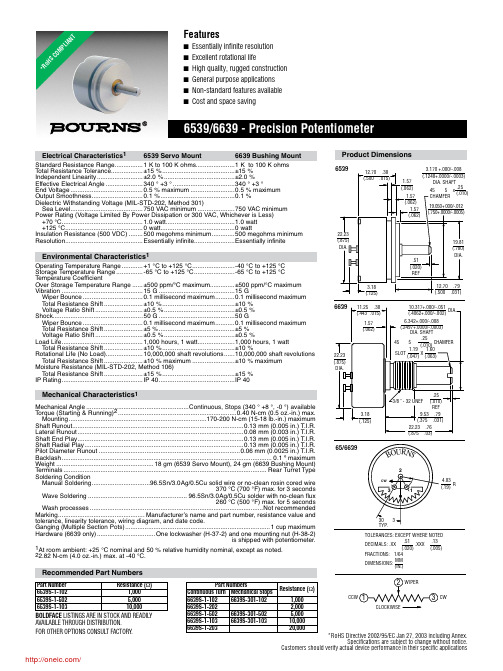
22.23 (.875) DIA.
3.18 (.125)
6639
11.25 .38 (.443 .015)
1.57 (.062)
Байду номын сангаас
22.23 (.875) DIA.
.51 (.020) REF
19.81 (.780) DIA.
12.70 .79 (.500 .031)
10.317+.000/-.051 (.4062+.000/-.002)
DIA.
6.342+.000/-.008
(.2497+.0000/-.0003) DIA. SHAFT .25
45 5 (.010) CHAMFER 1.19 1.60
SLOT (.047) X (.063)
Mechanical Characteristics1
Mechanical Angle ..........................................................Continuous, Stops (340 ° +8 °, -0 °) available Torque (Starting & Running)2 ...................................................................0.40 N-cm (0.5 oz.-in.) max.
Sea Level......................................... 750 VAC minimum .....................750 VAC minimum Power Rating (Voltage Limited By Power Dissipation or 300 VAC, Whichever is Less)
Power Xpert Meter 350 (PXM350) 技术数据TD150024EN说明书

ContentsDescription Page Product overview . . . . . . . . . . . . . . . . . . . . . . . . . .2Key features . . . . . . . . . . . . . . . . . . . . . . . . . . . . . .2Wide voltage range . . . . . . . . . . . . . . . . . . . . . . . .2Ordering information . . . . . . . . . . . . . . . . . . . . . . .2Additional features . . . . . . . . . . . . . . . . . . . . . . . . .2PXM350 functions comparison . . . . . . . . . . . . . . .3Metering . . . . . . . . . . . . . . . . . . . . . . . . . . . . . . . .4Specifications . . . . . . . . . . . . . . . . . . . . . . . . . . . .4Typical wiring for 5 A/1 A current input . . . . . . . . .5Typical wiring for RCT/mV/mA current input . . . . .6Power Xpert Meter 350 (PXM350)three-phased DIN-rail multifunction meterFeatures• Revenue grade accuracy: ANSI C12 .20 0 .5 Class • Measurement Canada approved• Tamper-proof sealing design approved for revenue applications • Wide voltage measurement range, directly measure up to 690 V • Multiple current sensor input options compatible with any CT • Built-in Modbus RTU, BACnet MSTP , and pulse output • Auto-wiring check to verify correct installation •SunSpec support2Technical Data TD150024ENEffective August 2019Power Xpert Meter 350 (PXM350)three-phased DIN-rail multifunction meterEATON Product overviewThe PXM350 DIN rail meter combines high performance with ease of integration to provide a cost-effective power and energy monitoring solution . Featuring a built-in liquid crystal display (LCD) designed to simplify setup and local reading of meter data . While the Modbus-RTU, BACnet MSTP , and pulse output communication allows seamless integration with data acquisition systems .Key featuresThe PXM350 series of three-phase multi-circuit power and energy meters offer revenue grade accuracy and a wealth of other features, including:•Utility Revenue Grade Accuracy - IEC 62053-22 0 .5s Class / ANSI C12 .20 0 .5 Class;•Multiple CT input options compatible with any CT : 5 A/1 A, 333 mV , flexible Rogowski coil, 80/100/200 mA;• Four-channel current input including neutral current measurement;• Residual current measurement available;•10-690 Vac direct voltage input, one model for most low voltage circuits;•RS-485 port built-in with Modbus-RTU or BACnet MSTP provides standard integration with most systems;• Standard Din-rail mount for ease-of-installation;• Compatible with both 50 Hz and 60 Hz systems;• Built-in energy pulse output and alarm output;• Optional relay output for alarm and remote control; and •Tamper-proof design approved for revenue applications .Wide voltage rangeVoltage: Measuring from 10 V to 400 VL -N 690 VL -L that works with most voltage ratings without a potential transformer (PT) . Potential transformer ratio configuration supported where PT is used .Frequency: Automatically adapt to 50 Hz and 60 Hz system without compromising the accuracy, which simplifies design and eliminates international frequency issues .Ordering informationPXM 350 MA 6 3 2 1Additional featuresFour channel CT inputAccurately measure neutral current with 4th CT and provide residual current measurement .Auto phase-checkDesigned to automatically check most common wiring mistakes such as CT polarity, voltage, and current phase alignment .Supports standard electrical system configurationsThree-phase three-wire (3P3W), three-phase four-wire (3P4W),single-phase three-wire (1P3W two element), single-phase two-wire (1P2W one element) and more .Current input 3 = 333 mV5 = 5 A/1 A configurable R = Rogowski coil** Bidirectional energyonly. No 4th CT input.Model type 2 = Pulse output, Modbus, BACnet MSTP , TOU4 = Pulse output, Modbus, BACnet MSTP , TOU, Bidirectional energy, 4th current inputRelay output1 = 1 relay output3Technical Data TD150024ENEffective August 2019Power Xpert Meter 350 (PXM350)three-phased DIN-rail multifunction meter EATON PXM350 functions comparisonFeaturePXM350 MA6x2xPXM350 MA6x4xBi-directional energy measurement •Active energy ••Reactive energy ••Apparent energy ••Time-of-use ••Power demand ••Peak power demand ••Predictive demand ••Current demand ••Peak current demand ••Voltage ••Current ••Neutral current Calculated•Residual current CalculatedActive power ••Reactive power ••Apparent power ••Power factor ••Frequency ••Clock ••Running time ••Energy pulse output ••Relay output (alarm or control)••RS-485 Modbus-RTU or BACnet MSTP ••Wiring check ••Temperature (internal)••SunSpec••Current transformer (CT) input 5 A/1 A: Field-configurable CT input | 333 mV: CT Input | flexible Rogowski coil CT Input | 80/100/200 mA: field-configurable CT input I/OOne relay output for alarm and remote control4Technical Data TD150024ENEffective August 2019Power Xpert Meter 350 (PXM350)three-phased DIN-rail multifunction meterEATON MeteringParameterAccuracyResolutionRangeActive energy 0.5% 1 Wh 0-999999999Reactive energy 0.5% 1 varh 0-999999999Apparent energy 0.5% 1 VAh 0-999999999Voltage 0.5%0.110 V-1000 kV Current 0.5%0.001 A 10 mA-500000 A Active power 0.5% 1 W -99-99 MW Reactive power 0.5% 1 var -99-99 Mvar Apparent power 0.5% 1 VA -99-99 MVA Power factor 0.5%0.001-0.001 to 1.000 to +0.001Frequency 0.2%0.01 Hz 50/60Power demand 0.5% 1 W/var/VA 99 MW/Mvar/MVA Current demand0.5%0.001 A10 mA-5000 ASpecificationsVoltageRated voltage 400 Vac L-N 690 Vac L-LInput impedance 2 MΩ/phase Measurement frequency 50/60 Hz Accuracy0.5%Current inputStated current (IN) 5 Aac/1 Aac Start current 10 mA Accuracy0.5%Pulse outputIsolation voltage 2500 Vac Load voltage 0~250 Vac Load current100 mA (max)Power supplyWorking power supply 100~415 Vac, 50/60 Hz,100~300 Vdc Power consumption <2 W or 10 VARelay outputLoad voltage 250 Vac 30 Vdc Max. load current 5 A (resistant load)Isolation voltage 2000 Vac (1 min.)Action time 10 ms Mechanical life20 million times Electrical lifeAbove 50,000 times (5 A, 250 Vac, resistant load)CommunicationRS-485 baud rate 1200~34800Communication protocolModbus-RTU or BACnetMSTPEnvironmentOperating temperature -25~70ºC (-13~158ºF)Storage temperature-40~85ºC (-40~185ºF)5Technical Data TD150024ENEffective August 2019Power Xpert Meter 350 (PXM350)three-phased DIN-rail multifunction meter EATON Typical wiring for 5 A/1 A current inputote:N CT shorting terminal blocks are required but not shown in the diagrams .6Technical Data TD150024ENEffective August 2019Power Xpert Meter 350 (PXM350)three-phased DIN-rail multifunction meterEATON Typical wiring for RCT/mV/mA current inputote:N CT shorting terminal blocks are required when using mA output currentsensors, but are not shown in the diagrams .7Technical Data TD150024ENEffective August 2019Power Xpert Meter 350 (PXM350)three-phased DIN-rail multifunction meter EATON Notes:Eaton1000 Eaton Boulevard Cleveland, OH 44122 United StatesEaton .com© 2019 EatonAll Rights ReservedPrinted in USAPublication No . TD150024EN/TBG001405 August 2019Eaton is a registered trademark.All other trademarks are propertyof their respective owners.Power Xpert Meter 350 (PXM350) three-phased DIN-rail multifunction meterTechnical Data TD150024ENEffective August 2019DISCLAIMER OF WARRANTIES AND LIMITATION OF LIABILITYThe information, recommendations, descriptions and safety nota-tions in this document are based on Eaton Corporation’s (“Eaton”) experience and judgment and may not cover all contingencies .If further information is required, an Eaton sales office should be consulted . Sale of the product shown in this literature is subjectto the terms and conditions outlined in appropriate Eaton selling policies or other contractual agreement between Eaton and the purchaser .THERE ARE NO UNDERSTANDINGS, AGREEMENTS, WARRANTIES, EXPRESSED OR IMPLIED, INCLUDING WARRANTIES OF FITNESS FOR A PARTICULAR PURPOSE OR MERCHANTABILITY, OTHER THAN THOSE SPECIFICALL Y SET OUT IN ANY EXISTING CONTRACT BETWEEN THE PARTIES . ANY SUCH CONTRACT STATES THE ENTIRE OBLIGATION OF EATON . THE CONTENTS OF THIS DOCUMENT SHALL NOT BECOME PART OF OR MODIFY ANY CONTRACT BETWEEN THE PARTIES .In no event will Eaton be responsible to the purchaser or user in contract, in tort (including negligence), strict liability or other-wisefor any special, indirect, incidental or consequential damage or loss whatsoever, including but not limited to damage or loss of use of equipment, plant or power system, cost of capital, loss of power, additional expenses in the use of existing power facilities, or claims against the purchaser or user by its customers resulting from the use of the information, recommendations and descriptions contained herein . The information contained in this manual is subject to change without notice .。