PMB2402中文资料
2402 酚醛树脂 平均分子量

2402 酚醛树脂平均分子量2402酚醛树脂是一种广泛应用于工业领域的合成树脂,其平均分子量约为2402。
本文将对2402酚醛树脂的特性、制备方法及应用领域进行详细介绍。
一、特性2402酚醛树脂具有以下特性:1. 耐热性好:2402酚醛树脂具有较高的耐热性,能够在高温下保持稳定性,不易熔化或分解。
2. 机械强度高:2402酚醛树脂具有良好的机械强度,具有较高的硬度和弹性模量,能够承受一定的压力和冲击。
3. 耐化学腐蚀性能好:2402酚醛树脂对大多数化学物质具有较好的耐腐蚀性,能够在酸、碱等腐蚀性环境中保持稳定性。
4. 绝缘性能优异:2402酚醛树脂具有良好的绝缘性能,能够有效隔离电流和电磁波,广泛应用于电子电气领域。
5. 成型性好:2402酚醛树脂具有较好的成型性,可通过热压、注塑等方法制备成各种形状的制品。
二、制备方法2402酚醛树脂的制备主要通过酚和甲醛的缩聚反应而得到。
具体步骤如下:1. 酚和甲醛按一定比例混合,加入催化剂促进反应。
2. 反应混合物进行缩聚反应,生成酚醛二聚体。
3. 经过后续反应,逐渐形成高聚物,最终得到2402酚醛树脂。
三、应用领域由于2402酚醛树脂具有良好的特性,因此在许多领域都有广泛的应用,主要包括以下几个方面:1. 电子电气领域:2402酚醛树脂具有良好的绝缘性能和耐热性,常用于制作电子元件、电路板、绝缘材料等。
2. 汽车工业:2402酚醛树脂具有较高的机械强度和耐热性,可用于汽车零部件的制造,如制动片、离合器片等。
3. 化工领域:由于2402酚醛树脂具有良好的耐化学腐蚀性能,常被用作储存、输送腐蚀性化学品的容器和管道材料。
4. 建筑材料:2402酚醛树脂可用于制作防火板、隔热材料和装饰材料等,具有良好的阻燃性和耐候性。
5. 其他领域:2402酚醛树脂还可用于制作模具、涂料、胶粘剂等。
总结:2402酚醛树脂是一种应用广泛的合成树脂,具有耐热性好、机械强度高、耐化学腐蚀性能好、绝缘性能优异等特性。
2402酚醛树脂产品标准 -回复

2402酚醛树脂产品标准-回复2402酚醛树脂产品标准:全面了解、应用与发展引言酚醛树脂作为一种重要的合成材料,广泛应用于家具制造、建筑材料、电子电器、汽车零部件等领域。
为了保证酚醛树脂产品的质量和安全性,2402酚醛树脂产品标准应运而生。
本文将从标准内容、应用实践以及未来发展三个方面来详细介绍2402酚醛树脂产品标准。
一、标准内容2402酚醛树脂产品标准是指对2402酚醛树脂产品的质量要求和测试方法进行规范的文件。
其标准内容主要包括以下几个方面:1. 原材料要求:对酚醛树脂的原材料要求进行详细说明,如酚醛树脂的成分、含水量、粘度等。
2. 物理性能:对酚醛树脂产品的物理性能进行测试和评估,包括强度、硬度、抗温度变形性能等。
3. 化学性能:对酚醛树脂产品的化学性能进行测试和评估,包括耐酸碱性、耐候性等。
4. 安全性:对酚醛树脂产品的有害物质浓度、挥发性有机物等进行限制和测试,以确保产品的安全性。
5. 检验方法:对酚醛树脂产品进行检验的具体方法和要求进行规定,包括取样方法、试验装置、试验步骤等。
二、应用实践2402酚醛树脂产品标准的制定为酚醛树脂行业的发展和应用提供了指导。
在实际应用中,酚醛树脂制品通常需要符合相应标准的要求,以保证产品质量和安全性。
以下是2402酚醛树脂产品标准的应用实践:1. 生产控制:生产企业需要根据产品标准制定相应的生产控制措施,确保产品的各项指标符合标准要求,提高产品的质量稳定性。
2. 质量检验:酚醛树脂制品的质量检验通常遵循产品标准的要求进行。
通过检验,可以评估产品的质量,并及时发现和解决潜在问题,提供有力的保障。
3. 市场监管:市场监管部门可以依据酚醛树脂产品标准对市场上的产品进行抽检,确保产品质量和安全性,维护市场秩序。
三、未来发展随着科学技术的不断发展和社会对环境友好型产品的需求增加,2402酚醛树脂产品标准也在不断更新和完善。
未来发展的关键点如下:1. 绿色环保:酚醛树脂产品标准应该进一步规范对有害物质的限制,提倡绿色环保的生产工艺和原材料使用,以降低对环境的影响。
SINAMICS G120 PM240P-2硬件安装手册说明书

SINAMICS SINAMICS G120 功率模块 PM240P-2
硬件安装手册
基本安全说明
1
简介
2
安装
3
接线
4
检修与维护
5
技术数据
6
备件和附件
7
附录
A
06/2020
A5E37800827B AD
Байду номын сангаас
法律资讯
警告提示系统
为了您的人身安全以及避免财产损失,必须注意本手册中的提示。人身安全的提示用一个警告三角表示,仅 与财产损失有关的提示不带警告三角。警告提示根据危险等级由高到低如下表示。
1.1
一般安全说明 ..................................................................................................................... 7
1.2
静电场或静电放电可导致设备损坏................................................................................... 13
1.3
应用示例的质保规定 ........................................................................................................ 14
1.4
安全性信息 ....................................................................................................................... 15
半导体传感器ADUM2402BRWZ中文规格书
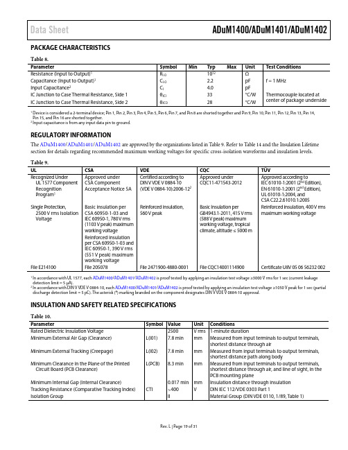
Data SheetADuM1400/ADuM1401/ADuM1402 Rev. L | Page 19 of 31PACKAGE CHARACTERISTICS Table 8.ParameterSymbol Min Typ Max Unit Test Conditions Resistance (Input to Output)1R I-O 1012 Ω Capacitance (Input to Output)1C I-O 2.2 pF f = 1 MHz Input Capacitance 2C I 4.0 pF IC Junction to Case Thermal Resistance, Side 1θJCI 33 °C/W Thermocouple located at center of package underside IC Junction to Case Thermal Resistance, Side 2θJCO 28 °C/W 1 Device is considered a 2-terminal device; Pin 1, Pin 2, Pin 3, Pin 4, Pin 5, Pin 6, Pin 7, and Pin 8 are shorted together and Pin 9, Pin 10, Pin 11, Pin 12, Pin 13, Pin 14, Pin 15, and Pin 16 are shorted together.2 Input capacitance is from any input data pin to ground.REGULATORY INFORMATIONThe ADuM1400/ADuM1401/ADuM1402 are approved by the organizations listed in Table 9. Refer to Table 14 and the Insulation Lifetime section for details regarding recommended maximum working voltages for specific cross-isolation waveforms and insulation levels. Table 9.ULCSA VDE CQC TÜV Recognized Under UL 1577 Component RecognitionProgram 1 Approved under CSA Component Acceptance Notice 5A Certified according to DIN V VDE V 0884-10 (VDE V 0884-10):2006-122 Approved under CQC11-471543-2012 Approved according to IEC 61010-1:2001 (2nd Edition), EN 61010-1:2001 (2nd Edition),UL 61010-1:2004, andCSA C22.2.61010.1:2005Single Protection, 2500 V rms Isolation Voltage Basic insulation per CSA 60950-1-03 and IEC 60950-1, 780 V rms (1103 V peak) maximumworking voltageReinforced insulation, 560 V peak Basic Insulation per GB4943.1-2011, 415 V rms (588 V peak) maximum working voltage, tropical climate, altitude ≤ 5000 m Reinforced insulation, 400 V rmsmaximum working voltage Reinforced insulation per CSA 60950-1-03 andIEC 60950-1, 390 V rms(551 V peak) maximumworking voltageFile E214100 File 205078 File 2471900-4880-0001File CQC14001114900 Certificate U8V 05 06 56232 002 1 In accordance with UL 1577, each ADuM1400/ADuM1401/ADuM1402 is proof tested by applying an insulation test voltage ≥3000 V rms for 1 sec (current leakage detection limit = 5 µA).2 In accordance with DIN V VDE V 0884-10, each ADuM1400/ADuM1401/ADuM1402 is proof tested by applying an insulation test voltage ≥1050 V peak for 1 sec (partial discharge detection limit = 5 pC). The asterisk (*) marking branded on the component designates DIN V VDE V 0884-10 approval.INSULATION AND SAFETY RELATED SPECIFICATIONSTable 10.ParameterSymbol Value Unit Conditions Rated Dielectric Insulation Voltage2500 V rms 1-minute duration Minimum External Air Gap (Clearance)L(I01) 7.8 min mm Measured from input terminals to output terminals, shortest distance through air Minimum External Tracking (Creepage)L(I02) 7.8 min mm Measured from input terminals to output terminals, shortest distance path along body Minimum Clearance in the Plane of the PrintedCircuit Board (PCB Clearance)L(PCB) 8.3 min mm Measured from input terminals to output terminals, shortest distance through air, and line of sight, in the PCB mounting plane Minimum Internal Gap (Internal Clearance)0.017 min mm Insulation distance through insulation Tracking Resistance (Comparative Tracking Index)CTI>400V DIN IEC 112/VDE 0303 Part 1 Isolation Group II Material Group (DIN VDE 0110, 1/89, Table 1)ADuM1400/ADuM1401/ADuM1402Data Sheet Rev. L | Page 22 of 31PIN CONFIGURATIONS AND FUNCTION DESCRIPTIONSV DD1*GND 1V IA V IB V DD2GND 2*V OA V OB V IC V OC V ID V OD NC V E2*GND 1GND 2*NC = NO CONNECT03786-005*PIN 2 AND PIN 8 ARE INTERNALLY CONNECTED, AND CONNECTING BOTH TO GND 1 IS RECOMMENDED. PIN 9 AND PIN 15 ARE INTERNALLY CONNECTED, AND CONNECTING BOTH TO GND 2 IS RECOMMENDED.Figure 5. ADuM1400 Pin Configuration Table 16. ADuM1400 Pin Function DescriptionsPin No.Mnemonic Description 1V DD1 Supply Voltage for Isolator Side 1. 2GND 1Ground 1. Ground reference for Isolator Side 1. 3V IA Logic Input A. 4V IB Logic Input B. 5V IC Logic Input C. 6V ID Logic Input D. 7NC No Connect. 8GND 1 Ground 1. Ground reference for Isolator Side 1. 9GND 2 Ground 2. Ground reference for Isolator Side 2. 10V E2 Output Enable 2. Active high logic input. V OA , V OB , V OC , and V OD outputs are enabled when V E2 is high or disconnected. V OA , V OB , V OC , and V OD outputs are disabled when V E2 is low. In noisy environments, connecting V E2 to an external logic high or low is recommended. 11V OD Logic Output D. 12V OC Logic Output C. 13V OB Logic Output B. 14V OA Logic Output A. 15GND 2Ground 2. Ground reference for Isolator Side 2. 16 V DD2 Supply Voltage for Isolator Side 2.。
2402B电导率说明书2013

电导率计操作手册型号:2402B[仪表安装仪表安装、、上电前先仔细阅读该说明书]深圳柯普乐自动化技术有限公司提供二○○七年七月目录目录………………………………………………… (1)1、目录 (2)技术参数……………………………………………2、技术参数安装及接线………………………………………… (3)3、安装及接线 (4)调试步骤……………………………………………4、调试步骤 (5)5、操作菜单操作菜单…………………………………………… (8)6、电极安装方法及常见问题分析电极安装方法及常见问题分析……………………技术参数数技术参测量范围:0-2.000μS K=0.1,K=0.010-20.00μS K=1.0,K=0.1, K=0.010-200.0μS K=1.0,K=0.1, K=0.010-2.000 mS K=1.0,K=0.1, 电感式传感器0-20.00 mS K=1.0, 电感式传感器0-200.0 mS 电感式传感器0-2.000 S 电感式传感器量程指示器:显示信息显示器:128x64图形LCD显示精度:0.5%测量频率:80Hz-7kHz测量幅度:70mV和150mV,只限电导式传感器阶越反应:在0%~100%或相反的电导率变化范围内,测量10%~90%的时间=4秒温度补偿:0到120℃人工补偿2/3线制的Pt-100自动补偿。
在Pt-100传感器导线损坏时,以25℃计算。
温度斜率:0.00%/℃(=无补偿)到8.00%/℃参考温度:25℃传感器电缆最大长度:电缆电容自动补偿。
最大电容必须<0.02μF极限/报警触点:两个浮动切换触点可在满量程内调整。
利用内部开关,每个触点都可设定为常开或常闭触点。
调整门限触点:菜单设定每个报警接点的类型、单位、小数位数和极限值。
量程选择:菜单选择输入量程;输出量程的单位、小数位数和范围可设定。
状态:文字信息显示触点状态触点负载:负载为2A/30VAC触点寿命:最大200,000次无负载情况下,机械动作20,000,000次输出电流信号:0-20mA或4-20mA利用一个内部开关可设定0-20mA或4-20mA输出信号电气隔离。
2024版环保高效防尘滤袋销售合同

20XX 标准合同模板范本PERSONAL RESUME甲方:XXX乙方:XXX2024版环保高效防尘滤袋销售合同本合同目录一览第一条合同主体及定义1.1 合同双方主体1.2 合同相关术语定义第二条产品规格与质量2.1 产品规格2.2 产品质量标准2.3 产品检验与验收第三条销售数量与价格3.1 销售数量3.2 销售价格3.3 价格调整机制第四条交付与运输4.1 交付时间4.2 交付地点4.3 运输方式及费用第五条付款与结算5.1 付款方式5.2 付款期限5.3 结算方式第六条售后服务与保修6.1 售后服务承诺6.2 保修条款第七条违约责任7.1 卖方违约责任7.2 买方违约责任第八条争议解决8.1 争议解决方式8.2 适用法律第九条合同的变更与解除9.1 合同变更条件9.2 合同解除条件第十条保密条款10.1 保密内容10.2 保密期限10.3 违约责任第十一条不可抗力11.1 不可抗力事件11.2 不可抗力后果第十二条合同的生效、终止与续约12.1 合同生效条件12.2 合同终止条件12.3 合同续约条款第十三条其他条款13.1 合同的完整性与互斥性13.2 合同的修改与补充第十四条签字盖章14.1 合同双方签字14.2 合同盖章14.3 合同生效时间第一部分:合同如下:第一条合同主体及定义1.1 合同双方主体1.2 合同相关术语定义1.2.1 环保高效防尘滤袋:指由卖方设计、生产并供应给买方的,用于工业生产过程中气体净化和粉尘过滤的环保材料产品。
第二条产品规格与质量2.1 产品规格2.1.1 产品型号:根据买方提供的技术参数和性能要求,由卖方定制生产。
2.1.2 产品尺寸:详见附件一,尺寸公差按照行业标准执行。
2.2 产品质量标准2.2.1 产品应符合国家及行业相关质量标准,包括但不限于GB/T 127532009《一般用途过滤式塑料透气性元件》等。
2.2.2 产品在正常使用条件下的使用寿命应不小于买方提供的预期值。
JIS B 2401 P 系列(静密封、动密封)
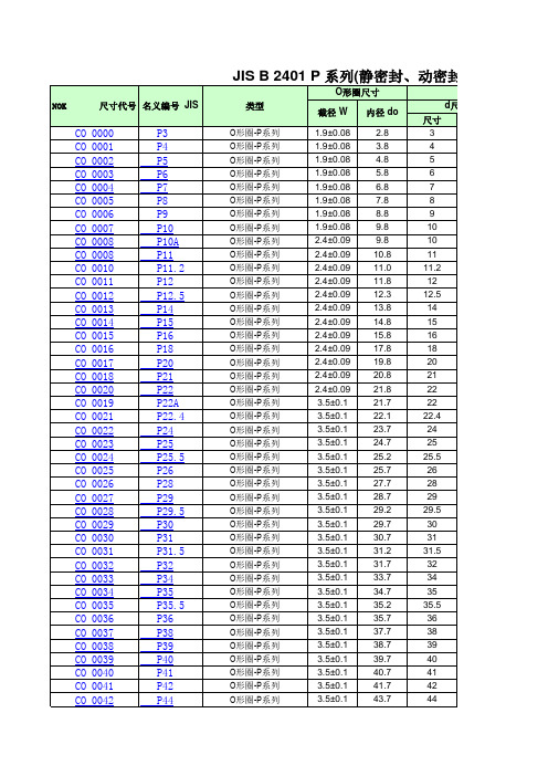
44.7 45.7 47.7 48.7 49.7 47.6 49.6 51.6 52.6 54.6 55.6 57.6 59.6 61.6 62.6 64.6 66.6 69.6 70.6 74.6 79.6 84.6 89.6 94.6 99.6 101.6 104.6 109.6 111.6 114.6 119.6 124.6 129.6 131.6 134.6 139.6 144.6 149.6 149.5 154.5 159.5 164.5 169.5 174.5 179.5 184.5 189.5
3.5± 0.1 3.5± 0.1 3.5± 0.1 3.5± 0.1 3.5± 0.1 5.7± 0.13 5.7± 0.13 5.7± 0.13 5.7± 0.13 5.7± 0.13 5.7± 0.13 5.7± 0.13 5.7± 0.13 5.7± 0.13 5.7± 0.13 5.7± 0.13 5.7± 0.13 5.7± 0.13 5.7± 0.13 5.7± 0.13 5.7± 0.13 5.7± 0.13 5.7± 0.13 5.7± 0.13 5.7± 0.13 5.7± 0.13 5.7± 0.13 5.7± 0.13 5.7± 0.13 5.7± 0.13 5.7± 0.13 5.7± 0.13 5.7± 0.13 5.7± 0.13 5.7± 0.13 5.7± 0.13 5.7± 0.13 5.7± 0.13 8.4± 0.15 8.4± 0.15 8.4± 0.15 8.4± 0.15 8.4± 0.15 8.4± 0.15 8.4± 0.15 8.4± 0.15 8.4± 0.15
P195 P200 P205 P209 P210 P215 P220 P225 P230 P235 P240 P245 P250 P255 P260 P265 P270 P275 P280 P285 P290 P295 P300 P305 P310 P315 P320 P325 P330 P335 P340 P345 P350 P355 P360 P365 P370 P375 P380 P385 P390 P395 P400 P405 P410 P415 P420
PMBT3904,215;PMBT3904,235;中文规格书,Datasheet资料

Product data sheet Supersedes data of 1999 Apr 272004 Jan 12NPN switching transistor PMBT3904FEATURES•Collector current capability I C = 200 mA •Collector-emitter voltage V CEO = 40 V.APPLICATIONS•General switching and amplification.DESCRIPTIONNPN switching transistor in a SOT23 plastic package. PNP complement: PMBT3906.MARKINGNote1.* = p : Made in Hong Kong.* = t : Made in Malaysia.* = W : Made in China.QUICK REFERENCE DATA PINNINGTYPE NUMBER MARKING CODE(1) PMBT3904*1ASYMBOL PARAMETER MAX.UNIT V CEO collector-emitter voltage40VI C collector current (DC)200mAPIN DESCRIPTION1base2emitter3collectorORDERING INFORMATIONTYPE NUMBERPACKAGENAME DESCRIPTION VERSIONPMBT3904−plastic surface mounted package; 3 leads SOT23NPN switching transistorPMBT3904LIMITING VALUESIn accordance with the Absolute Maximum Rating System (IEC 60134).Note1.Transistor mounted on an FR4 printed-circuit board.THERMAL CHARACTERISTICS Note1.Transistor mounted on an FR4 printed-circuit board.CHARACTERISTICST amb = 25 °C unless otherwise specified.SYMBOL PARAMETERCONDITIONS MIN.MAX.UNITV CBO collector-base voltage open emitter −60V V CEO collector-emitter voltage open base −40V V EBO emitter-base voltage open collector−6VI C collector current (DC)−200mA I CM peak collector current −200mA I BM peak base current −100mA P tot total power dissipation T amb ≤ 25 °C; note 1−250mW T stg storage temperature −65+150°C T j junction temperature−150°C T amb operating ambient temperature−65+150°CSYMBOL PARAMETERCONDITIONS VALUE UNIT R th(j-a)thermal resistance from junction to ambientnote 1500K/WSYMBOL PARAMETERCONDITIONSMIN.MAX.UNIT I CBO collector cut-off current I E = 0; V CB = 30 V −50nA I EBO emitter cut-off current I C = 0; V EB = 6 V−50nAh FEDC current gainV CE = 1 V; see Fig.2; note 1I C = 0.1 mA 60−I C = 1 mA 80−I C = 10 mA 100300I C = 50 mA 60−I C = 100 mA30−V CEsat collector-emitter saturation voltageI C = 10 mA; I B = 1 mA −200mV I C = 50 mA; I B = 5 mA −300mV V BEsat base-emitter saturation voltage I C = 10 mA; I B = 1 mA 650850mV I C = 50 mA; I B = 5 mA−950mV C c collector capacitance I E = I e = 0; V CB = 5 V; f = 1 MHz −4pF C eemitter capacitanceI C = I c = 0; V BE = 500 mV; f = 1 MHz−8pFNPN switching transistor PMBT3904Note1.Pulse test: t p ≤ 300 µs; δ ≤ 0.02.f T transition frequency I C = 10 mA; V CE = 20 V; f = 100 MHz300−MHz Fnoise figureI C = 100 µA; V CE = 5 V; R S = 1 k Ω; f = 10 Hz to 15.7 kHz −5dBSwitching times (between 10% and 90% levels); see Fig.3t d delay time I Con = 10 mA; I Bon = 1 mA; I Boff = −1 mA−35ns t r rise time −35ns t s storage time −200ns t f fall time−50nsSYMBOL PARAMETERCONDITIONSMIN.MAX.UNITNPN switching transistor PMBT3904NPN switching transistor PMBT3904NPN switching transistor PMBT3904 PACKAGE OUTLINENPN switching transistorPMBT3904DATA SHEET STATUSNotes1.Please consult the most recently issued document before initiating or completing a design.2.The product status of device(s) described in this document may have changed since this document was publishedand may differ in case of multiple devices. The latest product status information is available on the Internet at URL . DOCUMENT STATUS (1)PRODUCT STATUS (2)DEFINITIONObjective data sheet Development This document contains data from the objective specification for product development.Preliminary data sheet Qualification This document contains data from the preliminary specification. Product data sheet ProductionThis document contains the product specification.DISCLAIMERSGeneral ⎯ Information in this document is believed to be accurate and reliable. However, NXP Semiconductors does not give any representations or warranties,expressed or implied, as to the accuracy or completeness of such information and shall have no liability for the consequences of use of such information.Right to make changes ⎯ NXP Semiconductors reserves the right to make changes to informationpublished in this document, including without limitation specifications and product descriptions, at any time and without notice. This document supersedes and replaces all information supplied prior to the publication hereof.Suitability for use ⎯ NXP Semiconductors products are not designed, authorized or warranted to be suitable for use in medical, military, aircraft, space or life support equipment, nor in applications where failure or malfunction of an NXP Semiconductors product can reasonably be expected to result in personal injury, death or severe property or environmental damage. NXP Semiconductors accepts no liability for inclusion and/or use of NXP Semiconductors products in such equipment orapplications and therefore such inclusion and/or use is at the customer’s own risk.Applications ⎯ Applications that are described herein for any of these products are for illustrative purposes only. NXP Semiconductors makes no representation or warranty that such applications will be suitable for the specified use without further testing or modification.Limiting values ⎯ Stress above one or more limiting values (as defined in the Absolute Maximum Ratings System of IEC 60134) may cause permanent damage to the device. Limiting values are stress ratings only and operation of the device at these or any other conditions above those given in the Characteristics sections of this document is not implied. Exposure to limiting values for extended periods may affect device reliability.Terms and conditions of sale ⎯ NXP Semiconductors products are sold subject to the general terms and conditions of commercial sale, as published at /profile/terms, including those pertaining to warranty, intellectual property rightsinfringement and limitation of liability, unless explicitly otherwise agreed to in writing by NXP Semiconductors. In case of any inconsistency or conflict between information in this document and such terms and conditions, the latter will prevail.No offer to sell or license ⎯ Nothing in this document may be interpreted or construed as an offer to sell products that is open for acceptance or the grant, conveyance or implication of any license under any copyrights, patents or other industrial or intellectual property rights.Export control ⎯ This document as well as the item(s) described herein may be subject to export controlregulations. Export might require a prior authorization from national authorities.Quick reference data ⎯ The Quick reference data is an extract of the product data given in the Limiting values and Characteristics sections of this document, and as such is not complete, exhaustive or legally binding.NXP SemiconductorsCustomer notificationThis data sheet was changed to reflect the new company name NXP Semiconductors. No changes were made to the content, except for the legal definitions and disclaimers.Contact informationFor additional information please visit: For sales offices addresses send e-mail to: salesaddresses@© NXP B.V. 2009All rights are reserved. Reproduction in whole or in part is prohibited without the prior written consent of the copyright owner.The information presented in this document does not form part of any quotation or contract, is believed to be accurate and reliable and may be changed without notice. No liability will be accepted by the publisher for any consequence of its use. Publication thereof does not convey nor imply any license under patent- or other industrial or intellectual property rights.Printed in The Netherlands R75/04/pp9 Date of release: 2004 Jan 12Document order number: 9397 750 12461分销商库存信息:NXPPMBT3904,215PMBT3904,235。
- 1、下载文档前请自行甄别文档内容的完整性,平台不提供额外的编辑、内容补充、找答案等附加服务。
- 2、"仅部分预览"的文档,不可在线预览部分如存在完整性等问题,可反馈申请退款(可完整预览的文档不适用该条件!)。
- 3、如文档侵犯您的权益,请联系客服反馈,我们会尽快为您处理(人工客服工作时间:9:00-18:30)。
Applicationsq Digital mobile cellular systems as GSM, DAMPS, JDCq Various demodulation schemes, such as PM, PSK, FSK, QAM, QPSK, GMSK q Space and power saving optimizations of existing discrete demodulator circuitsFunctional DescriptionThe PMB 2402 is a single-chip single-conversion heterodyn PM-receiver with phase shifting circuitry for the I/Q-phase baseband demodulation on chip. It also includes the second local oscillator, a gain controlled second IF-amplifier, two differential operational amplifiers for baseband filtering purposes and power down circuitry.The PMB 2402 is designed for digital mobile telephones according to the GSM-standard and other digital systems.Type Version Ordering Code Package PMB 2402S V 2.1Q67000-A6072P-DSO-28-4(Shrink, SMD))PMB 2402SV 2.1Q67006-A6072P-DSO-28-4 (Shrink,SMD, Tape + Reel)GSM Receiver Circuit Preliminary Data Bipolar ICPMB 2402FeaturesqHeterodyne receiver with demodulatorq Down mixing from 900 MHz receiver band to the base bandq Demodulation and generation of I/Q-baseband componentsq Low mixer noise 10 dB (SSB)q Input high intercept point + 2 dB q Integrated 0˚ and 90˚ phase shifter q 82 dB AGC-rangeq On-chip second LO-oscillator with external tuning circuit q Two differential operational amplifiersq Low power consumption due to highly flexible power-down capabilityq Wide input frequency range up to 1 GHz q Wide IF-range from 35 MHz to 100 MHzq Wide output frequency range up to 13.5 MHz q P-DSO-28-4 shrink packageqTemperature range – 25˚C to 85˚CP-DSO-28-4Pin Configuration (top view)Pin Definitions and FunctionsPin No.Symbol Function1SOI Non-inverting in-phase signal output2SOQ Non-inverting quadratur signal output3INQ Inverting op. amp. signal output (Q)4OUTQ Non-inverting op. amp. signal output (Q) 5OUTQ Inverting op. amp. signal output (Q)6INQ Non-inverting op. amp. signal intput (Q) 7SOQ Inverting quadratur signal output8LO2E External capacitors for oscillator9LO2B VCO-tuning circuit10GND Ground11IFI Inverting IF input12IFI Non-inverting IF input13GC Gain control input14LO2O VCO-signal output15MO Inverted output of first mixer16MO Non-inverted output of first mixer17V S Supply voltage18SI Non-inverted signal input of first mixer19SI Inverted signal input of first mixer20PD1Power-down input 121LO1Non-inverting input for first local oscillator 22LO1Inverting input for first local oscillator23PD2Power-down input 224SOI Inverting in-phase signal output25INI Non-inverting op. amp. signal input (I)26OUTI Inverting op. amp. signal output (I)27OUTI Non-inverting op. amp. signal output (I) 28INI Inverting op. amp. signal input (I)Block DiagramCircuit DescriptionThe input signal SI/SI and the amplified first local oscillator signal LO1/LO1 are mixed down to an intermediate frequency (IF). The open collector output of the mixer generates a differential current at pins MO/MO which is filtered by an external resonant circuit. The resulting voltage drives an external SAW-filter.The second local oscillator signal LO2 is generated in an on chip VCO and is fed to two dividers, which generate orthogonal signals at a quarter of VCO-frequency. The internal LO-signal is fed to an additionally divider, whose output signal LO2O is fed to the RF-signal of PLL-synthesizer. The filtered IF-signal reenters the chip at the IFI/IFI input, where it is amplified and demodulated to the final baseband output frequency with each of the orthogonal signals. The resulting in-phase and quadrature signals pass through differential output drivers and appear at SOI/SOI and SOQ/SOQ outputs, respectively. The amplification of the IF-signal before the second mixer stage is performed by a gain-controlled amplifier, the gain being determined by the voltage at the gain control input GC. Two differential operational amplifiers with the input signals INI/INI (INQ/INQ) and the output signals OUTI/OUTI (OUTQ/OUTQ) can be used as active filters.Differential signals and symmetrical circuitry are used throughout, except at the signal output. Bias drivers generate internal temperature- and supply voltage-compensated reference voltages required by various circuit blocks. Switching the power down inputs PD1 and PD2 from high to low (see table) sets the circuit from its normal operating mode into a mode with reduced supply current. PD1PD2RF-Part IF-Part VCO/DivdersL L OFF OFF ONL H OFF ON ONH L ON OFF ONH H ON ON ONInternal Input / Output CircuitsElectrical CharacteristicsAbsolute Maximum RatingsThe maximum ratings may noy be exceeded under any circumstances, not even momentarily and individually, as permanent damage to the IC will result.TA= –25˚C to 85˚CParameter Symbol Limit Values Unit Remarksmin.max.Supply voltage V S– 0.57VInput/output voltage(any except open collector)VIO– 0.5– 0.5VS+ 0.57.5VVVS≤ 7 VVS≤ 7 VOpen collector output voltage (MO/MO)VOC– 0.5– 0.5VS+ 2.57.5VVVS≥ 5 VVS≥ 5 VDifferential input voltage (any differential input)VI– 33VJunction temperature T j125˚C Storage temperature T stg– 55125˚CThermal resistence (junction to ambient)Rth JA55K/WK/WPDSO-28P-DSO-28-SOperational RangeWithin the operational range the IC operates as described in the circuit description. The AC/DC-characteristics limits are not guaranteed.V S = 4.5V to 5.5V; T A = –25˚C to 85˚C; refer to test circuit 1.Note:Power levels are referred to resistance of 50ΩParameter SymbolLimit Values UnitRemarksmin.max.SI/SI input level P SI – 11dBm SI/SI input frequency f SI 1000MHz LO1/LO1 input level P LO1– 113dBm LO1/LO1 input frequency f LO11100MHz Intermediate frequency f IF 35100MHz IFI/IFI input level P IFI – 24dBm IFI/IFI input frequency f IFI 35100MHz LO2 input level P LO2– 200dBm VCO externalLO2 input frequency f LO2140400MHz VCO frequency range f VCO 120250MHz with ext. capacitors LO2O output level P LO2O 120180mVpp LO2O output frequency f LO2O 1550MHz SOI/SOI, SOQ/SOQ output Bandwidth B SO 013.5MHz – 3 dB roll off GC input voltage V GC 02V L-PD1/PD2 voltage V PDL 01V H-PD1/PD2 voltageV PDH4V SVAC/DC CharacteristicsAC/DC-characteristics involve the spread of values guaranteed within the specified supply voltage and ambient temperature range. Typical characteristics are the median of the production.VS= 4.75 to 5.25V; T A = 25˚C;Parameter Symbol Limit Values Unit Test Condition TestCircuitmin.typ.max.Supply current I S 3.11211.5205.515.51524.56.81918.530mAmAmAmAPD1 = L PD2 = LPD1 = L PD2 = HPD1 = H PD2 = LPD1 = H PD2 = L1First Mixer Signal Input SI/SIInput resistance R SI172533Ω2a Input inductance L SI 3.55 6.5nH In series to R SI2a Max. input level P SI– 13– 11dBm 1 dB compr. at MO/MO1Input intercept Point PIPI023dBm G MO = 14 dB1Blocking level P B– 16– 14– 12dBm 3 dB attenuation ofwanted Signal at MO1Input interference level at f =f int Pint– 38dBm– 98 dBm interference atf = (fint+/–f LO1) X2 at MO3Input frequency f SI960MHz1Noise figure N SINSI 7.59.58109.511.5dBdBDSB-noise,f C = 900 MHzSSB-noise,f C = 900 MHzincluding optimum noisematching1Output of First Mixer MO/MO (open collector)Output resistance R MORMO 11.27161020.813kΩkΩfMO= 45 MHzfMO= 71 MHz2c2cOutput capacitance C MO0.71 1.3pF parallel to R MO2c Total output current I MO +MO 3.55 6.5mA1Power gain from Signal input GMO1314dB1Intermediate frequency fIF35100MHz1AC/DC-Characteristics (cont’d)ParameterSymbolLimit Values UnitTest ConditionTest Circuitmin.typ.max.Input of First Mixer Local Oscillator LO1/LO1Input resistance R LO1490700910Ωf LO1 = 900 MHz2a Input capacitance C LO10.711.3pF parallel to R LO12a Input level P LO1V LO1– 111783890dBm mVppsee diagram 111Input frequencyf LO11100MHz1Isolation of First Mixer From SIto MO A SI – MO 30dB f SI = 945 MHz;f LO1 = 900 MHz 1SIto LO1A SI – LO160dB f SI = 945 MHz;f LO1 = 900 MHz 1LO1to MO A LO1 – MO 50dB f SI = 945 MHz;f LO1 = 900 MHz 1LO1to SI A LO1 – SI 60dB f SI = 945 MHz;f LO1 = 900 MHz 1MO to Si A MO – SI50dB f SI = 945 MHz;f LO1 = 900 MHz 1MO to LO1A MO – LO165dBf SI = 945 MHz;f LO1 = 900 MHz1IF Input IFI/IFI Input resistance R IFI 6390117Ω2a Input capacitance C IFI 0.350.50.65pF parallel to R IFI2a Max. input level P IFI V IFI – 1789dBm mVppV GC = 2 V, 1 dB compr. atSO;see diagram 411Input intercept pointP IPI see diagram 51Input frequency f SI 35100MHz 1Noise figureN SI101114dBSSB-noise1Input for Second Local Oscillator LO2 (VCO external)Input resistanceR LO21.91.32.41.83.12.3k Ωk Ωf LO2 = 180 MHz f LO2 = 360 MHz2b 2bAC/DC-Characteristics(cont’d)Parameter Symbol Limit Values Unit Test Condition TestCircuitmin.typ.max.Input capacitance C LO20.71 1.3pF2bInput level P LO2VLO2– 2063630dBmmVppinto 50Ω 1.11.1Input frequency f LO2140400MHz 1.1 Voltage Controlled Oscillator VCO (LO2)VCO-frequency f VCO120250MHz with ext. capacitors 1.2 VCO Output LO2OOutput resistance R LO2O0.9 1.2 1.5kΩOutput capacitance C LO2O0.71 1.3pFOutput level V LO2O150120160140mVppmVppIF≤ 75 MHzIF≥ 75 MHz11Output frequency f LO2O1550MHz1 Signal Outputs SOI/SOI, SOQ/SOQOutput resistance R SO175250325ΩOutput capacitance C SO0.71 1.3pFSO frequency roll off fSO13.5MHz see diagram 6DC output level V SO 2.0 2.5V1Diff. output offset voltage VSO/SO28mV between I/I or Q/Q1Voltage gain from IF to I/Q-output GSO57– 2561– 2165– 17dBdBVGC= 0 V see dia-VGC= 2 V gram 2 + 31Gain Control Input GCGC-input voltage V GC02V1 GC-input current–I GC1µA0V≤V GC≤ 2 V1 Gain control factor F GC40dB/V F GC = d G SO/d V GCsee diagram 31AC/DC-Characteristics(cont’d)Parameter Symbol Limit Values Unit Test Condition TestCircuitmin.typ.max.Power-Down Inputs PD1, PD2L-PD input voltage V PDL01V1L-PD input current I PD1LIPD2L 0.10.2µAµA0≤V PD1, 2L≤ 1 V1H-PD input voltage V PDH4V S V1 H-PD input current I PDH10µA4≤V PD1, 2L≤V S1Differential Operational Amplifier (open loop)Slew rate SR 4.6V/µs1 Gain BandwithProd.GBW12MHz1 Voltage gain A Vo55dB1 Phase marginϕR60degr.1 Gain margin A R14dB1 Common modeRejection RatioCMRR58dB1 Offset voltage V OFF1mV1 Output voltage V OUT0.8V S–1V1Test Circuit 1Test Circuit 1.1Test Circuit 1.2Test Circuit 2aTest Circuit 2bTest Circuit 2cThe S-parameters are tested at the indicated frequency and the equivalent parallel or series circuit is calculated on this base.Test Point Test Circuit Test Frequency / MHz Pin x Pin yLO1-input impedance2a9002122SI-input impedance2a9001819IFI-input impedance2a45 (901112)LO2-input impedance2b180, 3609–MO-output impedance2c45, 711516Test Circuit 3f W = wanted input signal from received channelf int = unwanted interfering signal within band :f int =f LO –f IF / 2f LO = local oscillator signalf IFW = wanted IF signal from received channel =f LO –f Wf IFi t = unwanted IF / 2 signal from interfering channel:f IFint =f LO –f intfIF2in= unwanted harmonic signal of f IF2in :f IF2in = 2×f IFintApplication CircuitDiagram 1First Mixer Gain versus LO-Level P LO1P SI = – 40 dBm,f MO = 45 MHz Diagram 3Gain Control Characteristic Voltage Gain G SO versus GC-Voltage VGCDiagram 2Gain Control Characteristic Output LevelP SO versus input Level P IFIDiagram 4Gain Control CharacteristicMax. Input Level P IFI versus GC-Voltage V GC :(1 dB Compresion at SO)Diagram 5Gain–Control Characteristic Input Intercept Point P IPI versus GC-Voltage VGCDiagram 6Frequency Transfer Characteristic ofOutputs SOI / SOQSemiconductor Group21Package Outlines Plastic-Package, P-DSO-28-4 (Shrink) (SMD)(Dual-Small-Outlines) PMB 2402Dimensions in mm Sorts of Packing Package outlines for tubes, trays ect. are contained in our Data Book “Package Information”SMD = Surface Mounted Device元器件交易网。